1
Introduction to Virtuoso Electrically Aware Design Flow
The reducing sizes of advanced integrated circuits means that wire widths are becoming smaller and the lengths of connecting wires longer. In addition, there is an exponential increase in the density of the current flowing through the wires. As a result, integrated circuits become more vulnerable to electromigration (EM), which is the gradual dislocation of metal atoms in a conductor.
To produce a reliable and sustainable integrated circuit, it is therefore essential that you perform comprehensive electromigration checks and ensure that the physical design of every design component is electrically correct by construction and optimized to meet the design intent.
The Virtuoso Electrically Aware Design (EAD) flow lets you capture the current data from design simulations, extract and visualize RC parasitics as you edit the layout, perform EM checks and fix violations. You can further extract parasitics from a partial or a complete layout and rerun simulations to check if the output specifications are met. This flow guide describes the Virtuoso EAD flow in detail and explains how to use the various tools to perform EM analysis for your design.
This chapter describes the following:
Licensing Requirements
The EAD flow uses the following licenses:
What is Electromigration?
Electromigration (EM) is the term used to describe the movement of atoms in a solid conductor resulting from collisions between the flow of electrons and metal atoms in connecting wires.
This movement of atoms is caused by high current stress in metal wires generated by the movement of electrons. As the electrons move through a metal wire, they collide with the atoms in the wire, causing the wires to become heated. If enough electrons collide with a metal atom over a period of time, the metal atom can move in the direction of the electron flow, potentially causing
- An open circuit if enough atoms move and cause the wire to break
- A short to an adjacent metal wire if enough atoms move to the same location
EM can damage the interconnect wires and vias, thereby causing degradation in the performance of an integrated circuit. Therefore, it is important to observe the electrical impact of the physical design of every component.
The EAD flow in Virtuoso involves various steps to perform comprehensive EM checks for your design and make it electrically correct. The following section provides a brief description of this flow.
A Snapshot of The Electrically Aware Design Flow
The following diagram provides a snapshot of the EAD flow.
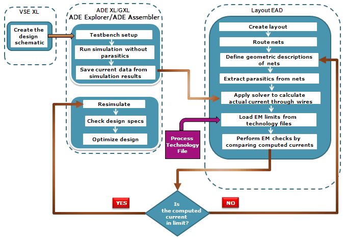
You begin by creating a schematic, running simulations, and modifying your design so that it meets the desired specifications. When the specifications are met, you then configure the testbench to
EM depends on various factors, such as the local current density (current per unit area), the homogeneity of the current flow through a region, and the EM length. All these factors are captured for different conductor layers and vias as rules in technology files for each process technology specification.
Before performing the EM checking, launch the EAD Browser in either Layout EXL or Layout MXL. Next,
As you create or modify the layout of your design, an extraction engine in Layout EAD lets you
You can now
You can then
At any point in the flow, you can take the parasitics from your partially complete or completed layout and
The following chapters in this flow guide describe the Virtuoso EAD flow in detail and explain how to use the various Virtuoso tools to perform EM analysis and parasitic resimulation for your design.
Related Videos
Related Blog
Return to top