4
Extracting Parasitics in the Layout View
This chapter explains how you extract and analyze parasitic information from a partial or complete layout view using the EAD Browser for a layout view. EAD Browser is an assistant you use to drive your electrically-aware design session.
One of the main benefits of the EAD Browser is that it can be used to analyze parasitic information for both partially and fully completed layouts. Not all devices and nets need to be routed before you launch EAD Browser, and you can place and route devices while the application is running.
This section explains how to start EAD Browser from a schematic or layout view, and provides details on the EAD workspace and EAD Browser. It goes on to explain how to define and manage EAD setup and process information and then use that setup to extract parasitics for your design and analyze the results in the EAD Browser and layout canvas.
- Starting EAD Browser for a Layout
- The EAD Workspace
- Managing EAD Setups
-
Extracting and Analyzing Parasitics
Starting EAD Browser for a Layout
Starting EAD from a Layout Window
You can also start EAD from a layout window. To do this,
-
From the menu bar, Launch – Layout EAD.
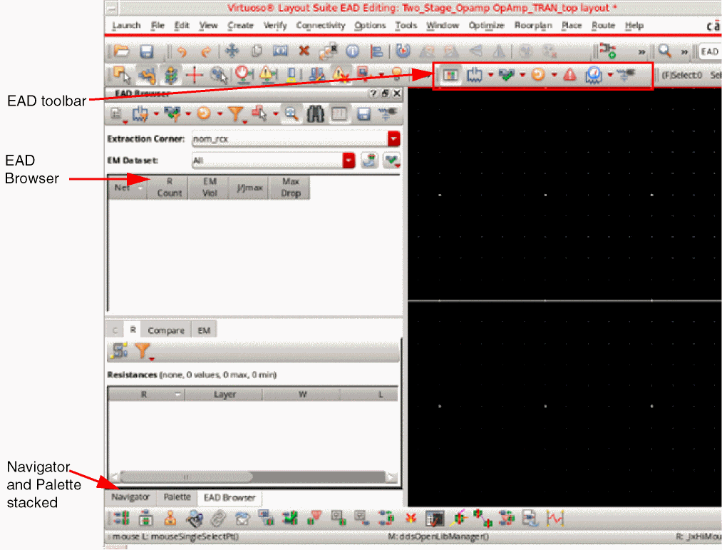
Virtuoso Layout Suite EAD is launched and The EAD Workspace is loaded. This workspace opens the EAD Browser assistant on the left of the layout canvas.
Starting EAD Browser
You start Layout EXL or Layout MXL in the same way as Layout XL; either from a schematic view that is open in the Virtuoso Schematic Editor or from a layout view that is open in Virtuoso Layout Suite.
EAD and its various features are enabled only while you are in the Layout EXL or in Layout MXL application. When you close Layout EXL or switch to another VLS tier, all EAD-specific data and features are removed from the layout window.
Starting Layout EAD from a Schematic View
To start Layout EAD from a schematic view,
- From the schematic editor menu bar, choose Launch – Layout EXL, or Launch – Layout MXL.
-
The Startup Option form is displayed.
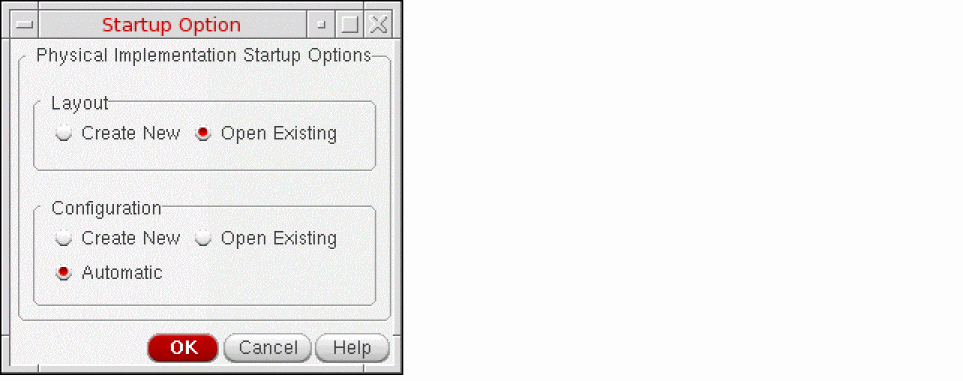
- In the Layout group box, choose whether you want to create a new layout cellview or open an existing one.
-
In the Configuration group box, choose Automatic and then click OK.
One of the following happens.-
If you chose to create a new layout view, the New File form is displayed.
Click OK to create the new layout cellview. -
If you chose to open an existing layout view, the Open File form is displayed.
Specify the Library and Cell names and choose the View you want to open from the cyclic field.Click OK to open the cellview.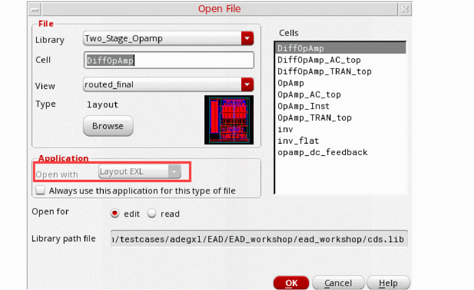
-
If you chose to create a new layout view, the New File form is displayed.
-
In Layout EXL, choose EAD from the Workspace Configuration drop-down list.
The EAD workspace displays the EAD Toolbar and three stacked assistants: the EAD Browser, the Navigator, and the Palette.
Starting EAD from a Layout Window
You can also start EAD from a layout window. To do this,
-
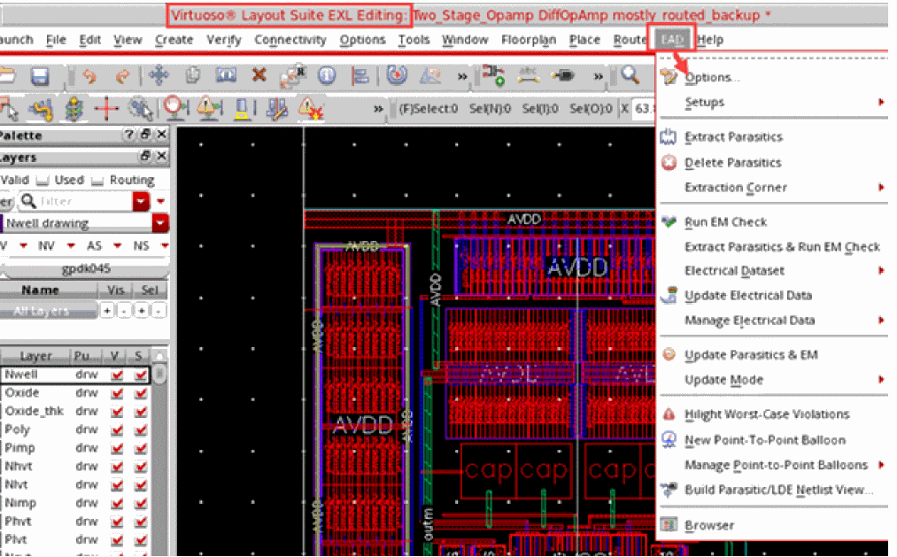
From the menu bar, Launch – Layout EXL.
Virtuoso Layout Suite EXL is launched. The EAD menu is also added the menu bar, as shown below.
-
Choose EAD – Browser.
The EAD Browser is displayed on the left of the layout canvas, as shown below.
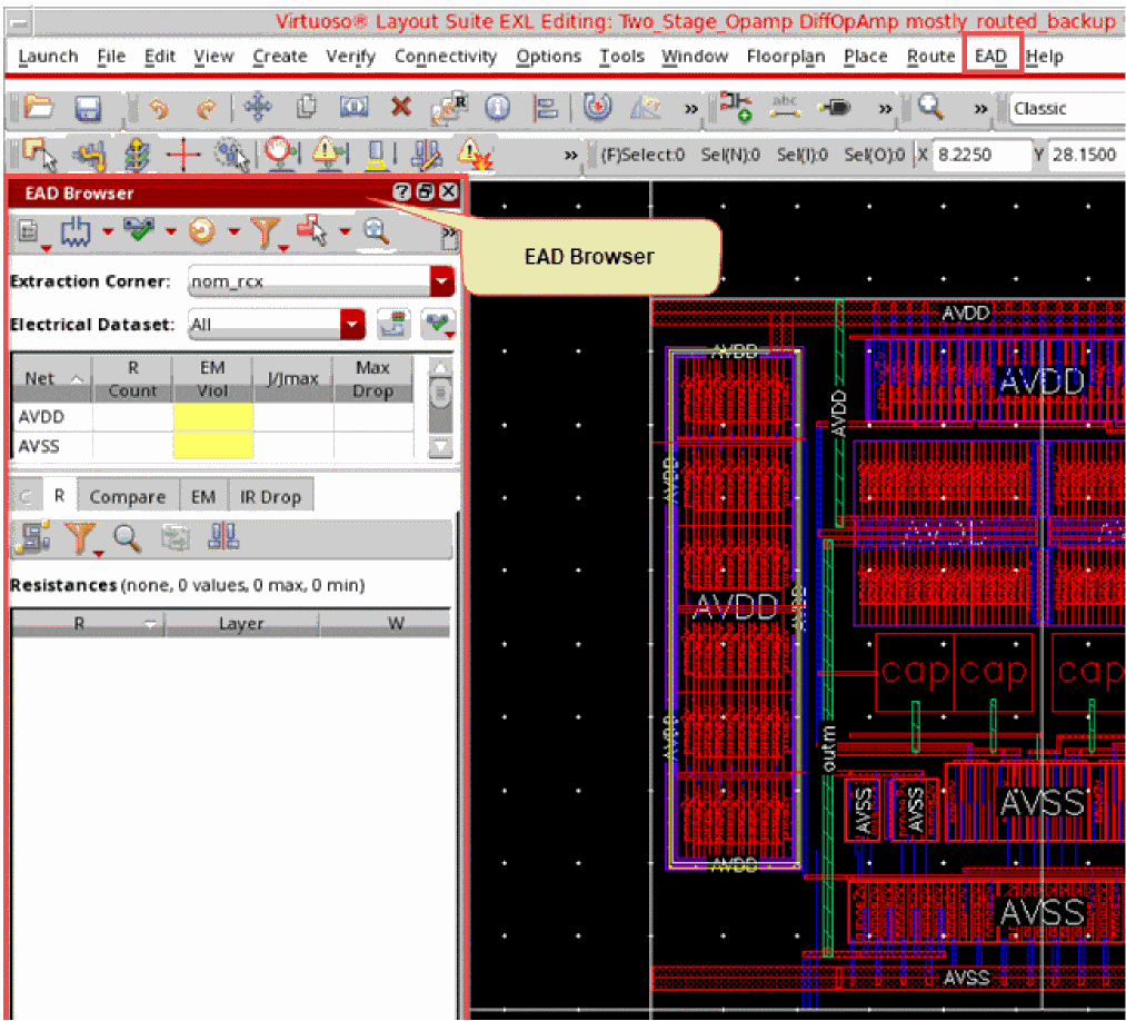 The EAD workspace displays the EAD Toolbar and three stacked assistants: the EAD Browser, the Navigator, and the Palette.
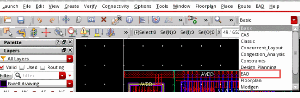
The EAD Workspace
The EAD workspace is designed to help you drive parasitic extraction and EM analysis, and is installed automatically when you launch Layout EAD from the layout or schematic view.
The workspace comprises the following elements:
- EAD Toolbar, which lets you access high level Layout EAD functions with a single mouse click. For more information, see EAD Toolbar.
- EAD Browser assistant, which you use to drive parasitic extraction and EM analysis for your design. For more information, see EAD Browser.
-
Navigator assistant, which shows a hierarchical representation of all the devices, nets, and pins in the design. When the layout of the top level is in view, if you select a hierarchical net in the Navigator assistant, the corresponding net is highlighted in the EAD Browser. When multiple nets are selected, EAD uses a different color for each net.
For more information, see Navigator. - Palette assistant, which lets you define how layers, objects, and guides are displayed in the layout window. For more information, see Palette Panels in the Virtuoso Layout Suite L User Guide.
EAD Toolbar
The EAD toolbar lets you access the main EAD functions with a single mouse click.
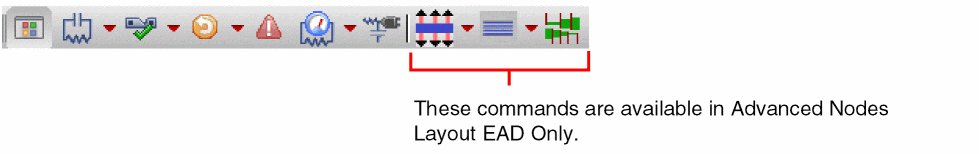
For more information on the individual buttons on the toolbar, see the table below.
| Icon | Commands | Lets you... |
|---|---|---|
|
Toggle the display of the EAD Browser assistant in the layout window. |
||
|
Extract and delete parasitics for the current design. See Extracting and Analyzing Parasitics for more information.
You can also delete parasitic information programmatically using the elecUpdateDataSetParamsPropValue SKILL function.
To delete parasitics for selected nets only, select one or more nets in the Summary Pane, right-click and choose Delete Parasitics. |
||
|
Run electromigration checks for all the nets in the current design. You can optionally extract parasitics and update electrical data before the EM check is run; and update the electrical data for the design. |
||
|
Delete the electrical data already extracted and displayed in the EAD Browser. |
||
|
Write electrical data information for the existing datasets to the terminals or instance terminals for which the current data is missing or out of sync because they are newly created, modified, or recreated due to layout edits. |
||
|
Update the parasitic and electromigration data for the current design.
When you run these commands, any net that has been extracted previously is updated even if the parasitics have been deleted due to some other action. See Extracting Parasitics in Layout EAD for more information. |
||
|
Highlight the worst-case EM violations in the layout window. While using this feature, dim the design in the canvas using the Dim command on the Options toolbar of VLS XL. This enhances the view of the main electromigration issues in your design. |
||
|
Select two points on a net to see electrical information between those two points. See Using Point-To-Point Info Balloons for more information. |
||
|
Open the |
||
|
Run EM trunk optimization commands. The three commands are Expand to Fix EM Violations, Shrink Oversized Trunks, and Shrink and Expand. |
||
|
Select the style for optimizing a trunk to resolve EM violations. The three styles are Widen - No Stranding, Parallel Stranding, and Stacked Stranding. |
||
|
Enable trunk tapering during trunk widening. Trunk tapering only works for the Widen style and not for parallel or stacked stranding. |


EAD Browser
You use the EAD Browser to obtain visual feedback on the parasitics and electromigration issues in your design and to view the effects of any changes you make in order to solve these issues. It provides information about your design beyond that available in either the Annotation Browser and Navigator assistants and supports all the relevant Layout XL commands.
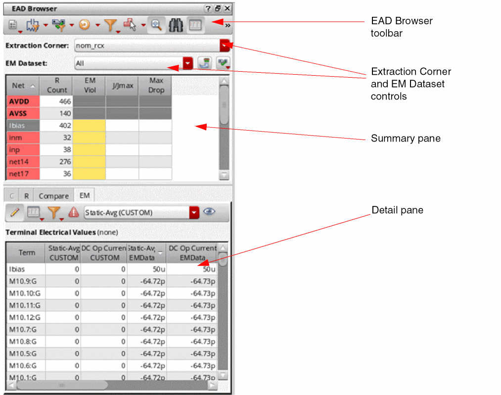
The browser has four main components:
EAD Browser Toolbar
The EAD Browser toolbar lets you access the main Layout EAD functions with a single mouse click (three of the buttons are also present on the main EAD Toolbar.)
The buttons are organized from left to right to reflect the basic Layout EAD flow. For more information on the functions available, see the table below.
| Icon | Commands | Lets you... |
|---|---|---|
|
Choose a predefined setup to use for the current session or open the EAD Options form to change any settings or create a new setup if required. See Managing EAD Setups for more information. |
||
|
Extract Parasitics for Filtered Nets
Delete Parasitics for Filtered Nets |
Extract and delete parasitics only for the filtered nets displayed in the EAD Browser. Extract and delete parasitics for all the nets in the current design. The commands to extract or delete parasitics for filtered nets are grayed when no filters are applied. See Extracting and Analyzing Parasitics for more information.
You can also delete parasitic information using the elecUpdateDataSetParamsPropValue SKILL function.
|
|
|
Run electromigration checks only for the filtered nets displayed in the EAD Browser. Run electromigration checks for all the nets in the current design. The Run EM Check On Filtered Nets command is grayed when no filters are applied. |
||
|
You can optionally extract parasitics and update electrical data before the EM check is run; and update the electrical data for the design. |
||
|
Transfers the electrical datasets from ADE Assembler, or schematic to the layout. While doing this, if EAD finds that the name of the dataset being transferred matches with the name of an existing dataset at the layout side, it compares the timestamps of the two. If their timestamp is same, no action is taken. If their timestamp is different, the tool shows a dialog box and prompts you to confirm whether the dataset at the layout side should be overwritten. If you confirm, it deletes the existing dataset and copies the newer version to the layout. Before deleting the dataset at the layout side, EAD ensures that the results database is accessible. If, due to some reason, the results database is not accessible, the transfer of that dataset is skipped, and the version already saved with the layout is retained. |
||
|
Deletes the electrical data already extracted and displayed in the EAD Browser. |
||
|
Writes electrical data information for the existing datasets to the terminals or instance terminals for which the current data is missing or out of sync because they are newly created, modified, or recreated due to layout edits. |
||
|
Save custom datasets with a user-defined name. For more details, refer to Creating User-Defined Custom Datasets. |
||
|
Update the parasitic and electromigration data for the current design.
Any net that has previously been extracted is automatically updated in this mode, even if the parasitics have been deleted due to some other user action in the meantime. See Extracting Parasitics in Layout EAD for more information. |
||
|
Filter the data in the browser to show only those nets that meet the selected filter criteria. See Filtering Rows for more information. |
||
|
Specify how selections in the canvas affect the EAD Browser. |
||
|
Automatically pan and zoom to the correct area of the layout view when you select a net or parasitic in the EAD Browser tables. Environment variable: fitToSelected |
||
|
Locate results for a particular net by typing the name of the net into a text box. See Searching Nets for more information. |
||
|
Switch between Single pane view and Dual pane view.
See Toggling Dual Pane and Single Pane View for more information. |
||
|
Export all the data shown in the tables in either HTML or CSV format. |
||
|
Opens the |
||
|
Interactively shows EAD parameters for the segment between any two points on a net. See the Using Point-To-Point Info Balloons section for more information. |
||
|
Opens the EAD - Save State form, which you can use to save the current EAD state. See the Saving an EAD State section for more information. |
||
|
Loads an EAD state that has been saved earlier. See the Loading an EAD State section for more information. |
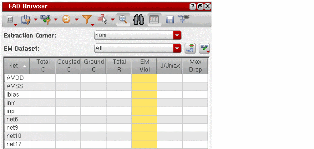
Extraction Corner and EM Dataset Controls
Use these controls to specify which extraction corner results are displayed and which dataset is used to run EM checks and display results.
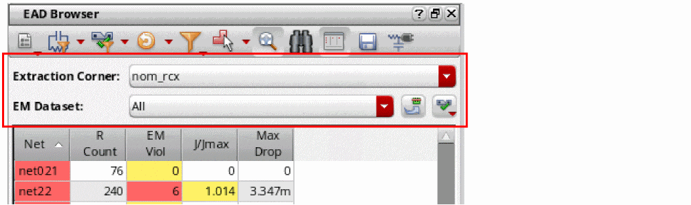
| Form Field | Specifies... |
|---|---|
|
Which extraction corner results are displayed in the EAD Browser.
The default extraction corner is defined in the process settings file (
These corners are defined during EAD Setup in ADE Assembler and mapped to an ICT file, which contains the process information for the corner in question. See Setting up Testbenches and Corners for more information.
|
|
|
Which EM dataset is used to run EM checks and display results. The default is All, which means that EM results are reported for all available datasets.
By default, the datasets are read from the paths saved in the However, if you need to use results from some other dataset, you can use ADE Assembler to overwrite the existing dataset with new simulation data, or load the history results that were used to save the other dataset.
Alternatively, you can use elecUpdateDataSetParamsPropValue to set the paths to another existing dataset. To set these paths, you need the
For example, if the results database and the psf directory to be used are saved in the elecUpdateDataSetParamsPropValue("Two_Stage_Opamp" "DiffOpAmp" "schematic" "emData" "simResDB" "/home/projectA/simulation/vdd13/vdd13.rdb") elecUpdateDataSetParamsPropValue("Two_Stage_Opamp" "DiffOpAmp" "schematic" "emData" "simResDir" "/home/projectA/simulation/vdd13/psf") After setting the paths, click Update Electrical Data on the EAD Browser toolbar to update the electrical data from the specified results database. At any time, you can check the paths to the results database and the psf directory by using elecGetDataSetParamsPropValue. If you specify relative paths in the constraint view or by using elecUpdateDataSetParamsPropValue, Layout EAD resolves them relative to the following directories in the given order of preference: |
|
|
|
That all datasets that have been changed in ADE Assembler are updated in Layout EAD. Use this if you have updated your datasets or created new datasets in ADE Assembler while the layout view is open. |
|
|
Select which EM checks are enabled and disabled.
The EM temperature that you set in the EM tab of the EAD Options form is displayed next to the name of the EM dataset. 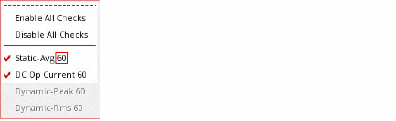 |
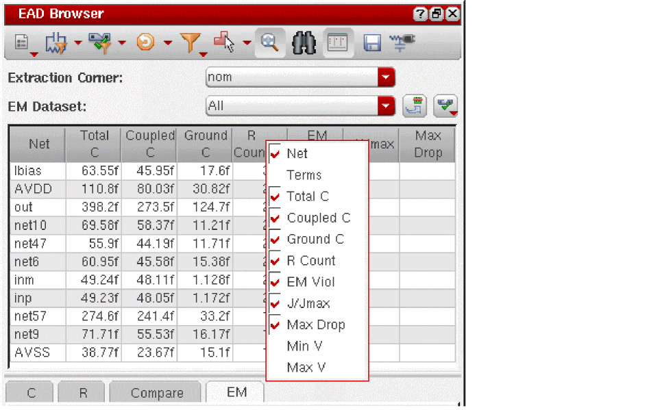
Summary Pane
The summary pane shows a net-specific summary of the parasitic and EM information currently available for each net in the design. The columns displayed depend on the
The following table lists all the columns available in the summary pane:
Some of the columns remain hidden by default. To view any hidden column, right-click in the table header and select the column name from the context menu.
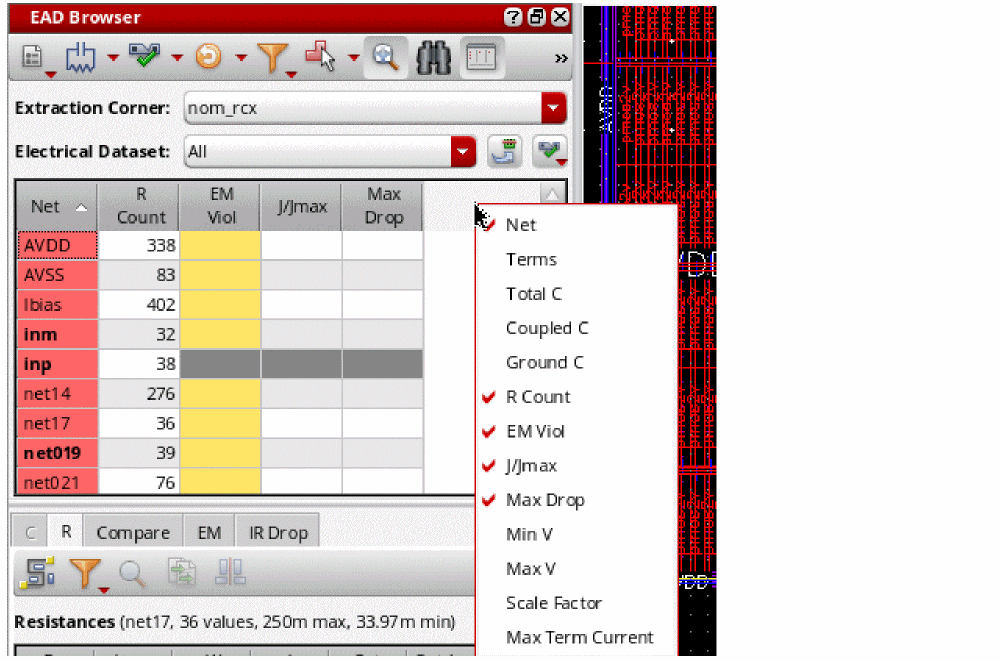
When you first launch Layout EAD, the table lists all the nets in the current design but does not extract parasitics or run any EM checks by default.
After you perform parasitic extraction, the table is updated to show parasitics (total, coupled, and grounded capacitance values and total number of resistors) for the listed nets.
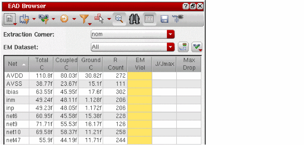
If electrical constraints, such as the Max Capacitance constraint or the Max Resistance constraint, are applied on nets, and the extracted parasitic data violated the constraints, the corresponding cells are highlighted in red. For more details, refer to the Detail Pane.
When you have run an EM check, the summary table updates to show color-coded electromigration information for the listed nets (only some of this information is shown below).
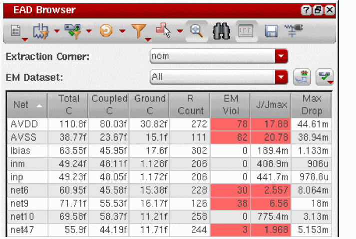
The indication of the different color codes is as given below.
- Red indicates that EM violations were detected
- Yellow indicates that the EM check was skipped for the net
You can find out more about any individual value by clicking one of the table cells to open the EM tab in the Detail Pane.
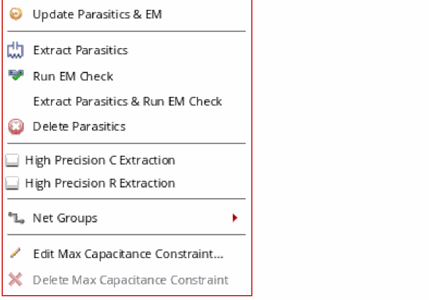
You can right-click in one of the cells to open the context menu, which provides a quick access to commands to update the parasitic and EM data, extract parasitics, and run the EM check for the selected net. For example, to delete parasitics for selected nets only, select one or more nets, right-click and choose Delete Parasitics. The context menu for a net in the summary pane is given below.
Important Points to Note
-
By default, EAD shows the nets in your design from the perspective of the top-level cell of the window. When you edit a cell in place, the list of nets shown in the summary table does not change, unless the cell you are editing in place has been edited and saved in another session since it was loaded into the current session. If nets were added or deleted in that other session, then those changes are reflected when the edit-in-place occurs in the current session.
The display of nets in the summary pane also depends on the setting of the extractNetsWithConstraints environment variable, which controls the display of nets based on the EAD constraints applied to them. If this variable is set tot, only those nets that have EAD constraints applied on them are displayed in the summary table. - By default, the tool performs a fast C and fast R extraction which is based on the models in the technology file, but the extracted data might not meet high accuracy levels. Therefore, to extract capacitance and resistance on critical nets with a higher degree of accuracy, you can selectively enable high precision C and R solvers. This creates a corresponding High Precision C Extraction and High Precision R Extraction constraint based on the options specified on Extraction tab of EAD Options form. It is also recommended to use high precision C extraction when the layout contains non-orthogonal nets. When you turn off high precision extraction, these constraints are deleted.
- The excludePolyDiffusionCap and includePolyFringingCap environment variables can be used to control the inclusion of both gate-to-diffusion overlap and fringing capacitance.
- You can also use the features in the EAD Toolbar and table headers to change the way data is displayed in the summary pane. See Changing Data Display in the EAD Browser for more information.
Detail Pane
Clicking a value in the summary table opens the appropriate tab in the detail pane, which shows a breakdown of the resistance and capacitance values for each of the selected nets. Information is organized in five tabs; one each for
The C and R tabs are enabled based on the extraction mode set in the Extraction form. For example, if you are performing only C extraction, the R tab is disabled. Similarly, if you disable EM checking using the Disable EM Checker command, the EM tab is also disabled.
-
The C tab shows capacitance information by net, by layer, and by node.
When you select one or more values in the Capacitance By Node table, the corresponding nodes are highlighted in the layout canvas.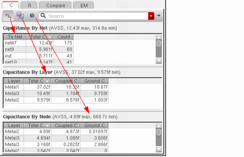 By default, the rows are displayed in the decreasing order of values in the Total C column of a table. However, if constraints are applied to check capacitance values on nets, the nets with violating constraints are displayed on top to bring them in focus, as shown below.You can use the Search field to filter capacitance details for selected nets. Alternatively, you can use the filter command on the EAD Browser to view details for only selected nets, or the nets with constraints, or violated constraints. For more details on filters, refer to Filtering Rows.
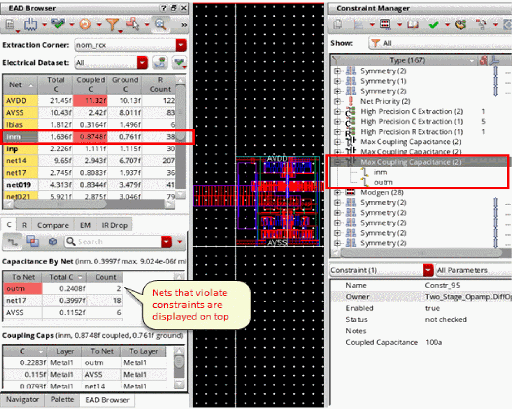
If Automatically zoom display to selected network or parasitic is switched on, the display automatically pans and zooms to the selected nodes. -
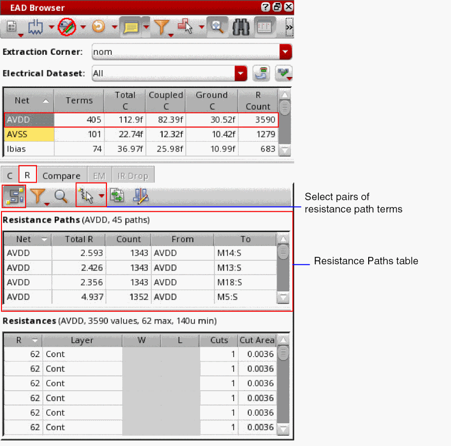
The R tab shows the terminal-to-terminal resistance paths for the net selected in the summary pane. For each resistance path, the total resistance value, R count, and the names of from and to terminals are displayed. Clicking on a row in the Resistance Paths table shows the list of resistances on this path in the Resistances table, as shown below.
Important Points to Note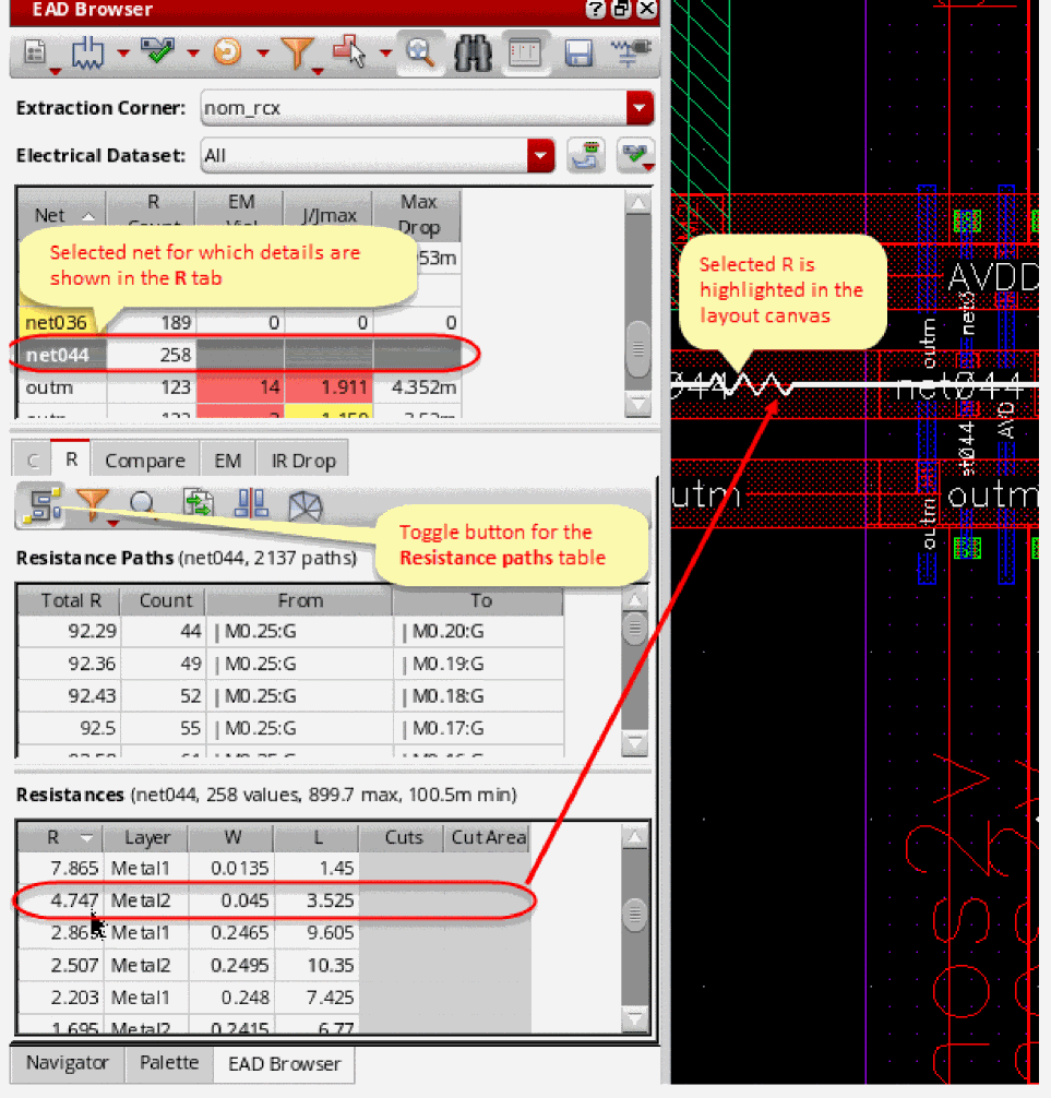
-
If the Detailed Parasitic Tables check box on the Environment tab of the EAD Setup form is selected, by default, the R tab shows only the Resistances table. Click
 on the toolbar of the R tab to show the Resistance Paths table that lists all the resistance paths for a net.
 -
If the number of resistors on a particular net exceeds the value specified by the resPathsResistorLimit environment variable, EAD resolves only a limited number of resistance paths. For the remaining paths, the Total R and Count columns show
Click to Resolve. You need to resolve the remaining resistance paths manually. - When you select a net in the summary pane and the Resistance Paths table is displayed, EAD looks for the resistance paths for that net. If resistance paths are found for the net, it displays all the available paths in the table. After that, it calculates resistances and displays the values in the Total R and Count columns.
-
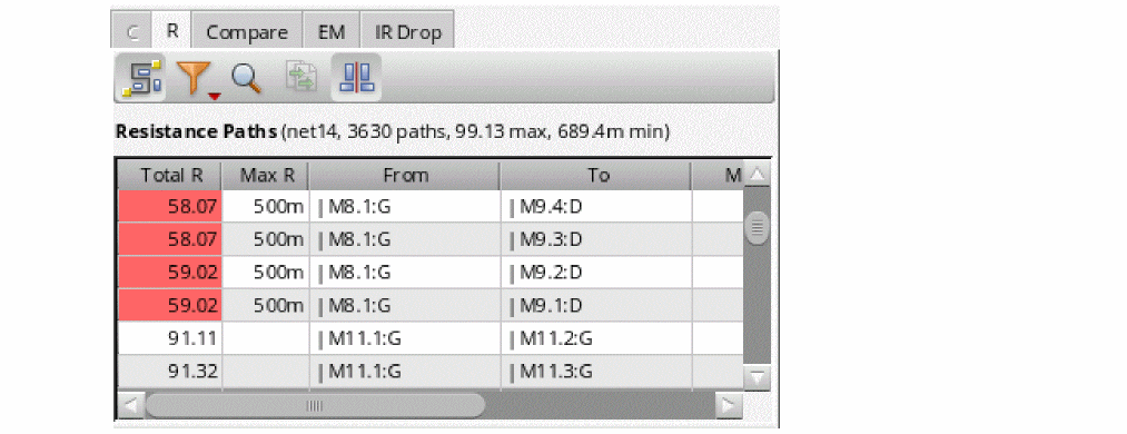
If the Max Resistance constraint is applied between two terminals or instance terminals on the selected net, EAD verifies the constraint. It highlights the resistance paths where the total R between those terminals or instance terminals exceeds the maximum resistance value specified by the constraint. All the paths violating the Max Resistance constraint are displayed on top of the table, as shown below.If the Max Resistance constraint is applied on a single member (terminal or instance terminal), EAD finds paths to all other terminals or instance terminals on that net, and highlights those paths where total R exceeds the maximum resistance value.
- If the Max Voltage Drop constraint is applied on a single member (terminal or instance terminal), EAD finds paths to all other terminals or instance terminals on that net, and highlights those paths where total voltage drop exceeds the maximum voltage drop value.
-
If you want to view the maximum possible current on each resistance path in the Resistance Paths table, you can show the hidden Max Current column by selecting the name of this column in the context-sensitive menu of the column headings. This column shows the maximum current limit possible for a resistance path over all active datasets. The tooltip of the column shows the name of the dataset for which this maximum current limit is calculated.
The command to display the Max Current column is not available for the nets with high-precision resistance enabled. -
For a large net with many terminals, the number of resistance paths could go into thousands or more, and the resolution all the resistance paths can be time consuming. In such cases, the tool might become unresponsive until this is done. To avoid this, EAD allocates only a limited time to this activity of calculating the resistance paths. This time limit is specified by the resistancePathsTableTimeout environment variable. By default, this variable is set to
2(seconds), but you can reset it to the duration you want the tool to spend on reading the resistance paths in your designs. If you set this variable to 0, the time limit is removed.
If the resistance paths search process is taking a long time, EAD displays the progress on the status bar of the Virtuoso Layout EAD window. If required, you can interrupt the process at any time by pressingCtrl+C. -
It is possible that for large designs, EAD does not identify all the resistance paths for the selected net in the allocated time. If you do not see the path of your interest listed in the Resistance Paths table, you can search for it using the search feature. For this, click
 on the toolbar of the R tab. The From and To fields are displayed at the top of the table, as shown below.Depending on your requirement, enter the name of instance terminal in the From and To fields. You can use wildcard characters to specify the instance terminal names in the these fields. When both from and to terminal instance names are given, the tool searches for the resistance paths between them. However, if either of these values is given, the paths from or to the specified instance terminals are displayed.
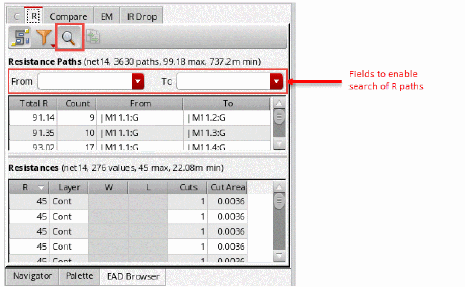
-
If all the resistance paths are not resolved within the time limit set by resistancePathsTableTimeout, the Resistance Paths table shows only the from and to instance terminal names. The Total R and Count columns show
click to resolve, as shown below.In this case, there are two ways to resolve resistances: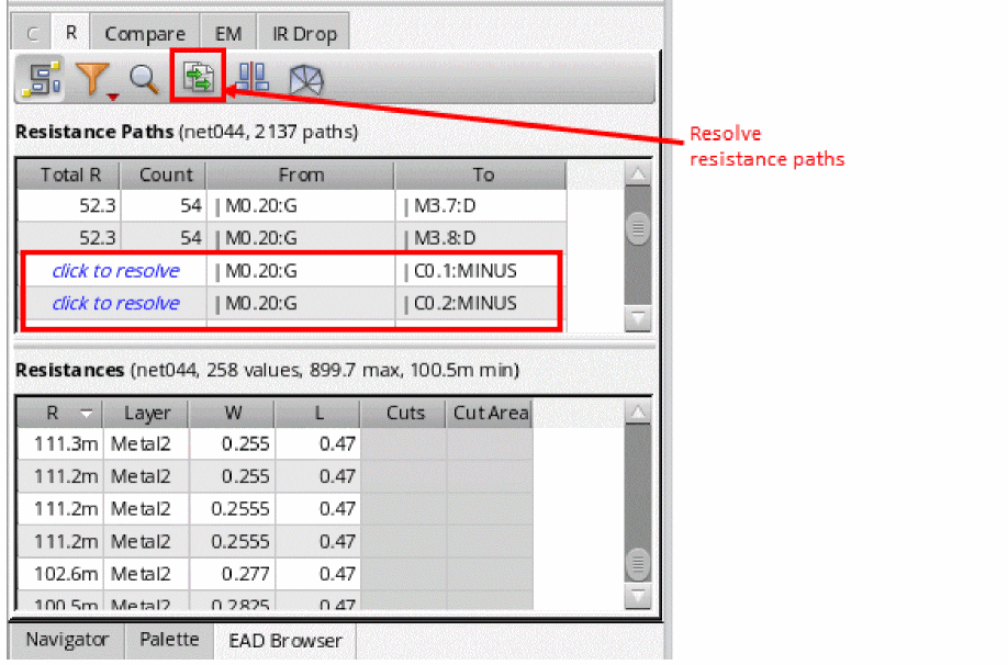
- Paths with constraints are given higher priority. They are always solved and displayed at the top.
-
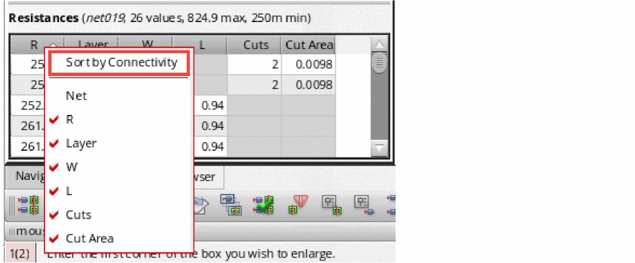
By default, the resistance values in the R column of the Resistances table are displayed in the order in which they are connected in the resistance path. You can display the rows as per the ascending or descending order of the values displayed in any column by clicking the corresponding column header. To restore the default order, right-click a column header and choose the Sort By Connectivity command.
-
Use the options of the Select which layers are displayed in the table command on the toolbar to show or hide rows for selected layers. This command is visible when either the detailedParasiticTables environment variable is set to
tor the Detailed Parasitic Tables check box is selected on the Environment tab of the EAD Options form.
-
If the Detailed Parasitic Tables check box on the Environment tab of the EAD Setup form is selected, by default, the R tab shows only the Resistances table. Click
-
The Compare tab shows the maximum difference and the % error between the values on two or more selected nets. Clicking on a net in the Coupling Capacitance by Net table highlights the net in the layout canvas.
For more information on the C, R, and Compare tabs, see Viewing and Analyzing Parasitics and Comparing Parasitic Values for Multiple Nets.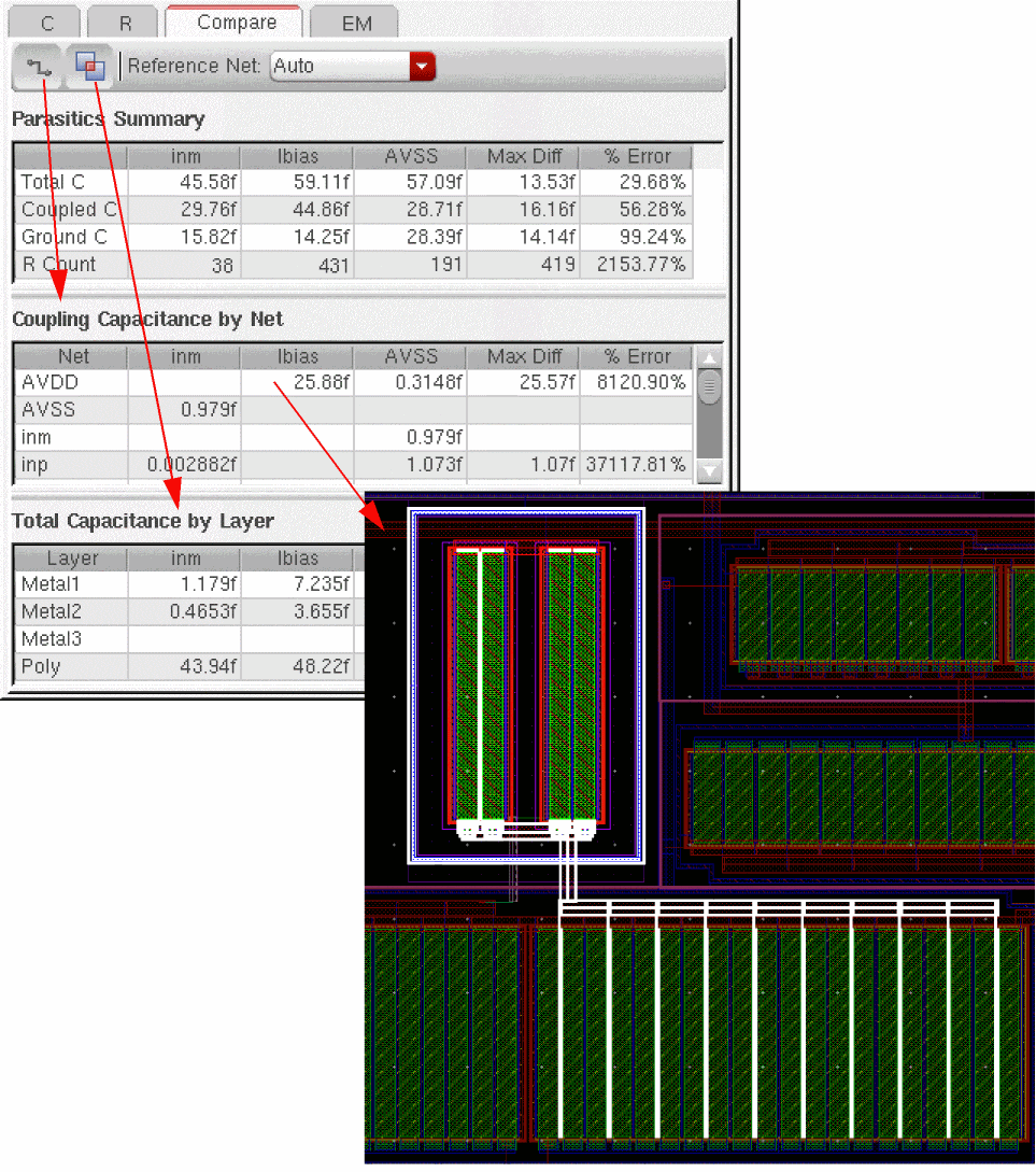
-
The EM tab shows any electromigration violations present for the net selected in the summary pane. The color coding is controlled by EM Violation Highlighting settings in the Extraction tab. If there are no violations for the selected net, the table is empty.By default, EAD displays only those resistors with violations in the EM tab (i.e., those that have a ratio of J/Jmax greater than 1 or the minimum violation level whichever is lower). To see all resistors, set the emResultsShowAllResistors environment variable to
t.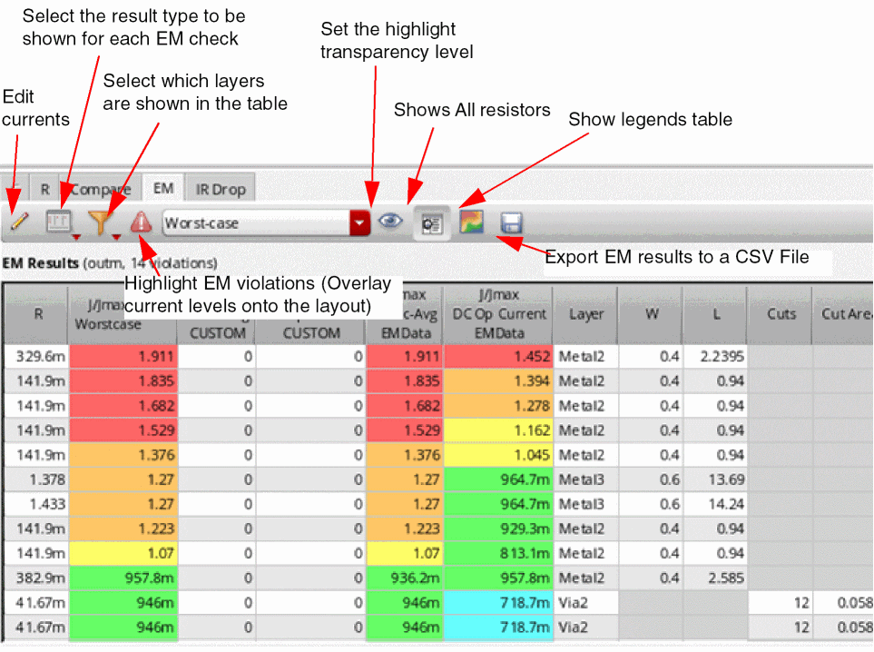 Click the Edit currents button to manually add currents to the CUSTOM dataset in cases where there is no current data available from ADE Assembler. You can also save the dataset with a user-defined name. See Running EM Checks on a CUSTOM Dataset for more information.
-
Click the Result type command to control what values are displayed in the EM table.
- You can set the emTableResultType environment variable to set the value to be displayed by default.
- Click the Select which layers are displayed in the table command and select one of the following options to control which layers are shown in the EM table.
-
Choose a Highlight overlay to apply to current values for the selected nets.
An overlay color-codes the currents calculated for the selected nets based on the EM information available for that net and the violation highlighting colors defined in the legend table for the EM tab.
Use the Highlight Transparency slider to change the transparency of the violation highlighting in the canvas. For example, you might increase the transparency to make it easier to see the underlying geometry.
See Highlighting and Fixing Violations in the Layout Window for more information. -
Use the Export Results to a CSV File command to save the results from electromigration analysis for the selected net into a CSV file.
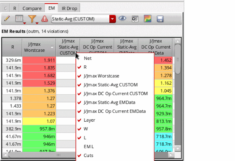
-
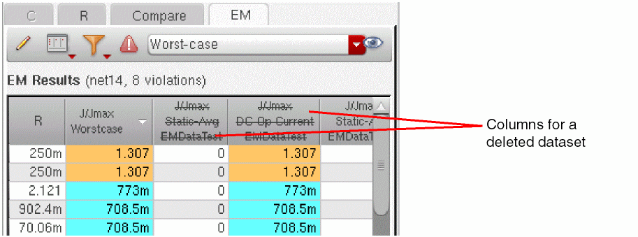
Change the columns shown in the EM results table by clicking the right mouse button in any column header, and selecting or clearing the check box next to the information you want to show or hide.If any dataset has been deleted from the constraint view, the column header corresponding to that will appear in the strikethrough font style. You can remove such datasets from this list by using the Delete Electrical Data command on the EAD toolbar.
-
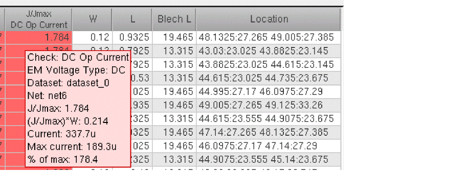
Move the pointer over any cell to see more information about the value shown in that cell.
-
Click the Result type command to control what values are displayed in the EM table.
-
The IR Drop tab shows the voltage drop details between different source and sink terminals connected to a net. The source and sink terminals are determined based on the direction of current for different terminals or instance terminals.
When you extract parasitics and run EM check, the maximum voltage drop value for each net is displayed in the Max Drop column of the summary pane. Click in a cell in this column to view the IR Drop data across different parts of the selected net on the IR Drop tab in the details pane. The figure below shows an example of IR drop data fornet14.
The IR Drop tab shows two tables: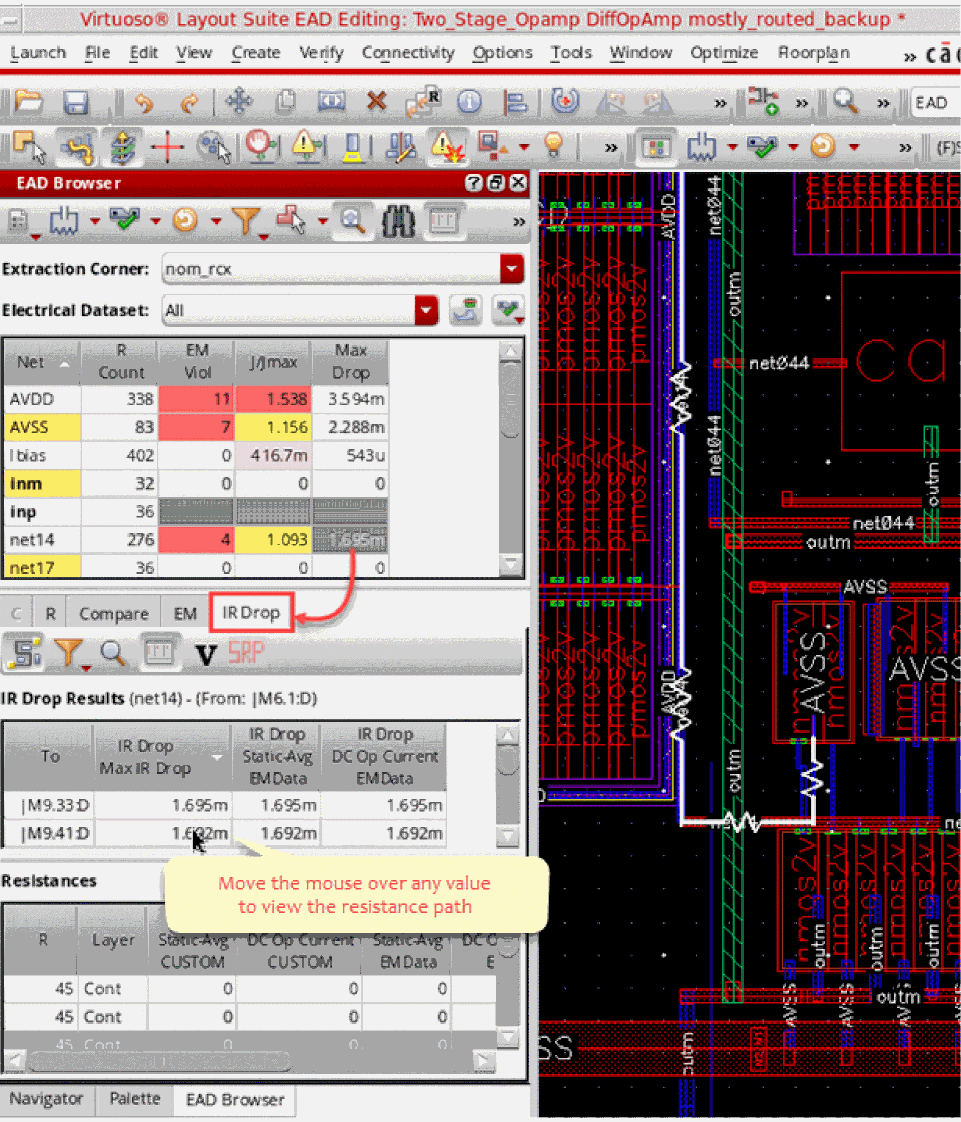
- IR Drop Results: Shows for each dataset and current type the IR drop value between a pair of pins or instance terminals, or between a pin and an instance terminal. In this table, you can move the mouse over any value to highlight the resistance path on the layout canvas.
-
Resistances: Shows IR drop for all resistor values for a path. When you click on a cell in the Max Drop column in the Summary pane, this table shows IR drop for all the resistances on the selected net. When you click on a particular row in the IR Drop Results table, this table shows IR drop for all the resistances between the instance terminals specified in that row. The header of the Resistances table is also changed to show the terminal names and total resistance between them, as shown in the figure below.The SRP (Shortest Resistance Path) icon on the IR Drop tab appears dim. This icon becomes available only when a resistance path is selected in the Resistances table.
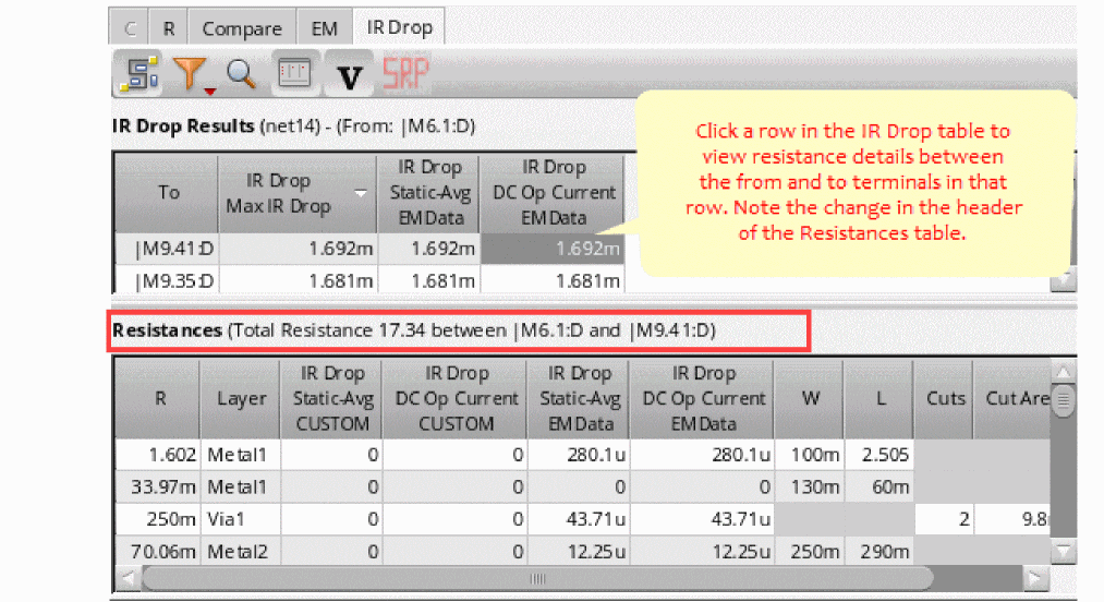
You can click SRP to filter the Resistances table to selectively view only those resistors that are in the shortest resistance path.The Resistances table is visible only when the detailedParasiticTables environment variable is set toNote the following points for the IR Drop Results table:tor the Detailed Parasitic Tables check box on the EAD Options form is selected.- IR drop from each available dataset is shown in a separate column, so the number of columns displayed may vary.
-
When the from or to instance terminal or pin names are the same for all rows, the corresponding column is hidden and its static value is displayed on top of the table. For example, in the figure given above, the from instance terminal is the same for all rows, so it is displayed at the top
(From: |M6:1:D). If required, you can show the From or To column by using the table header context menu. - The Max IR Drop column shows the worst-case IR drop across all datasets for each pair. The rest of the columns show the IR drop data for each type of analysis from the selected datasets.
- By default, the results are displayed in decreasing order of max IR drop value across all datasets. However, you can sort the results in ascending or descending order of the values displayed in any column by clicking on the corresponding column header.
- Move the mouse over any path in the IR Drop table to highlight the path in the layout canvas.
- You can view the From Location and To Location columns to display the location co-ordinates of the from and to terminals of the resistance path, as well as the name of the layers enclosing them.
- These columns are hidden by default. Choose the From Location and To Location commands from the context-menu of the IR Drop table header to view these columns.
When you select any cell in these two columns, EAD highlights the boundary of the enclosing conductor for the from or to terminal, as shown below.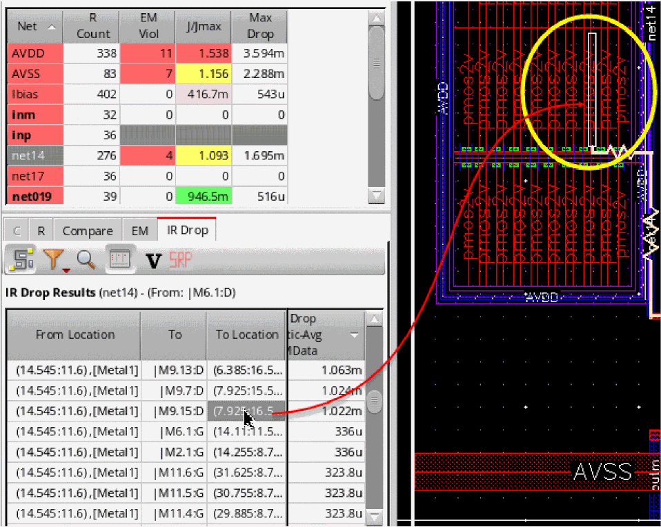
-
You can search for a specific IR drop path on the net selected in the summary pane by using the Find a specific IR Drop path (
 ) command on the IR Drop toolbar. When you click this command button, the Terminal Name drop-down list is displayed on the IR Drop tab. This list shows the names of all the terminals on the selected net. Select a terminal from this list to view all the IR drop paths from or to that terminal.
 - Use the Toggle IR Drop Table command on the toolbar of this tab to show or hide the IR Drop Results table.
-
Use the options of the Select which layers are displayed in the table command on the toolbar to show or hide rows for selected layers. This command is visible when either the detailedParasiticTables environment variable is set to
tor the Detailed Parasitic Tables check box is selected on the Environment tab of the EAD Options form. -
When the IR Drop results are generated for Fast R extraction, you can overlay the IR drop data on the layout canvas. This gives a visual evaluation of voltage drop across the net in reference to the selected terminal for the given current type and dataset combination. To overlay the data use the Highlight IR Drop on Canvas and Show Highlight Legend (
 ) command on the toolbar of this tab. Layout EAD hides the tabular voltage drop data and displays a highlight legend. The color codes from this legend are used to show the heat map, that is, to overlay the voltage drop at different points on the selected net, as shown below.You can customize the numbers of bins of the range for the bins in which you need to categorize the IR drop data and view the heat map on the layout. For this, to edit the number of bins, edit the value in the Number of bins spin box. The highlight legend is modified accordingly to reflect the required number of bins. For example, in the figure shown below, the data is categorized in only four ranges.
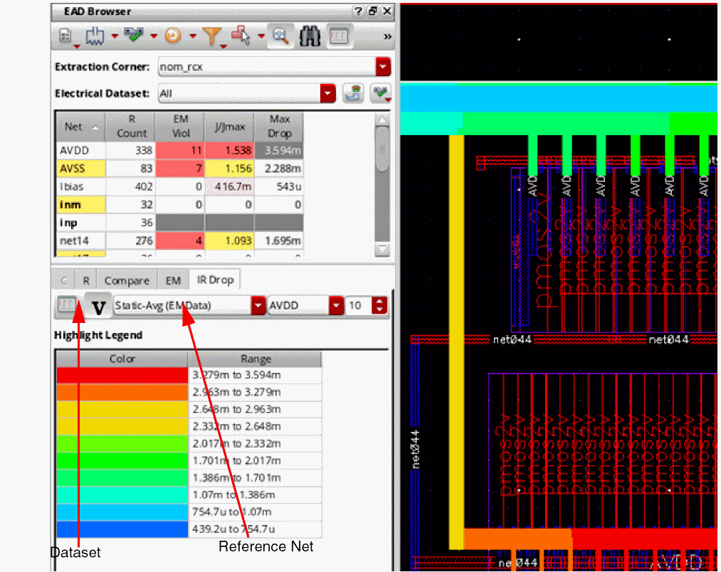 You can also change the color to be used for a particular range. For this, double-click a cell in the Color column of the Highlight Legend table, and choose a highlight color for the corresponding range, as shown below.
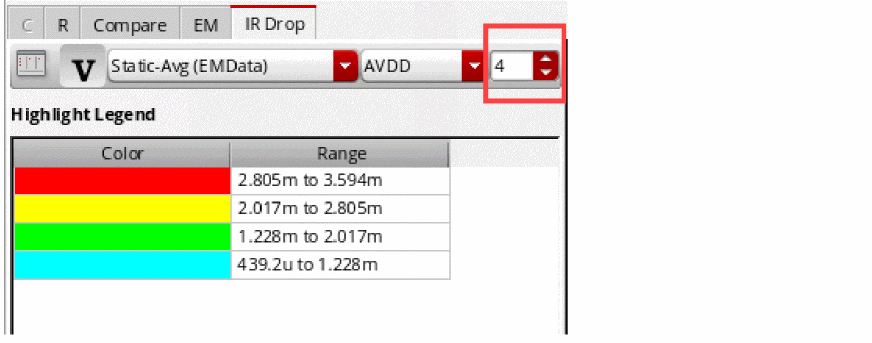 The overlay on the layout is also updated to reflect the change.
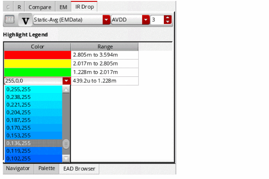
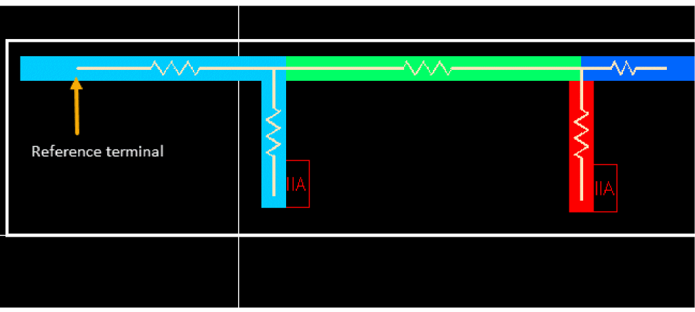
If multiple datasets are available, you can select any dataset for which you want to overlay the voltage drop information on canvas. You can also change the terminal to be used as reference for voltage drop calculation across the net. When you change the reference terminal or the dataset and current-type combination, the voltage drop values are recalculated and the overlay is changed. The highlight legend is also dynamically changed depending on the high and low range of voltage drop between the reference terminal and other terminals.
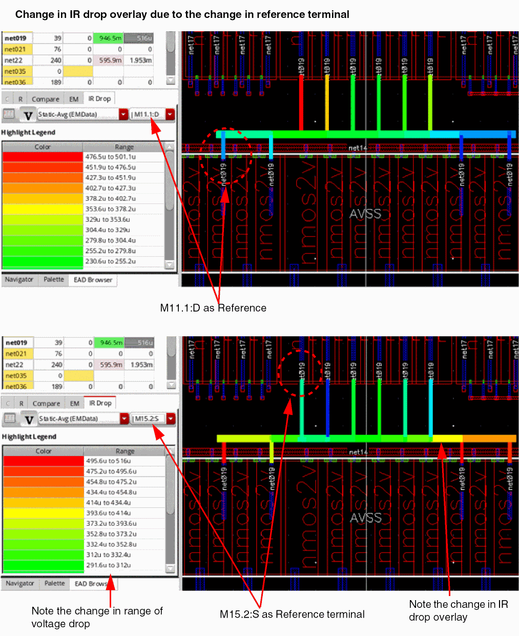
The following example shows the changes in IR drop overlay fornet19according to the change in reference terminal.
-
You can view the voltage drop overlay and tabular data at the same time. For this, click Highlight IR Drop on Canvas and Show Highlight Legend (
 ) on the toolbar to enable overlay, and then click Show/Hide IR Drop Results Table(
 ).
). - You can apply layer filters to view the voltage drop overlay on selected layers. For this, perform the following steps:
-
Set the detailedParasiticTables environment variable to
t. This will display the Selects which layers are displayed in the table ( ) icon on the toolbar of the IR Drop tab.
 -
Set the applyLayerFilterOnCanvasHighlight environment variable to
t. -
Click Highlight IR Drop on Canvas and Show Highlight Legend (
 ) on the toolbar to enable overlay.
 -
Click Show/Hide IR Drop Results Table(
 ) to view the other commands on the toolbar.
 -
Click (
 ) and select a layer from the drop-down list of layer names.
The voltage drop overlay is displayed only for the selected layer. You can select multiple layer names to view the overlay for the together.
Viewing Resistance Paths between Terms
You can use the Select pairs of resistance path terms options to filter resistance paths between the selected terms in the Resistance Paths table.
To view resistance path between the selected terms:
- Select a net in the Summary table and click the R tab.
-
Click the Toggle resistance path table
 icon to display the Resistance Paths table.
-
Click the drop-down arrow in the Select pairs of resistance path terms icon and select one of the following options:
-
Select From-To Term Pairs: To filter resistance paths between the From and To terms, first select the From term and then select the To term in the schematic.
The resistance path between the selected From and To terms is displayed in the Resistance Paths table and the path is highlighted in the schematic.
The following example shows the results whenM10:sandM0:sare selected as the From and To terms in the schematic, respectively.You can now select different pair of From and To terms in the schematic to filter the resistance path in the Resistance Paths table and highlight the resistance path in the schematic. Note that when using the Select From-To Term Pairs option, both From and To terms are reselected. Press the Esc key to exit selection mode.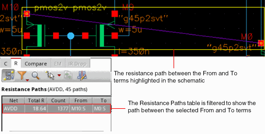
- Select From Term and Multiple To Terms: To filter resistance paths between a single From and multiple To terms, first select the From term and then select the To term in the schematic. If you again select a term in the schematic, only the To term changes. The first term you selected in the schematic remains selected as the From term. Press the Esc key to exit selection mode.
-
Select Path to Topmost Term: To filter the resistance path from the selected instance term to the topmost term in the hierarchy. First, descend into a cell and then select the instance term that is connected to a term present in the higher level of hierarchy.
The resistance path between the selected instance term and the topmost term in the hierarchy is displayed in the Resistance Paths table and the path is highlighted in the schematic.
-
Select From-To Term Pairs: To filter resistance paths between the From and To terms, first select the From term and then select the To term in the schematic.
Changing Data Display in the EAD Browser
This section describes how to change the way data is displayed in the EAD Browser tables.
Toggling Dual Pane and Single Pane View
You use the Toggle dual pane view button on the EAD Browser toolbar to toggle between the default dual pane EAD Browser view and a single pane view.
Dual pane view is the default and features the summary table on top and the detail table underneath. Single pane view has all tabs listed in a single panel.
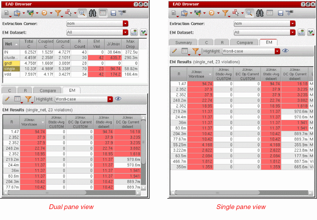
In dual pane view, when you click a value cell in the summary table, the relevant corresponding tab is opened in the detail table. For example, if you click the EM Viol cell for vdd in the summary table, the EM tab is opened in the detail table and the violation details for vdd are shown. Similarly, if you press the Ctrl key and select two nets in the summary table, the Compare tab is opened in the detail table.
Use single pane view when you need to focus on the results of a single net and need more space to view the results more comfortably.
Sorting Columns
You can change how data is sorted in columns and also in which position in the table a particular column appears.
-
Click once in a column header (for example R Count) to sort the column in ascending order.
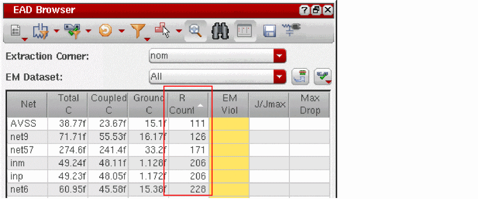
-
Click again to sort the column in descending order.
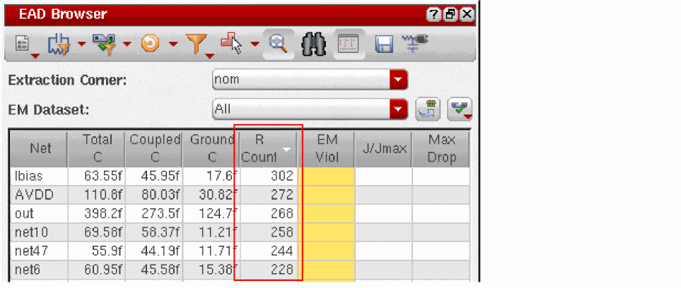
- Click-and-hold the column header and move your mouse to drag the column to a new location.
-
Release the mouse button to drop the column at its new location.
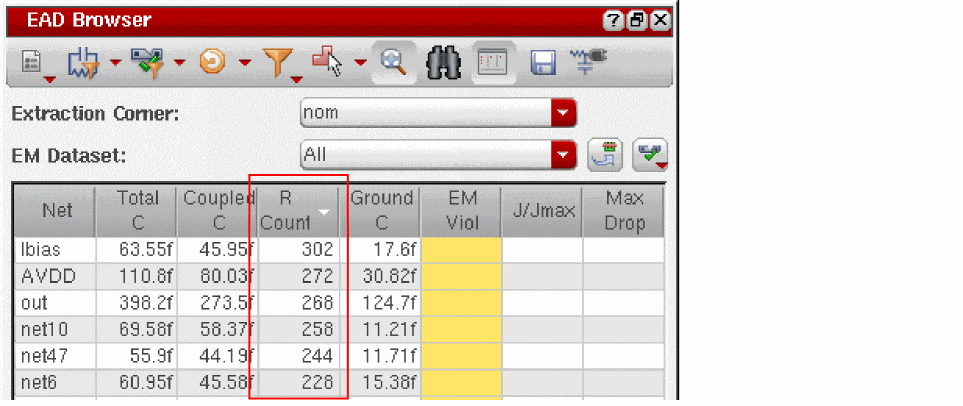
Showing and Hiding Columns
To specify which columns are visible in a table,
-
Right-click in any column header.
- Select or deselect the check box next to the column you want to show or hide.
Filtering Rows
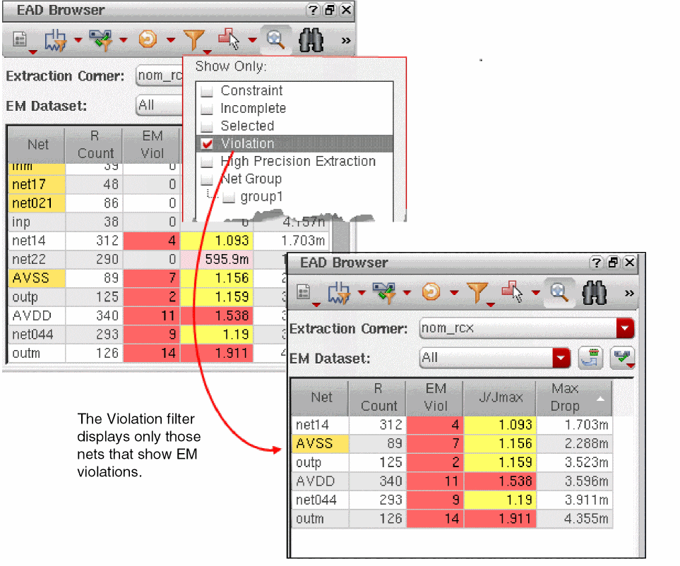
By default, all available nets are displayed in the summary pane. You can use the Filtering options to show only the nets for which you need to analyze parasitic details and EM violations.
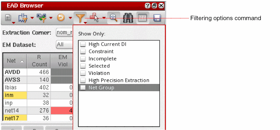
Click Filtering options on the toolbar and select one or more of the following filtering options to show only those nets that meet the selected criteria.
- High Current DI shows information about the nets on which you have defined the HighCurrent design intent. Also see Creating a HighCurrent Design Intent.
- Constraint shows information about the nets on which you have defined electrical constraints other than the High Current design intent. Also see Extracting Parasitics in Layout EAD.
- Incomplete shows information only for the nets with incomplete parasitic network.
- Selected shows information about the nets selected on the layout canvas. When this filtering option is selected, click the nets in the layout canvas to show their details in the summary pane.
- Violation shows information about the nets that violate electrical constraints and/or EM limits.
- High Precision Extraction shows information about only those nets for which you have enabled High Precision R Extraction or High Precision C Extraction. Also see Extracting Parasitics in Layout EAD.
-
Net Group shows information only about those nets that you have included in the specified net groups. When selecting this filter, you also need to select the net groups for which you need to view the information. Also see Creating Net Groups.
The following example shows how the Violation filter is used to display the nets with violations.
Creating Net Groups
You can create net groups to group similar types of nets together. This also helps in filtering nets that belong to a particular net group.
To create a net group, perform the following steps:
-
Right-click one or more nets in the summary pane of the EAD Browser, and choose Net Groups – Add to New Group.
The EAD – New Net Group form is displayed. - Enter a name for the new group in the Net Group Name field.
- Click OK to close the form.
A new net group is created with the given name and the selected net(s) are added to the specified net group. The name of the net group is added to the Net Groups menu in the context-sensitive menu for the nets.
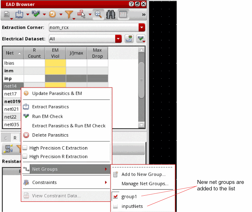
To add a net to an existing net group, select a net and choose Net Groups – <name of the existing net group>.
Managing Net Groups
You can delete or merge net groups by using the Manage Net Groups command.
Deleting Net Groups
To delete a net group, perform the following steps:
-
Right-click in the summary pane of the EAD Browser and choose Manage Net Groups. The EAD - Manage Net Groups form is displayed.
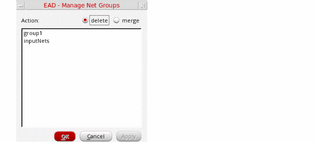
- Select a group name from the list of groups.
- Ensure that the delete action is selected.
- Click OK.
The selected net group is deleted.
Merging Net Groups
To merge multiple net groups, perform the following steps:
-
Right-click in the summary pane of the EAD Browser and choose Manage Net Groups. The EAD - Manage Net Groups form is displayed.
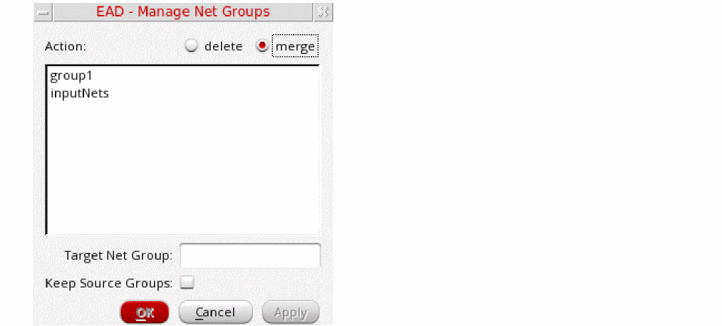
- Select two or more group names from the list of groups.
- Select that the merge action.
- In the Target Net Group field, specify a name to be given to the new or target group that will contain the nets from the merged net groups.
- If you need to retain the existing groups that are being merged, select the Keep Source Groups check box.
- Click OK.
A new net group is created with the nets from the selected net groups.
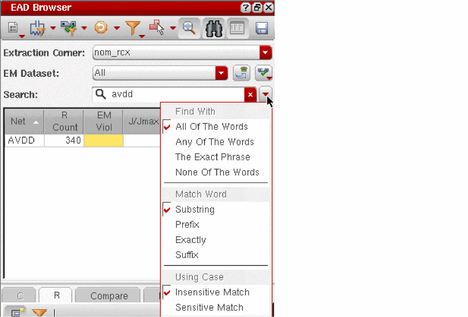
Searching Nets
To search for a particular net and to view results, use Search.
-
Click Search in the EAD Browser toolbar.
The Search drop-down list is added to the panel above the summary pane.
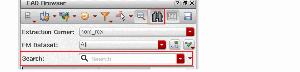
-
Type in the name of the net for which you are searching.
Alternatively, you can select a net name from the search history in the drop-down list, if available.
While you type in a name, all the net names that contain the search string get listed in the summary pane dynamically.
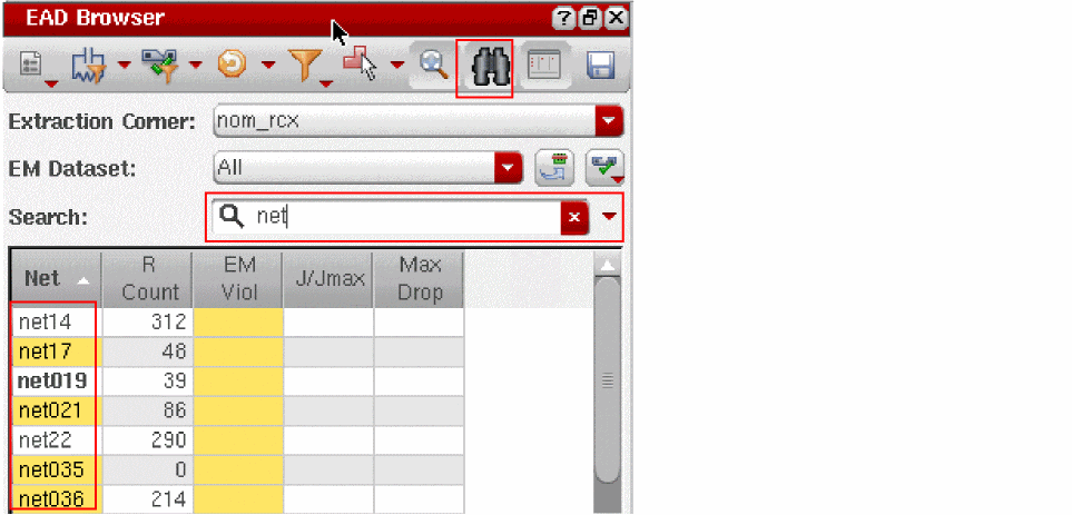
- Select the desired net name in the summary pane and view the results in the details pane.
-
You can customize the search by using the search settings available in the drop-down menu next to the Search drop-down list, as shown below.
Managing EAD Setups
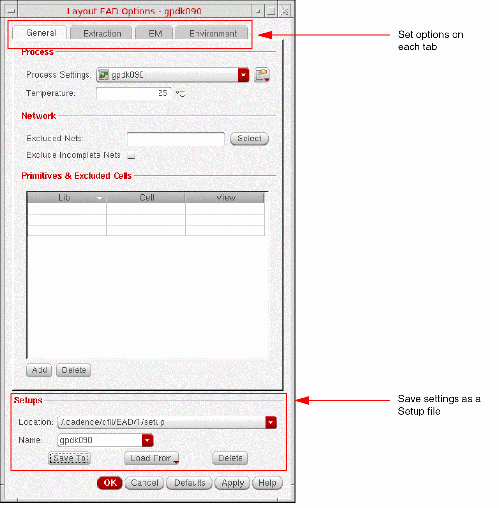
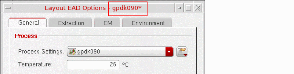
You use the Layout EAD Options form to define the setups required to drive parasitic extraction and EM analysis in Layout EAD. A setup includes a pointer to the process settings required for parasitic extraction and EM checking, as well as user-customizable tool options. When you have specified the options you require, you can use the controls in the Setups section at the bottom of the form to save them in the system for later use.
You might typically define two EAD setups; one for use in EM analysis and one for parasitic extraction to be used in resimulation:
- For EM analysis, you need extract only R parasitics and include the shapes inside devices and Pcells
- For resimulation, you would typically perform both R and C extraction, and extract device and Pcell shapes (because these are already modeled in simulator models)
Preparing an EAD Setup
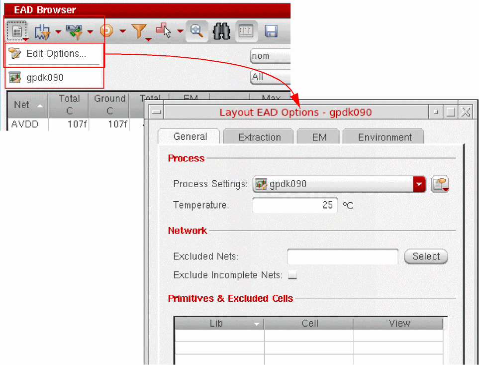
-
Choose Options – Edit Options from the EAD Browser toolbar to open the Layout EAD Options form.
Alternatively, choose EAD – Options from the Layout EXL menu bar.
-
Set the options on each of the four tabs to meet your requirements.
-
General lets you specify the process settings to be used in the current session, the extraction temperature to be used, and the nets and cells to be excluded from parasitic extraction. See General for more details.
If you need to change the process settings for your design, see Editing Process Settings. - Extraction lets you specify the main extraction engine controls, resistance and capacitance thresholds, and high precision C and R extractor settings. See Extraction for more details.
- EM lets you specify the settings to be used for electromigration checking, including temperature, default and minimum current values, scaling factor, and lifetime values. See EM for more details.
-
Environment lets you specify how violations are highlighted and control whether nets highlighted and selected in the EAD Browser are also highlighted and selected in the layout view. See Environment for more details.You can specify default values for each of the options on the form using the environment variable associated with the option in question. See Appendix A, “Form Descriptions” to see the environment variables for each option and Appendix B, “Environment Variables” for a complete list of all EAD-related environment variables.
-
General lets you specify the process settings to be used in the current session, the extraction temperature to be used, and the nets and cells to be excluded from parasitic extraction. See General for more details.
Saving an EAD Setup
When you have set the options to meet your requirements, save the setup so that you can use it during your analysis of the current design.
Saving a Setup
To save the current settings to the currently loaded setup file,
- Choose the required Location and Name from the pull-downs in the Setups section at the bottom of the form.
-
Click Save To.
The setup file is saved with a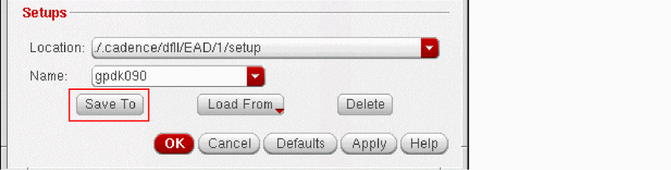
.inifile extension to the specified location; for example:/.cadence/dfII/EAD/1/setup/gpdk090.ini
Creating a New Setup
-
Type the new Name into the editable field.
-
Click Save To.
The new setup file is saved to the Location specified in the form and added to the list in the Options menu in the EAD Browser toolbar.
Referencing a New Setup
To use the new setup in the current design session,

Loading an EAD Setup
You can also load settings from an existing setup file into the Layout EAD Options form, edit them to meet your requirements, and then save them as a new setup.
When you load a new setup that maps to the same extraction corner (ICT file mapping), then all of the nets in the design are marked as modified and requiring re-extraction. If you load a new setup that maps to a different ICT file, then the parasitics are read and loaded into the EAD Browser and the graphical user interface is reset to its default state.
To load a different EAD setup,
-
Choose the Location and Name of the setup you want to load.
The list of locations includes all the
.cadencedirectories found in the paths specified in the Cadencesetup.locfile and in any additional directories specified by the auxSearchPaths environment variable. Also listed are any technology-dependent setup files stored in a subdirectory with the same name as the technology library for the design. -
Click Load From to update the form with the values from the specified setup file or hold down the button to see a drop-down list of all the setup files stored for the design.
The specified setup is loaded and any stored parasitic information is retrieved and loaded. No extraction or EM checking is run by default, however, if the data exists, it is automatically loaded as well.
The form title updates to show the name of the loaded setup file.
As soon as you make a change to the loaded setup, the form title displays an asterisk to show that there are unsaved changes.
- Click Save To to save the changes in the setup file.
When EAD is initialized using the setup information, it checks whether the specified EM data source file (EM data file, ICT file, ICT-EM file, or iRCX-EM file) exists and is readable. If the file is not found or is not readable, it displays an appropriate warning message. To disable the display of this warning message, either click Do not show again on the message box or set the warnWhenEMDataSourceIsInvalid environment variable to nil.
Related Topics:
Editing Process Settings
Process settings contain information about the extraction corners and the models to be used for each during EM checking, the mappings between layers in the ICT file and those in the Virtuoso technology file, and how vias and shapes in sub-cells are handled during extraction.
For details about the process information contained in the ICT technology file and the syntax of the commands, see Chapter 3 in the
To edit the process settings for a design,
-
Click Process Settings menu (
 ) and choose Edit to open the EAD Process Settings form.
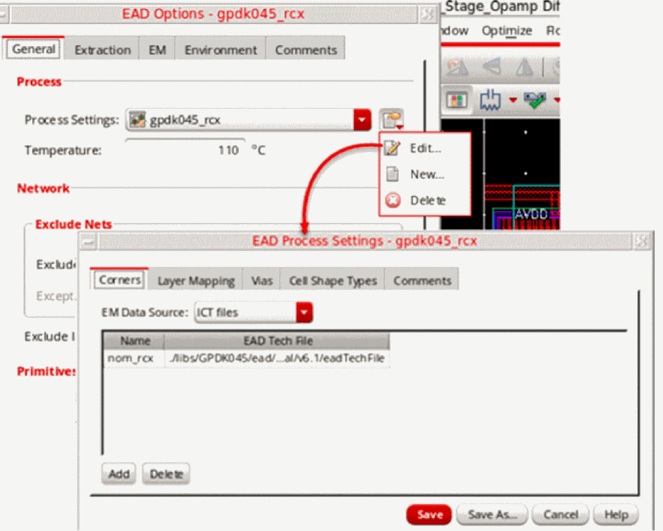
-
On the Corners tab of the EAD Process Settings form, choose an EM data source from the EM Data Source drop-down list. See EAD Process Settings – Corners for more details.
Also see: Using Custom Variables in ICT-EM Files -
Edit the process settings on each tab to meet your requirements:
- Corners is where you associate your extraction corners with the ICT file or eadTechFile to be used for extraction. The EM Data Source field lets you specify the source of the EM models and rules; either a Virtuoso technology file, an ICT-EM file, or an EM data file. See EAD Process Settings – Corners for more details.
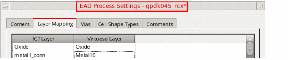
- Layer Mapping lets you specify how the layers used in the ICT file map to the layers defined in the Virtuoso technology file. See EAD Process Settings – Layer Mapping for more details.
- Vias lets you specify how vias are flattened and clustered. See EAD Process Settings – Vias for more details.
- Cell Shape Types lets you control how shapes in sub-cells contribute to parasitic extraction. See Overview of Parasitic Extraction in Layout EAD for more information.
- Comments lets you view and modify the comments saved in the process settings file.
As soon as you make a change to the process settings, the forms title displays an asterisk to show that there are unsaved changes.
-
When you have finished, do one of the following:
-
Click Save to save the settings under the current Process Settings file name.
- Click Save As to save the settings under a different Process Settings name
The process settings file is saved is saved with a.inifile extension to the specified location; for example:/.cadence/dfII/EAD/1/process/gpdk090.ini
You can then use these settings in your current design or in future EAD sessions.
Related Environment Variables
Important Points to Note- If multiple corners are specified, you must ensure that all of the technology files were consistently generated for R-only or RC extraction. A mix of R-only and RC technology files is not supported.
- If the EM data source is an EM data file, the EAD parser ignores the unsupported keywords and parameters. For each ignored keyword or parameter, a warning is displayed in the CIW.
-
Click Save to save the settings under the current Process Settings file name.
Using Custom Variables in ICT-EM Files
If the EM calculations in the ICT-EM file are using certain variables that you would need to modify before running EM checks, you can register those variables with EAD by using the eadRegisterCustomEMVariable SKILL function. Later, you can modify those values by using the eadSetEMVariable SKILL function and then run EM extraction to use the revised variable value for EM calculation.
Checking Layer Mapping
layoutEAD.gui hideCheckLayerMapping to nil to display this check box in the Options menu of the EAD Brwoser.After you load the setup from an EAD setup file, the Check Layer Mapping commands is added to the Options menu on the EAD toolbar.
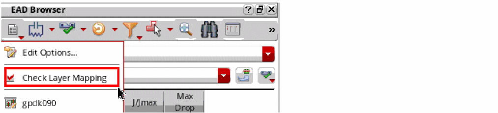
Use this command to check whether mapping of all the layers in Virtouso technology file to the layers in the ICT file is complete. If any layer is found as unmapped, an error is displayed reporting a list of unmapped layers. In such a case, you can update layer mappings on the Layer Mapping tab of the EAD Process Settings form. While you are editing the layer mappings, you can use the Check command on the Layer Mapping tab to rerun the checks. Ensure that there are no warning messages.
Deleting an EAD Setup
To delete a setup that you no longer require:
-
Choose the Location and Name of the setup you want to delete.
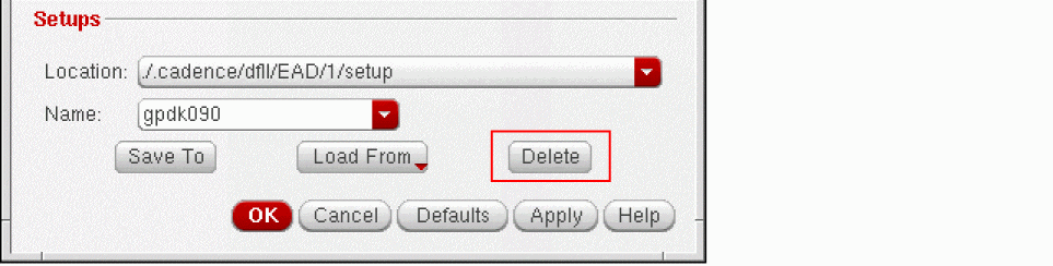
-
Click Delete and confirm the action in the pop-up message that appears.
The setup file is deleted from the location on disk.
Working with EAD States
This section describes how to save, restore, and load an EAD state.
Saving an EAD State
Follow these steps to manually save the current EAD state:
-
On the EAD Browser toolbar, click Save current EAD state. The EAD - Save State form opens.
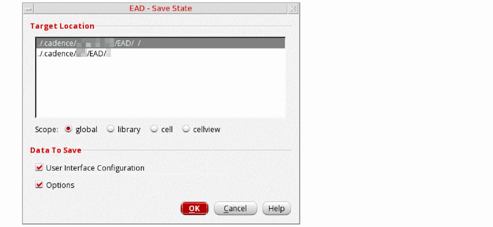
-
In the Target Location section, select a location where you want to save the state data.
The list of locations includes all the.cadencedirectories found in the paths specified in the Cadencesetup.locfile.You can also specify your own directory to save or load an EAD state by setting the statePath environment variable. The directory specified by the environment variable is given priority over those specified insetup.locfile. -
From the Scope options, select one of the following options tag the state being saved for the specific subsets of designs:
- global: Saves the state that can be used for all designs.
- library: Saves the state that can be used for all designs in library of the current design
- cell: Saves the state that can be used for different views of the current design
- cellview: Saves the state that can be used only for the current design
- In the Data to Save section, select the following options to save the specific parts of the EAD state:
- Click OK to save the current EAD state.
Restoring an EAD State Automatically
You can choose to automatically restore EAD to a state in which the design was last exited. Set the saveStateOnClose environment variable to t:
envSetVal("layoutEAD.gui" "saveStateOnClose" 'boolean t)
Loading an EAD State
You can load an EAD state, which has been saved earlier, by clicking Load EAD state on the EAD Browser toolbar. EAD searches for the state data based on the following parameters. The first instance of the state found is loaded.
-
Scope: State data is searched by scope in the following order:
cellview,cell,libraryandglobal. -
Target Location (Path): State data is searched by paths in the order they are defined in the
setup.locfile.
You can also load EAD state data automatically on startup. To do so, set the following environment variable to t:
envSetVal("layoutEAD.gui" "loadStateOnOpen" 'boolean t)
Extracting and Analyzing Parasitics
This section explains how to use Layout EAD to extract and analyze parasitics for a layout design; how to use the EAD Browser to find out more about the reported values; how to compare the values extracted for different nets of interest; and how to extract parasitics automatically while you are editing the layout in the canvas.
- Overview of Parasitic Extraction in Layout EAD
- Customizing Extraction of Parasitics
- Extracting Parasitics in Layout EAD
- Viewing and Analyzing Parasitics
- Comparing Parasitic Values for Multiple Nets
- Using Automatic Update Mode
- Distributed Computation of Extraction Process
- Working with Job Policies
Overview of Parasitic Extraction in Layout EAD
This section describes the default extraction behavior for various design components and explains the settings you can make to change how the extraction is performed.
- Extracting Parasitics on Interconnect Wires Between Devices
- Extracting Parasitics inside Devices
- Extracting Parasitics for Devices and Interconnect
- Extracting Parasitics for Devices and Overlapping Interconnect
- Extracting Parasitics for Local Interconnect Layers
- Extracting Parasitics from Strong, Weak, or Must Connections
- Assigning Shapes for Extraction
- Preventing Extraction Inside Devices
- Stopping Extraction at the Device Boundary
- Specifying the Hierarchy Levels and Hierarchy Shape Type
Layout EAD defines the following types of default capacitance extraction:
-
Coupling capacitance is the capacitance extracted between two shapes with a single net assigned to them; for example,
netAandnetBnext to each other onMetal1.
Net assignment is performed inside Layout EAD by the Layout XL connectivity extractor. - Grounded capacitance is the capacitance extracted between a shape with a net assignment and a shape that does not have a net; for example:
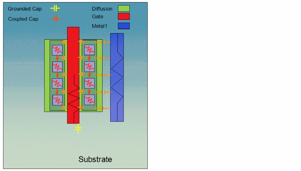
Extracting Parasitics on Interconnect Wires Between Devices
The figure given below illustrates the default extraction behavior for wires used to connect devices:
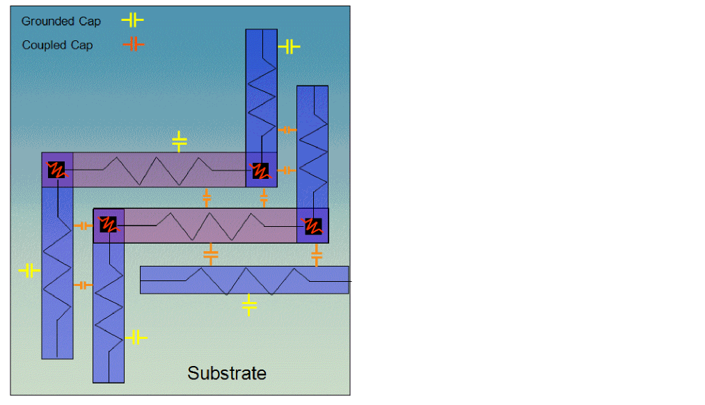
-
Resistance is extracted for all layers defined as
conductorlayers in the ICT file and for vias/contacts (typically poly, contact, and metal layers and vias)
If thelayer_typeis define asdiffusion, resistance is not extracted for that layer. -
Coupling capacitance is extracted between all
conductorlayers (i.e.Metal1toMetal1,Metal1toMetal2, and so on) - Grounded capacitance is extracted between conductor layers and substrate. During resimulation the grounded node is specified in the Parasitics – Setup form.
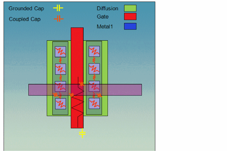
Extracting Parasitics inside Devices
The figure given below illustrates the default extraction behavior inside devices:
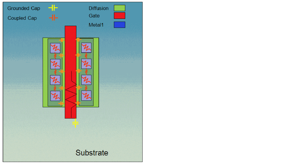
-
Resistance is extracted for the terminals on layers specified as
conductorin the ICT file and for vias/contacts (typically, metal and contacts, but excluding diffusion) -
Coupling capacitance is extracted between all conductor layers (e.g.
Metal1toPoly,Metal1toMetal1, and so on) - Grounded capacitance is extracted between conductor layers and substrate (poly to substrate). During resimulation, the grounded node is specified in the Parasitics – Setup form.
Extracting Parasitics for Devices and Interconnect
When extracting parasitics between devices and interconnect wires, the coupling capacitance is extracted between interconnect outside the device and interconnect inside the device, as shown in the figure given below.
Extracting Parasitics for Devices and Overlapping Interconnect
The figure given below illustrates the default extraction behavior for devices and overlapping interconnect:
-
Coupling capacitance is extracted between interconnect outside the device (defined as
conductorin the ICT file) and interconnect inside the device (defined asconductorin ICT file). - Grounded capacitance is extracted to any shape that has a net, but where the technology file defines no RC extraction on that shape; for example, substrate or diffusion.
Extracting Parasitics for Local Interconnect Layers
When two shapes on different local interconnect layers overlap and also touch by abutment in the vertical dimension, that is, top-to-bottom, the EAD extractor can compute this vertical resistance. Definition for this via is provided in the ICT file. Using the
In no via definition is explicitly drawn, you can leave the ICT via layer unmapped and EAD will compute the resistance from an implied via between the overlapping layers, as shown in the figure below, and calculates a resistance value depending on the area of contact between the two layers.
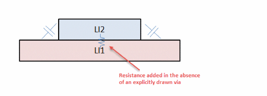
The value of R is displayed in the Resistances table. Since there is no design layer for the via, EAD uses the name of the local interconnect layer for the resistance displayed on the R tab.
Extracting Parasitics from Strong, Weak, or Must Connections
EAD extracts resistance paths between terminals and instance terminals. Depending on the strong, weak, or must pin connectivity, EAD performs R extraction as explained below.
- When different pin shapes are modeled as strong connect, there are multiple figs on a single pin that is further connected to a single instance terminal. In this case, EAD assigns the terminal node to one of the figs and extracts resistance paths to that fig. Multi-finger transistors with internal source-drain strapping should be modeled as strong connect.
- When different pin shapes are modeled as must connect, multiple instance terminals are connected externally, and each instance terminal has a pin and a fig associated with it. In this case, EAD extracts resistance paths to each instance terminal. Multi-finger transistors with no internal source-drain strapping should be modeled as must connect.
- When a pin shape is modeled as weak connect, there are multiple pins on a single terminal. In this case, EAD assigns the terminal node to one of the pins and extracts resistance paths to that pin.
For details on how to set pin connectivity models in the layout, refer to
Customizing Extraction of Parasitics
The following topics describe how you can customize the extraction of parasitics for devices in your layout:
- Assigning Shapes for Extraction
- Preventing Extraction Inside Devices
- Stopping Extraction at the Device Boundary
- Specifying the Hierarchy Levels and Hierarchy Shape Type
- Identifying Instances to be Ignored during Extraction
- Modifying EM Analysis for Wide Pins
Assigning Shapes for Extraction
Layout EAD can treat cells, views, terminals, and layers as different shape types for extraction purposes. This lets you perform a differentiated extraction of terminals on Pcells by defining how non-terminal shapes in sub-cells contribute to the extraction.
Layout EAD recognizes three different shape types:
-
regular – shapes that have a net assignment.
Coupling capacitance is calculated to these shapes. -
background – shapes that do not have a net assignment.
In general, grounded capacitance is calculated to these shapes; however, there is an exception for background shapes on device or instance terminals for which coupling capacitance is also calculated. - invisible – shapes are not sent to the extraction engine.
You specify shape types for the Pcells and instances in your design in the EAD Process Settings form during process setup:
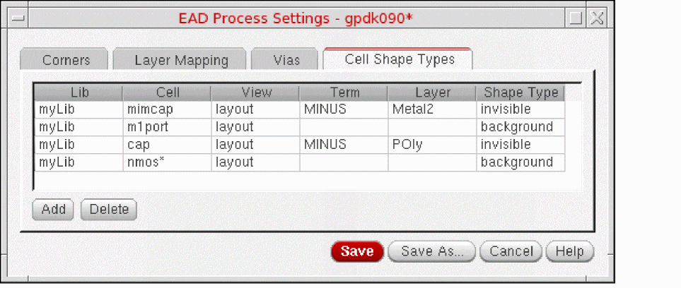
-
Row 1: EAD will not pass the
Metal2shape for theMINUSterminal onmyLib/mimcap/layoutto the extractor because the shape is set toinvisible -
Row 2: EAD will label all terminal shapes in
myLib/m1port/layoutasbackgroundso that no resistance is extracted to those shapes and capacitance is extracted from other shapes to the terminal shapes -
Row 3: EAD will make the
Polylayer on theMINUSterminal inmyLib/cap/layoutinvisible to the extractor -
Row 4: Similar to Row 2, but in this case, EAD will label all terminals on all the
nmos*devices in the design asbackground
Example: Metal1 specified as background
To prevent RC extraction on Metal1 shapes in a Pcell, but still generate coupling capacitance to nets outside the Pcell, you can define Metal1 on source/drain terminals as background:
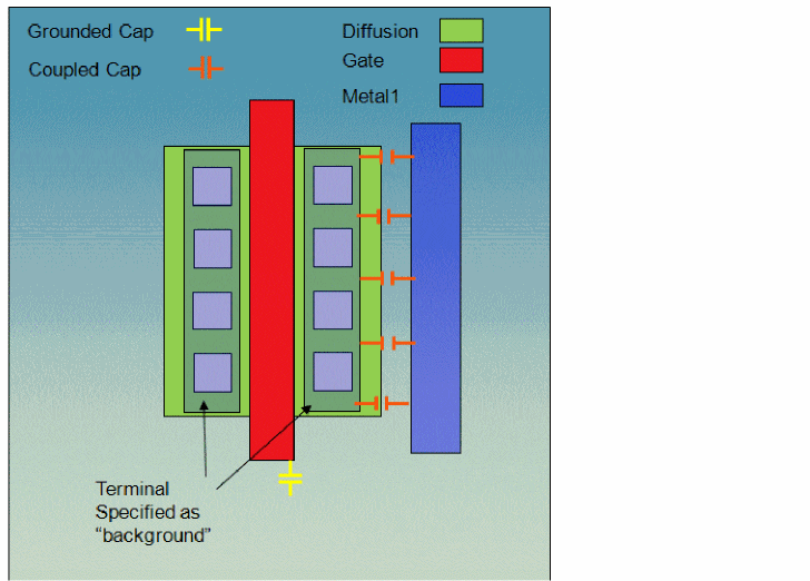
Even though a terminal is defined as background, coupling capacitance is extracted to that net, but no Metal1 to Poly or Metal1 to Metal1 coupling for terminal shapes in devices is extracted.
For more information, see EAD Process Settings – Cell Shape Types and Editing Process Settings.
Preventing Extraction Inside Devices
You can stop Layout EAD from extracting parasitics inside devices using the Primitives & Excluded Cells table on the General tab.
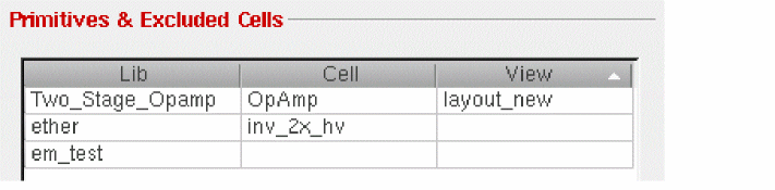
Parasitics are extracted up to and including the terminals of the excluded cells, but no extraction is performed inside the specified devices.
Use this option to exclude devices such as capacitors and resistors, where you do not want to extract resistance and capacitance twice, or for polygonal standard cells or other instances that are not XL compliant.
Device terminals are extracted by default, which means that the resistance on the terminals is computed and all terminal shapes are passed to the extraction engine for capacitance extraction as well (allowing calculation of the coupling capacitance from the terminals to nets outside the Pcell).
See also: extractionPrimitives
Stopping Extraction at the Device Boundary
If, for a given technology, you want to specify that extraction should stop at the boundary of a Pcell or an instance, check the Stop at Device Boundary option in the Extraction tab. By default, EAD extracts parasitics for such shapes. But when this option is switched on, extraction stops at the device boundary, which means that terminals on Pcells and instances are treated as background shapes and are not extracted.
This works in conjunction with the Hierarchy Levels option for instances.
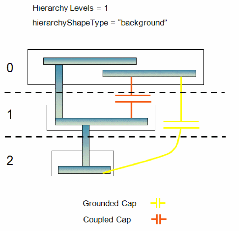
Specifying the Hierarchy Levels and Hierarchy Shape Type
The Hierarchy Levels option on the Extraction tab controls how many levels to chase a net down through the hierarchy and how many levels should be extracted for resistance.
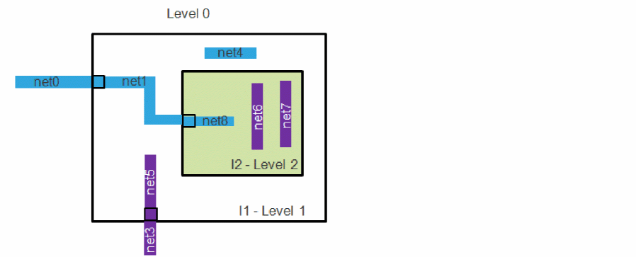
For example, with Hierarchy Levels set to 1 (as shown in the above figure), the following nets are shown in the EAD Browser with R and C extracted:
Decoupled capacitance is extracted to shapes on:
You can also use Hierarchy Levels in conjunction with the hierarchyShapeType environment variable to specify how geometry is treated during extraction. An example is shown below.
Identifying Instances to be Ignored during Extraction
EAD uses the propsUsedToIgnoreObjs variable to look for the properties that identify the pins and instances to be ignored from EM checks. If your layout contains some more instances that are not being ignored by the properties defined by propsUsedToIgnoreObjs, you can apply the eadIgnore property on such instances. This helps in eliminating the irrelevant terminals and shows only relevant parasitic data after extraction.
You can apply the eadIgnore property on a layout cellview to eliminate extraction of all instances of that cellview in your layout. Alternatively, if you unable to edit the cellview, you can select the instances of that cell in your layout and selectively apply the property.
Applying eadIgnore on a Master Layout Cellview
To apply the eadIgnore property on a master layout cellview:
- Open the master layout cellview in the edit mode.
-
Type the following commands in the CIW:
cv = geGetEditCellView()
dbCreateProp(cv "eadIgnore" 'boolean t)
- Save the changes and close the cellview.
After you apply this setting, all instances of this layout are ignored during extraction.
Applying eadIgnore on Specific Instances in the Design Layout
To apply the eadIgnore property on specific instances:
- Open the layout of your design in the edit mode.
- Open the Property Editor assistant.
- Select the instance to which you need to apply this property.
- Right-click in the Property Editor assistant and choose Add Property to <inst-name>.
-
In the Add Property form that is displayed, specify the property name in the Name field as
eadIgnore. -
In the Type field, select the type as
boolean. -
Select the Value check box to set the property value to
t.
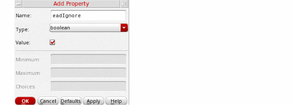
The required property is now set on the instance for which you want to ignore the instance terminals while extracting parasitics.
Modifying EM Analysis for Wide Pins
By default, EAD considers center of the pin as the default current injection point. EAD recalculates the current flowing through the pins, and while doing that considers the resistance on the pin to be zero. That is, the pins are considered to be super conductors.
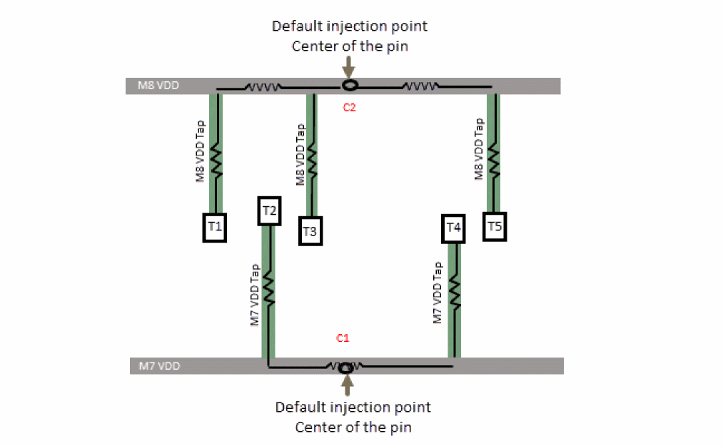
However, for wide pins, you can consider any other current injection point or multiple injection points at specific points that would overlap with the sources of current.
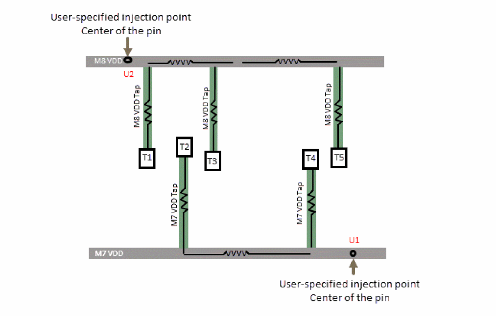
For each injection point, EAD inserts an additional resistor or node on the pin. It then calculates the total current flowing through the pin by considering the values of all resistors on the pin. Therefore, the resistance on pins also impacts the EM violation and IR drop calculations.
You can enable multiple point injection for wide pins in the following ways:
- By editing the layout view to add labels at the injection points
- By providing the location of injection points or nodes in a file
After creating labels or specifying a location file for nodes, run R extraction. New resistances that were added at the nodes are extracted along with other resistance values and their details are displayed on the R tab in the EAD Browser.
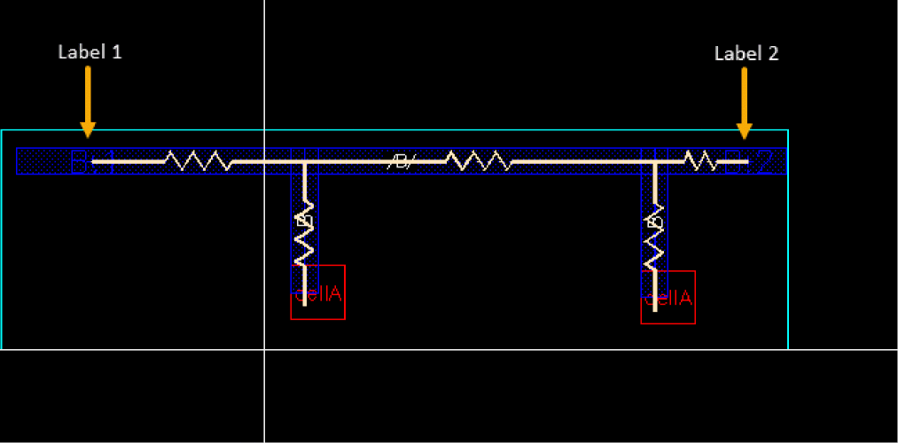
Consider the following example. By default, four resistors are extracted for pin B, as shown below.
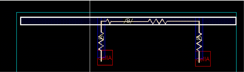
Two labels are added to this pin to specify the current injection points. Running extraction after inserting nodes, returns five resistors, as shown below.
These resistances are considered in EM analysis and reflected in the EM violations reported on the EM tab and IR drop data displayed on the IR Drop tab.
The heat map or IR drop violations for the above example also considers the additional resistance added for the new current injection point.
Editing Layout to Add Labels for Current Injection Point Creation
To add injection points or nodes on a layout:
-
Before launching Virtuoso, set the following two variables in the
.cdsinitfile:- Set insertResNodeLabelPurpose to specify the name of the purpose on which you plan to create labels to be used for the insertion of node injection points.
-
Set stackViaArrayHandling to
"none"to allow the evaluation of EM violations at pins. By default, the pin resistance is considered as zero and EM violations are not calculated for pins.
- Launch Virtuoso and open the layout view.
- Choose Create – Label to open the Create Label form.
-
On the Create Label form,
-
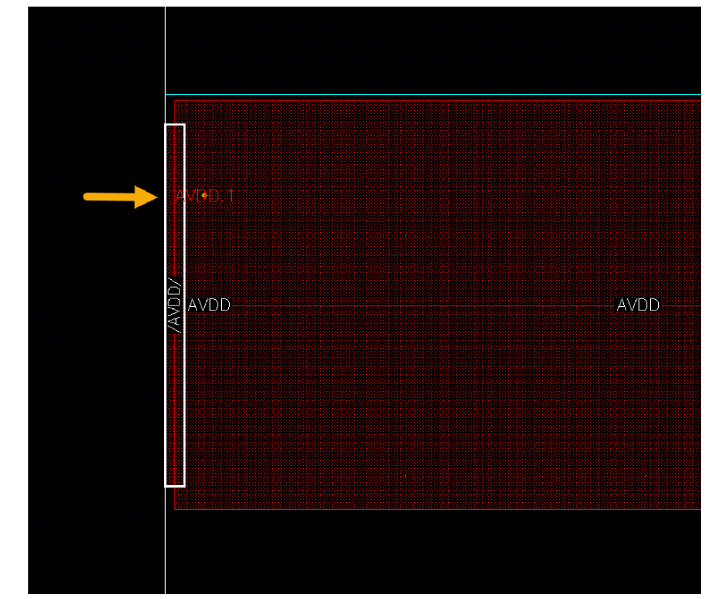
Specify a label pattern in the Label (Pattern) field.
The label pattern must be in the<pin-name>.<positive-integer>format. For example, if you need to create labels for pin A, you can enter the value in the Label (Pattern) field asA.1. - Select the Use same layer as shape, select purpose option and select a purpose name from the drop-down list next to this field.
-
Set the Height label option to a small value, for example,
0.05, so that labels can fit on the pins.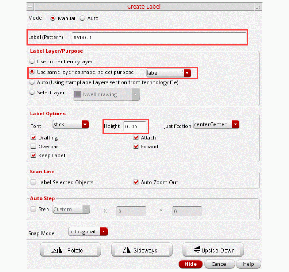
-
Click Hide to close the form and to continue with label creation.
A label is attached to the pointer.
-
Specify a label pattern in the Label (Pattern) field.
- Bring the desired pin in focus and zoom in.
-
Click at the location where you want to add a label on the pin. A label is added with the name mentioned on the Create Label form.
- Create more labels as required.
Adding Current Injection Points Using a File
If you have the current injection point locations available in a text file, you can use that to create injection points on the pins.
The text file should contain the location details in the following format.
#--------------------------------------------
#source_name #loc_x #loc_y #layer_name #P/G
<pinName>.<wholeNumber> <x-coordinate> <y-coordinate> <layerName> <POWER | GROUND>
An example of the text file is given below.
#source_name #loc_x #loc_y #layer_name #P/G
vdd1.0 14.04 3.264 metal2 POWER
vdd1.1 15.12 3.264 metal2 POWER
vdd1.2 6.48 3.264 metal2 POWER
vdd1.3 7.56 3.264 metal2 POWER
To use this file for the insertion of injection points, before launching Virtuoso, set the following environment variables in the .cdsinit file:
- Set insertResNodes to specify the name of the file that provides the location details for nodes to be created for EM analysis of wide pins.
-
Set stackViaArrayHandling to
"none"to allow the evaluation of EM violations at pins. By default, the pin resistance is considered as zero and EM violations are not calculated for pins.
After this, launch Virtuoso and open the layout view for EAD. Run extraction and EM analysis for the net. Layout EAD creates nodes at the specified injection points.
Extracting Parasitics in Layout EAD
Layout EAD extracts parasitics on a net-by-net basis, which makes the tool incremental and able to handle partial layouts.
Before extracting parasitics, you can configure the settings to customize the way EAD extracts parasitics for your layout. For more details, refer to Customizing Extraction of Parasitics.
You can extract parasitics using the Extract Parasitics command in the EAD Browser toolbar. For this, perform the following steps:
-
Choose the setup you require from the Options menu in the EAD Browser toolbar.
The specified setup is loaded. See Managing EAD Setups for more information.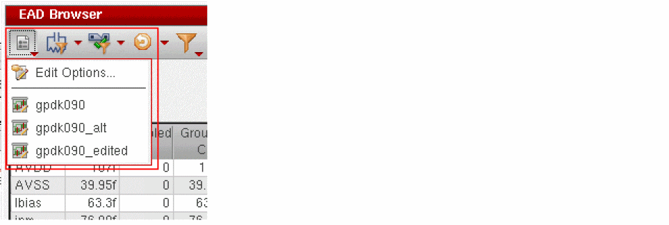 No parasitic extraction or EM checking is run by default; however, any stored parasitic information is retrieved and displayed in the summary pane. EM violations and J/Jmax values are not stored in the OpenAccess database and can only be displayed after you have run the EM check.Any mismatches in the temperature values set for EM checking, extraction, and simulation are reported in a warning dialog.
It is important that you use a consistent temperature throughout your flow; if the temperature used during simulation in ADE Assembler does not match that set for extraction and EM checking in Layout EAD, then your EM analysis is likely to be invalid.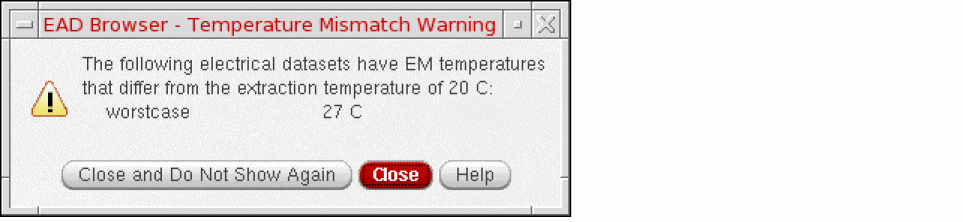
-
Click Extract Parasitics on the toolbar of EAD Browser to extract parasitic information for the design.
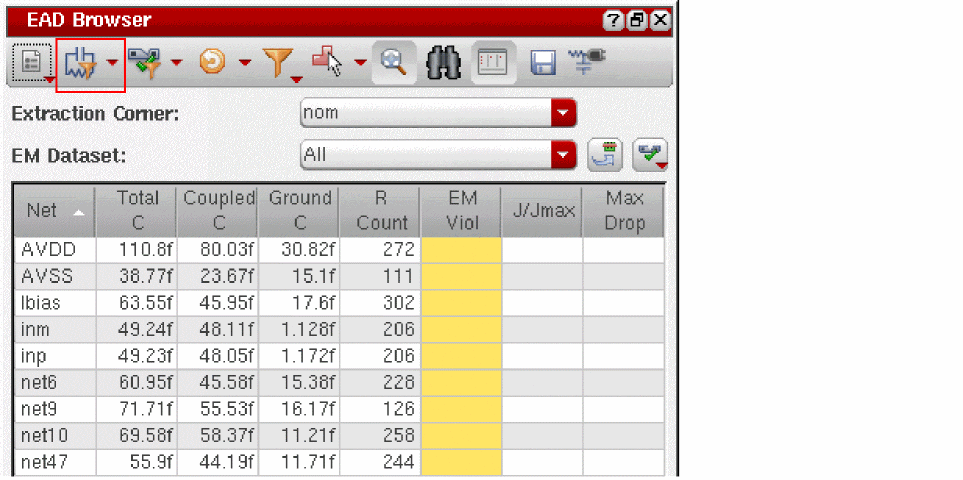 To extract parasitics for one or more selected nets, select their rows in the summary tab, right-click and choose Extract Parasitics from the context-sensitive menu.The summary table is updated to show the parasitics (total, coupled, and grounded capacitance values and total number of resistors) for the listed nets.
- The extraction runs across all the extraction corners specified for a given design. This means that if the same design is open in two different layout windows and the EAD Browser is set up with different extraction corners in each, then extracting or updating in one window will extract and update results for both corners in both windows.
- By default, capacitance values in all tables are displayed in femtoFarad (fF). To vary the units depending on the magnitude of the capacitance values, disable the capacitanceFixedSuffix environment variable.
- By default, the tables show the maximum value of coupling capacitance between nets.
-
By default, only terminals and instance terminals are considered as network terminal objects and a resistance path is computed to them. You can set the extractToPins environment variable to
tso that pins are also considered as network terminal objects and a resistance path is computed to them. -
Violations of any of the supported constraints set in the Constraint Manager assistant are highlighted in red in the appropriate table cells. The supported constraints are:
- Max Resistance
- Max Capacitance
- Max Voltage Drop
- Matched Capacitance
- Max Coupling Capacitance
- High Precision C Extraction
- High Precision R Extraction
For more information on these constraints, see Appendix A, “Default Constraint Types” in the Virtuoso Unified Custom Constraints User Guide. - You can also move the pointer over a net name to see a tooltip indicating whether the parasitic network for the net is complete or incomplete (incomplete networks are also highlighted in yellow).
-
Click one of the table cells to see more detailed information in the appropriate tab in the Detail Pane. For example,
- If you click a capacitance or resistance value, the C or R tab opens with a detailed breakdown of the selected value. See Viewing and Analyzing Parasitics for more information.
- If you select capacitance values for two nets, the Compare tab opens allowing you to compare the information for the nets in question. See Comparing Parasitic Values for Multiple Nets for more information.
-
If you make changes in the layout, you can update the parasitics at any time using the Update Parasitics & EM button or by pressing
Ctrl+u.
You can also right-click in a cell and update the parasitic and EM data, extract parasitics, and run the EM check for a selected net.
For information on updating parasitics automatically while you edit, see Using Automatic Update Mode.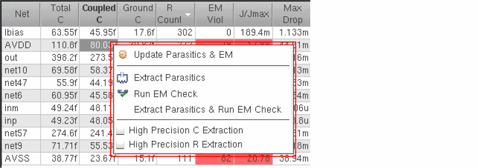 While the extraction process is running, you can use the
Ctrl + Cbindkey to interrupt the process. If you are using this command, ensure that the checkInterrupt environment variable is set tot.
High Precision C and R Extraction
For the critical nets in your design, you can selectively enable high precision C and R solvers. For this, select one or more nets in the Summary pane of the EAD Browser and select the High Precision C Extraction or High Precision R Extraction.
This creates a corresponding
When a port or a node is defined by a pin shape, the high precision R solver uses the geometry of the pin shape to construct a finite dimension port. This helps in correct emulation of the current crowding or spreading at the current inlet or outlet for accurate resistance values. While doing this, the tool follows the rules given below to emulate the pin shape ports:
- If at least one of the edges of a pin shape is aligned with the boundary of layout shape, the current is emulated as flow in or flow out horizontally (in-plane with the layout layer) and perpendicular to the pin shape edge.
- If multiple edges of a pin are aligned with the shape boundary, the longest one is chosen as the port.
- If the pin shape is completely inside the layout shape, the current is emulated as flow in or flow out vertically (perpendicular to the layout layer) and the current flows through the whole area of pin shape.
In the following two cases, EAD marks the resistance network generated for a net by the high precision R solver as complete:
- When all extracted resistors are connected in only one network topology
- When all terminal nodes are included in the network
In all other cases, the resistance network of the net is marked as incomplete and the Net Name cell in the EAD Browser is highlighted in yellow.
Customizing High precision R and C Extraction
Depending on your requirements, you can customize high precision R and C extraction by setting the fields in the High Precision C Solver and High Precision R Solver sections on the
-
Each capacitance value, C (estimate), reported by the High Precision C solver is a statistical average with an associated standard error. This standard error is determined by the convergence target or goal set by the convergenceCThreshold environment variable or the Default Convergence Target field on the EAD Options form. The convergence target relates the statistical average to the actual capacitance value, C (actual).
For example, if the reported C (estimate) for a given net is10.0ffwith a convergence target of4.0%, then the standard error is4.0%of10.0ff, which is0.4ff. It can be said with 99.7% confidence that the difference between C (actual) and C (estimate) is not more than 3 times of the standard error, which is1.2ff. This also means that the error in C (estimate) is not more than 3 times of the standard error.
The example in the table given below shows how different values of convergence target change the accuracy of the reported C (estimate) of 10.0ff. With decreasing convergence targets, the maximum error in the C (estimate) value is reduced. That means, the reported C (estimate) becomes more accurate, but at an increased run time. If the convergence target it reduced to half, the run time increases four times (by 4x).Convergence Target Standard Error Max Error in C (estimate) confidence Run time (seconds) -
The default mesh density value used by the high precision R solver is
1.0. If required, you can change this default by setting the resistanceMeshDensity environment variable or the Default Mesh Density field on the EAD Options form. A larger mesh density value creates a denser mesh, which also takes a longer time to run R extraction.You can use separate layer-wise mesh density values provided in a source text file by setting the resistanceMeshDensityFileName environment variable. - You can use the resistanceMesherTimeOut environment variable to specify a threshold time to be compared with the estimated time to perform high precision R extraction for a net. If the estimated time is longer than the threshold time specified by this variable, high precision R extraction is stopped. A warning message is displayed and the remaining extraction for that net is not done.
-
While performing high precision R extraction for a net, Layout EAD can save the mesh data, current density and voltage drop data in temporary binary files. These details can be later overlaid on the layout.
The file in which the mesh data is saved is specified by the resistanceMeshFileName environment variable. Similarly, the file in which the current density and voltage drop data is saved is specified by the resistanceFieldFileName environment variable. If required, you can set the values of these variables to a writable file location.
Also see: Running EM Checks with High Precision R and C Extraction - The width values displayed in the W column of the Resistances table are calculated by the mesh solver. They may not match the width drawn on the layout.
-
By default, high precision R extraction performs via clustering and considers the rules defined on the Vias tab of the EAD Process Settings form. To disabled via clustering in high precision R extraction, set the hprDisableViaClustering environment variable to
t. - You can set the useNumberOfGPU environment variable to enable Graphical Processing Unit (GPU) computing for high precision C extraction and to specify the number of GPUs to be used.
-
By default, high precision C extraction does not include vias in the modeling for capacitance extraction. You can include vias by setting the modelViaCapacitanceEffect environment variable to
t, or by selecting the Via Effects check box on the Extraction tab of the Layout EAD Options form. -
You can include the non-gate forming poly shapes in the modeling for poly to diffusion capacitance extraction by setting the modelNonGateFormingPolyCap environment variable to
t. -
By default, high precision C extraction models the actual metal fills that physically exist in the design. The fill metal modeling method can be selected from the Metal Fill Modeling Method drop-down list on Extraction tab of the EAD Option form.
By setting the hpcMetalFillDefFileName environment variable, you can enable the virtual metal fill modeling capability to study the impact of metal fills on capacitance values at an early design stage, even if the actual metal fills have not been added to the design database. When virtual metal fill modeling is enabled, high precision C extraction uses the available modeling information to add virtual metal fills into the geometry model for capacitance extraction. These metal fills are added only virtually and the flow does not change the design database, but the extraction process obtains the capacitance values by assuming that metal fills exist there physically.
If the design database contains actual metal fill shapes, they will be modeled along with the virtual metal fills as an effective way of incremental extraction. If there is an overlap of the actual and virtual metal fill, the actual metal fill will be considered for modeling, and the virtual fill will be ignored.
While setting the hpcMetalFillDefFileName environment variable, you can provide the virtual metal fill modeling information in the following ways:-
In a model definition file in the following ASCII format:
where,
- num_of_blocks is an integer value that defines the number of custom virtual metal fill definition blocks given in this definition file;

- layer_name is a string value that defines the layer name in the technology file (ICT file)

- num_of_vertices is an integer value that defines the number of vertices used to define unit polygon metal fill shape. It was followed by num_of_vertices pair of floating point number to define the polygon, each represents X and Y coordinates of one vertex. These vertices can be listed either in clockwise or counter-clockwise order.

- min_net_fill_spacing is a float value that defines the minimum spacing between an edge of a net and a parallel edge of a metal fill shape;

- min_X_fill_spacing is a float value that defines the minimum spacing between any two horizontal edges of neighboring fill metal shapes

- min_Y_fill_spacing is a float value that defines the minimum spacing between any two vertical edges of neighboring fill metal shapes
A sample of the metal fill definition file is given below.2 M1 4 0.0 0.0 0.12 0.0 0.12 0.12 0.0 0.12 0.3 0.3 0.3 M2 4 0.0 0.0 0.12 0.0 0.12 0.12 0.0 0.12 0.3 0.3 0.3
In this case, set the hpcMetalFillDefFileName environment variable to the path of the model definition file. EAD reads the information from this file to create virtual metal fills in the design. -
In the ICT file. If you want to use the virtual fill definition only from the ICT file, set the hpcMetalFillDefFileName environment variable to the name of a text file that contain only one line
"0", which indicates that no custom virtual fill definition should be used.
For details about the format of virtual metal fill definition in ICT file, refer to themetal_fillcommand in the Quantus QRC Techgen Reference Manual. - In both, the ICT file and the virtual metal fill definition file. In this case, you can set the hpcMetalFillDefFileName environment variable to the path of the text file that contains the modeling parameter definitions. The modeling parameters are read from both the sources. However, if the parameters for a particular layer are given in both the sources, the parameters given in the definition file have higher preference.
-
In a model definition file in the following ASCII format:
-
If an ICT file contains via bias and spacing dependent contact bias, or VEEs (Via Edge Enlargements), high precision C extraction includes those in the capacitance models for extraction.
For via bias, the ICT file must include thevia_top_enlargementandvia_bottom_enlargementparameters in via definitions, as shown below.via "ViA1" { top_layer METAL_2 bottom_layer METAL_1 contact_resistance 7.9 min_top_encl 0.010 min_bot_encl 0.011 min_width 0.08 min_spacing 0.08 via_top_enlargement 0.1 via_bottom_enlargement 0.1 }
For VEEs, the ICT file must include thevia_edge_enlargementparameter in via definitions, as, shown below.via_edge_enlargement vee_coco_spacings S1 S2 ... Sn vee_poco_spacings S1 S2 ... Sm vee_adjustments A11 A12 ... A1n A21 A22 ... A2n ... Am1 Am2 ... Amn
In addition, a sub via mapping file in ASCII format that provides the mapping for layout via layer name to its corresponding tech file sub via layer name is also required. The file should be named assubvia_layer_mapping.txtand saved in the same directory that containseadTechFile.
An example of the sub via mapping file is shown below.------------------
CO DEMOS_odCont
PO NMOS_odCont
------------------
In this example, CO is the layout layer name and DEMOS_odCont is the mapping sub via layer name.
While extracting capacitance for a layer in the layout, EAD uses the VEE table defined for the sub via mapped to it. -
By default, high precision capacitance extraction does not include modeling of spacing-dependent dielectric constant on metal interconnect layers. You can set the following SHELL environment variable before starting Virtuoso to enable variable dielectric effect:
setenv HPC_ENABLE_VARIABLE_EPSILON 1
finFET Support in High-Precision C Extraction
If your design contains multi-gate finFET devices, you can enable finFET modeling in high-precision C extraction by doing the following:
-
Specify a fin width value using the finWidth environment variable and a fin spacing value using the finSpacing environment variable. These values should be greater than
0.0. The tool uses these two values to enable finFET modeling and to generate fin geometries. -
Set the modelViaCapacitanceEffect environment variable to
t. -
Set the modelNonGateFormingPolyCap environment variable to
t.
If the ICT file contains thefin_widthandfin_spacingkeywords for the active layer, the values defined by the finWidth and finSpacing variables will be overridden by the values of these two keywords. However, it is still required to set the values of these two variables to a non-zero value to enabled finFET modeling.
iQuantus FS C Extraction (Advanced Nodes Layout EAD Only)
For sign-off level accuracy in extraction results, you can use iQuantus Field Solver (iQuantus FS) as the capacitance extraction engine. The C parasitic data extraction run by iQuantus FS is accurate.
Before using iQuantus FS engine for extraction, ensure that the following requirements are met:
- The following environment variables are set:
-
The Engine field on the Extraction tab of the EAD Options form is set to
quantusFS.
Follow these steps to use iQuantus FS for C extraction:
-
In the High Precision C Solver section on the Extraction tab of the EAD Options form, from the Engine drop-down list, select
quantusFS. - To run extraction for all nets, click Extract Parasitics for All Nets from the EAD Browser toolbar.
- To run extraction for the selected nets, do the following:
Viewing and Analyzing Parasitics
This section describes how to use the EAD Browser to view and analyze the capacitance and resistance information for your design and explains what information is available for each.
- Click a capacitance value in the summary pane to open the C tab in the detail pane.
-
Use the toolbar buttons to toggle capacitance information by net, by layer, or by node.
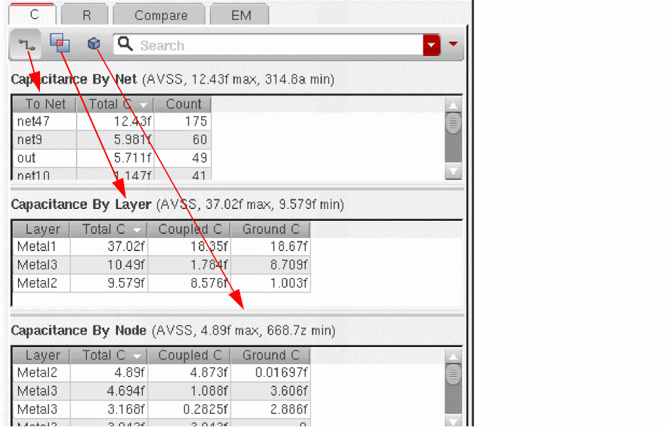
-
Click a resistance value in the summary pane to open the R tab and see the terminal-to-terminal resistance paths for the net in question, including the resistance value, resistor count, and from/to terminal names.If you have set the resistanceMeshFileName environment variable, the mesh data is saved while performing high precision R extraction for any net. You can later overlay that data on the net in the layout canvas. For more information, see Viewing Mesh for Selected Nets.
-
Move the pointer over a Total R violation in the summary pane to see a tooltip detailing the violating resistance path, which is also highlighted in the R tab.If all the violations are not displayed in the tooltip, you can increase the size of tooltip by using the maxTooltipLength environment variable.
-
Click a row in the R table to highlight the corresponding resistance path in the layout view.
If there is only one resistance path for a net, the resistance path is selected by default after you extract parasitics for that net. Only the resistors available on the resistance path are displayed in the Resistances table.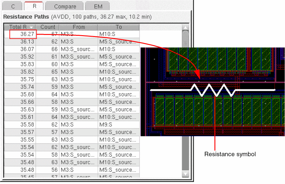
If you deselect the resistance path, all resistors that overlap with the net are displayed in the Resistances table.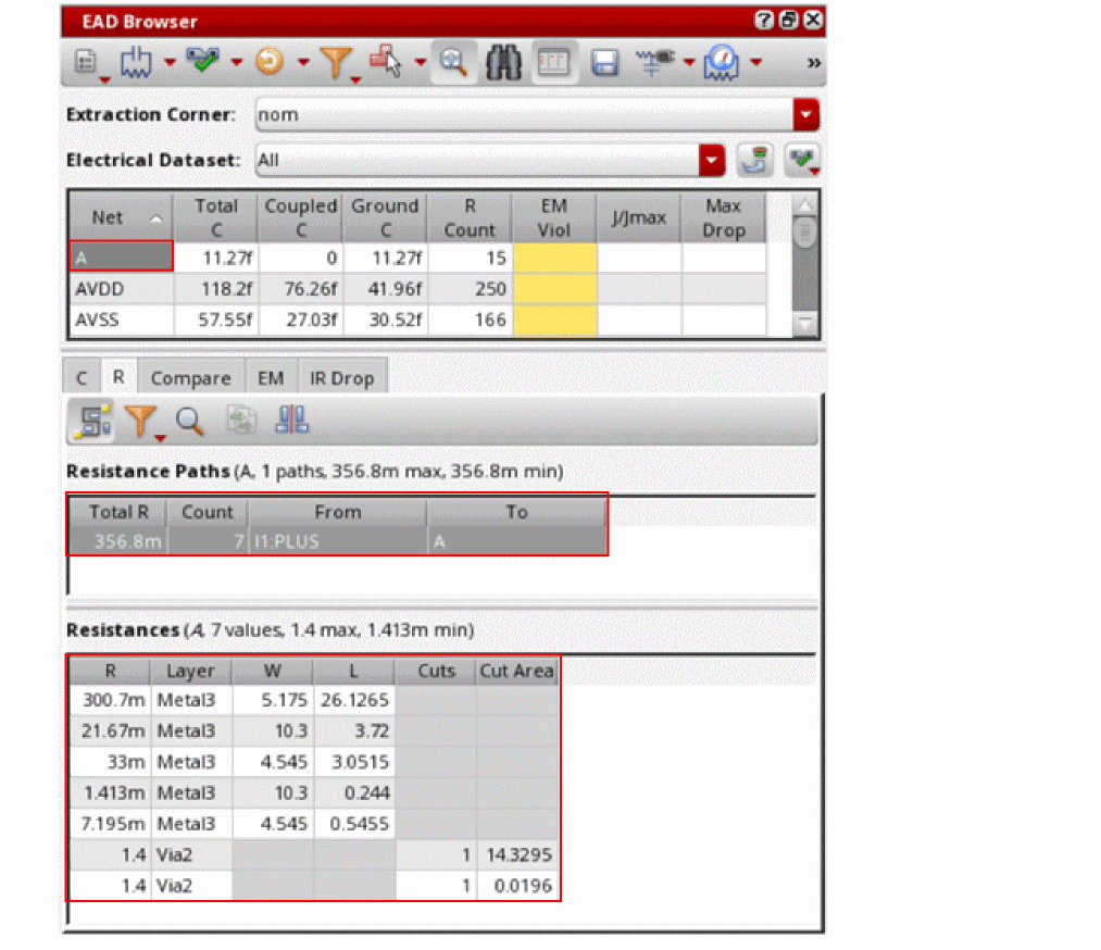
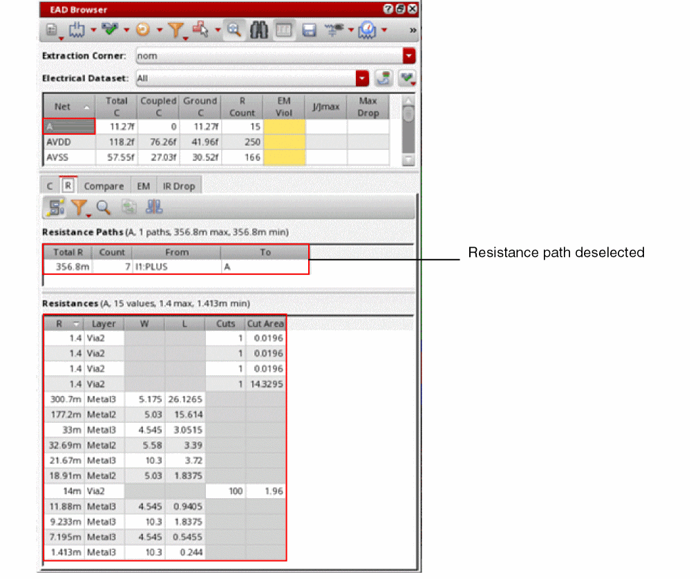 By default, Layout EAD uses a resistor symbol to highlight a resistance path on a net. You can set the resistanceDisplay environment variable to
"halo"to use a halo instead, as shown below.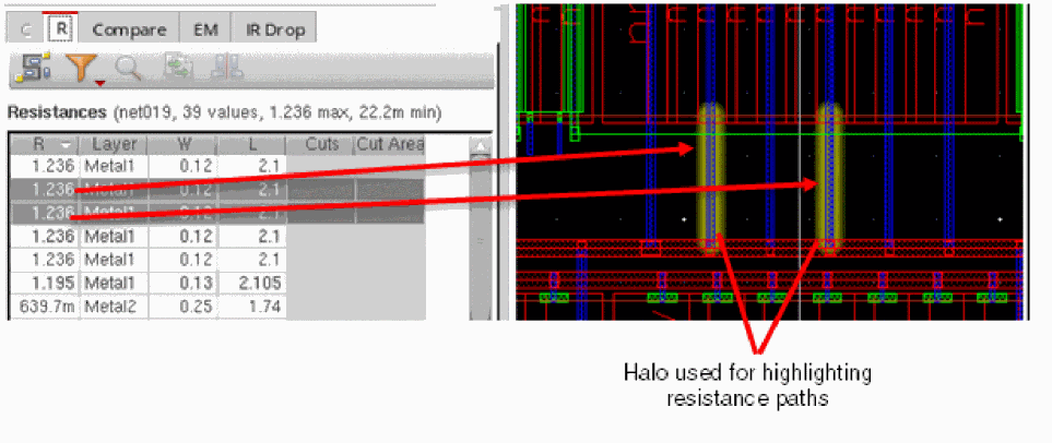
Viewing Mesh for Selected Nets
If you have set the resistanceMeshFileName environment variable, while performing high precision R extraction for selected nets, mesh data is saved in the specified binary file. In addition, the Highlight mesh (![]() ) icon also appears on the toolbar of the R table. The names of nets for which high precision extraction was performed also appear as bold, as shown below.
) icon also appears on the toolbar of the R table. The names of nets for which high precision extraction was performed also appear as bold, as shown below.
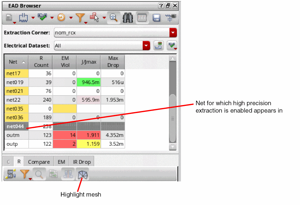
To overlay the saved mesh data on a net in the layout canvas, do the following:
- Click the resistance value for that net in the summary pane to open the R tab in the detail pane.
-
Click Highlight mesh.
A mesh is displayed on the selected net in the layout. -
Zoom in to a large level to view the mesh details clearly.
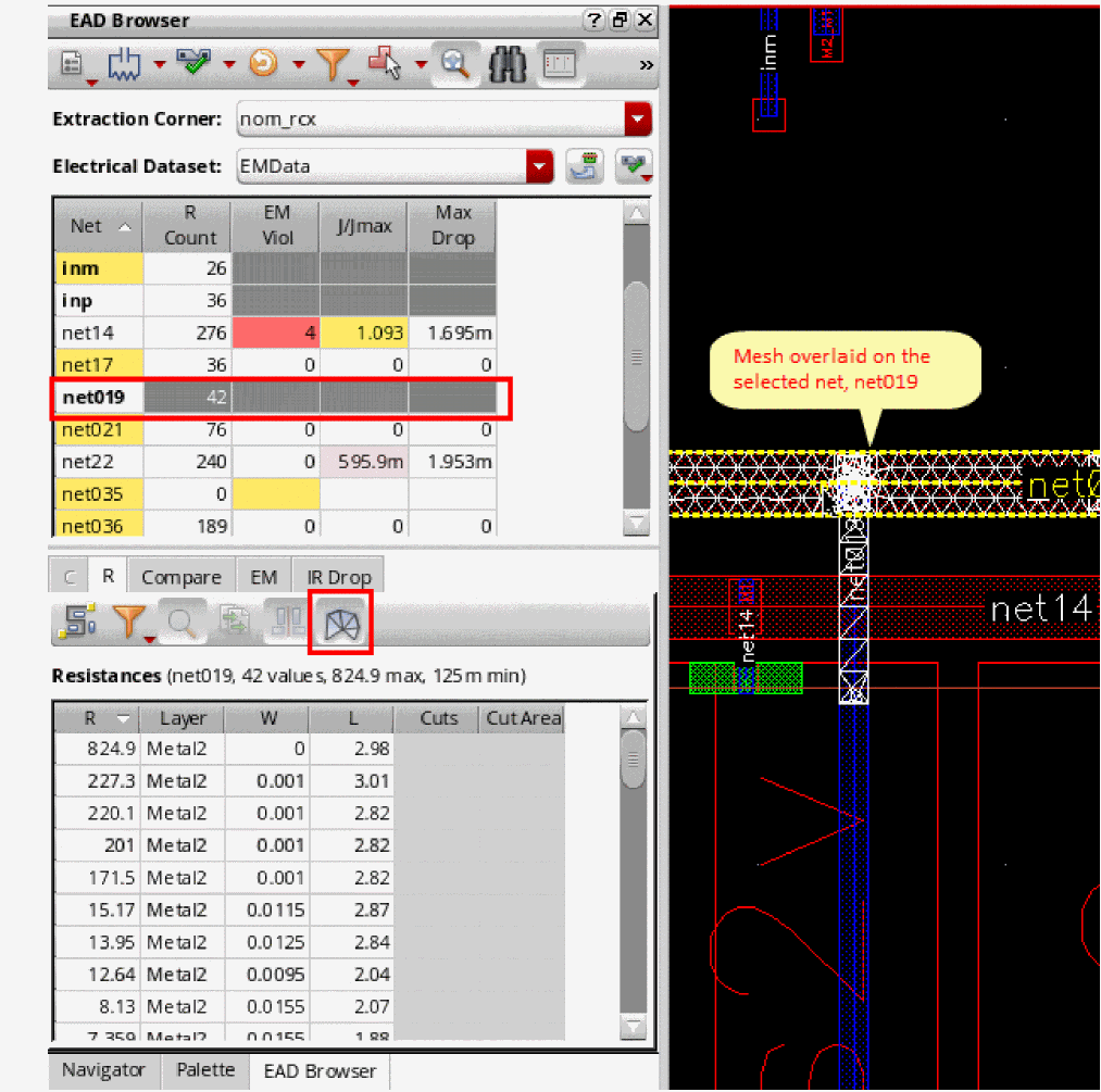
- You can reset the layer filter to view the mesh on specific layers.
Important Points to Note
- The mesh data extracted during high precision extraction is saved in the binary files specified using the resistanceMeshFileName environment variable. After the analysis is complete, you can choose to delete the saved files.
- The Highlight mesh button on the toolbar of R tab is enabled only for those nets for which high precision extraction has been done and mesh data is available.
-
Consider a case when you have displayed the mesh data for a net on the layout canvas.If you open any other layout cellview that contains a net with the same name for which mesh data is available, the Highlight mesh (
 ) button remains enabled because the binary file is available in the current working directory. However, when you click Highlight mesh, the tool detects that the mesh data file is not for the current cellview, and deletes it. To display mesh data for the net in the current layout cellview, you need to again extract the parasitics using high precision extraction.
Comparing Parasitic Values for Multiple Nets
If you select two or more values in the summary pane, the Compare tab opens comparing values for the selected nets. This can be useful if, for example, you have a pair of symmetric nets that need to be balanced in terms of parasitics. You can select the nets in the layout canvas and compare the coupled and grounded capacitances of the nets and the amount of coupling to other nets in the design.
-
Select two or more values in the summary table.
The Compare tab opens showing the maximum difference and % error between the parasitic values on the selected nets. -
Use the Reference Net drop-down to choose which of the selected nets is the reference net for the percentage difference calculation.
The default is Auto, which means that the net with the smallest value is used as the reference for the difference calculation. You can change this as required, for example, when comparing the lengths of bus bits that are intended to be matched.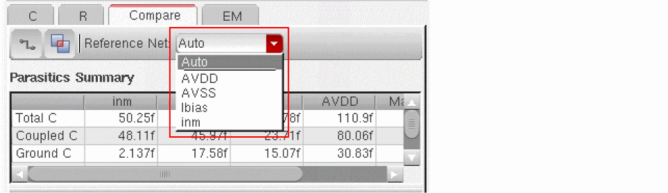
- Use the two toggle buttons on the toolbar to show and hide tables comparing
-
Click an entry in the Coupling Capacitance by Net table to highlight the net in the layout canvas.
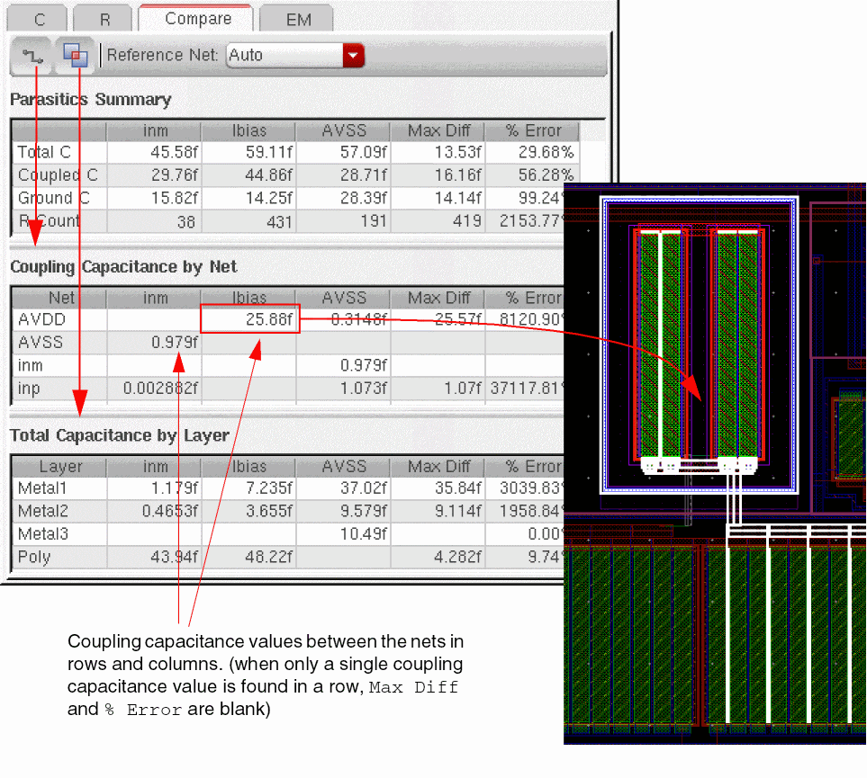
Using Automatic Update Mode
By default, EAD does not extract dynamically as you update the design, but tracks the changes you make and highlights in red nets that need to be extracted. You then run the extraction by clicking the Update Parasitics & EM button in the EAD Browser toolbar (or by pressing Ctrl+u).
You can use Automatic Update Mode to extract parasitic information while you are editing your design in the layout canvas. Any net that has previously been extracted is automatically updated in this mode, even if the parasitics have been deleted due to some other user action.
To update the parasitic information dynamically while you are editing the design,
-
Choose Automatic Update Mode from the Update Parasitics & EM menu.
Now when you edit your design by, for example, routing a net in the canvas, you will see the values in the EAD Browser updating as you work.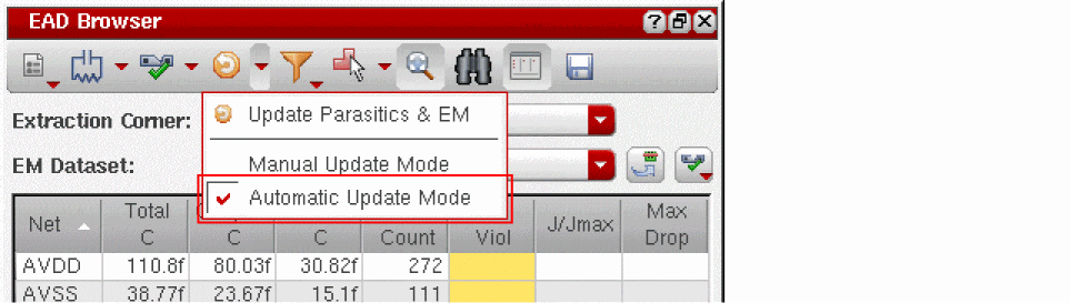
This lets you see immediately the effect that your interactive changes are having on the parasitics for the design.
Distributed Computation of Extraction Process
For large designs, you can distribute extraction on groups of nets to multiple batch jobs running on computer farms or dedicated servers.
Layout EAD provides the following SKILL functions to run and manage distributed jobs for extraction:
Depending on your extraction requirements and the available resources, you can submit extraction jobs in any of the following ways:
- Automatic submission of jobs for all nets to an LSF farm
- Automatic submission of jobs for all nets to dedicated servers
- Customized distributed computation of net groups using different job policies
Automatic submission of jobs for all nets to an LSF farm
Preferred Scenario: Use this approach to submit jobs for extraction on all nets in your design to an LSF farm.
-
Specify the following settings to enable the tool to automatically submit jobs:
- Using the ead_dp_net_group_number variable, specify the number of net groups into which all the nets from the design are to be distributed equally.
- Using the ead_dp_batch_command variable, specify the batch command to distribute a job to an LSF farm.
- Using the ead_dp_batch_command_option variable, specify the option string used by the batch command defined by the ead_dp_batch_command variable.
-
Start the job submission using the eadJobSubmit SKILL function.As configuration information is generated automatically by the tool in this mode, specify the second argument of the eadJobSubmit SKILL function asLayout EAD divides all the nets from the design into the specified number of net groups and distributes the extraction jobs using the given batch command and its options. The number of LSF jobs submitted is equal to the number of net groups.
"NULL".
After job submission, you can use eadJobStatus to check the status of running jobs. When eadJobStatus command returnst, which means all jobs have been successfully completed, you can run eadJobClose to collect the extraction results. The results from all the jobs will be combined into one OA database and displayed in the summary table of the EAD Browser.
Open a layout view in Virtuoso Layout EAD and set the following variables in the CIW:
ead_dp_net_group_number = 5
ead_dp_batch_command = "/grid/sfi/farm/bin/bsub"
ead_dp_batch_command_option = "-W 3:00 -q lnx64 -R \"OSREL==EE50 || OSREL==EE60 span[hosts=1] rusage[mem=8000]\" -P IC:6.1.6:RD:QUAL"
Run the following command in the CIW:
eadJobSubmit( hiGetCurrentWindow() "NULL" )
Layout EAD automatically divides all nets into five groups and submits the jobs using the given command and options. After that, run the following command to check job status:
eadJobStatus( hiGetCurrentWindow() "NULL" )
When all the jobs are complete, run the following command to collect the results from all jobs:
eadJobClose( hiGetCurrentWindow() "NULL" )
Automatic submission of jobs for all nets to dedicated servers
Preferred Scenario: Use this approach to submit jobs for extraction on all nets in your design to a set of dedicated servers in your setup.
-
Specify the following settings to enable the tool to automatically submit jobs:
-
Using the
ead_dp_server_namesvariable, specify the list of available servers on which the distributed jobs can run. -
Using the
ead_dp_batch_commandvariable, specify the batch command to distribute jobs to dedicated servers. -
Using the
ead_dp_batch_command_optionvariable, specify the option string used by the batch command defined by theead_dp_batch_commandvariable.
-
Using the
-
Start the job submission using the eadJobSubmit SKILL function.Note: As configuration information is generated automatically by the tool in this mode, specify the second argument of eadJobSubmit asLayout EAD divides all nets from the design into a set of net groups where the number of groups is equal to the number of servers specified by the
"NULL".ead_dp_server_namesvariable and distributes the extraction jobs using the given batch command and its options.
After job submission, you then can use eadJobStatus to check the status of running jobs. When eadJobStatus returnst, which means all jobs have been successful completed, you can run eadJobClose to collect the extraction results. The results from all the jobs will be combined into one OA database and displayed in the summary table of the EAD Browser.
Open a layout view in Virtuoso Layout EAD and set the following variables in the CIW:
ead_dp_server_names = '("server1" "server2" "server3")
ead_dp_batch_command = "/usr/bin/rsh"
ead_dp_batch_command_option = "-l username"
Run the following command in the CIW:
eadJobSubmit(hiGetCurrentWindow() "NULL")
Layout EAD automatically divides all nets into three groups and submits the jobs using the given command, and options to servers server1, server2, and server3.
Run the following command in the CIW to check job status:
eadJobStatus(hiGetCurrentWindow() "NULL")
When all jobs finish and the above command returns t, run the following command to collect results from all jobs:
eadJobClose(hiGetCurrentWindow() "NULL")
Customized distributed computation of net groups using different job policies
Preferred Scenario: Use this approach when you want to submit the extraction jobs for a particular net group to a specific distributed job. In this case, you can have multiple customized job policies and specify which policy is to be used for each net group. You can specify these details in a job configuration file that is provided to the eadJobSubmit SKILL function.
-
Create a job configuration file in the ASCII format that contains the layout cellview details of the layout cellview, and the names of files that define the net groups and job policies to be used for each net group.
The expected format of a job configuration file is given below.<job_policy_definition_file_name> <net_group_definition_file_name> <oa_lib_top_level_path> <oa_library_name> <oa_cell_name> <oa_view_name>NULL //reserved for future use -
A job policy definition file in ASCII format that contains one default job policy and some custom job policies. The given number of custom policies is also specified in this file.
The expected format of a job policy definition file is given below.
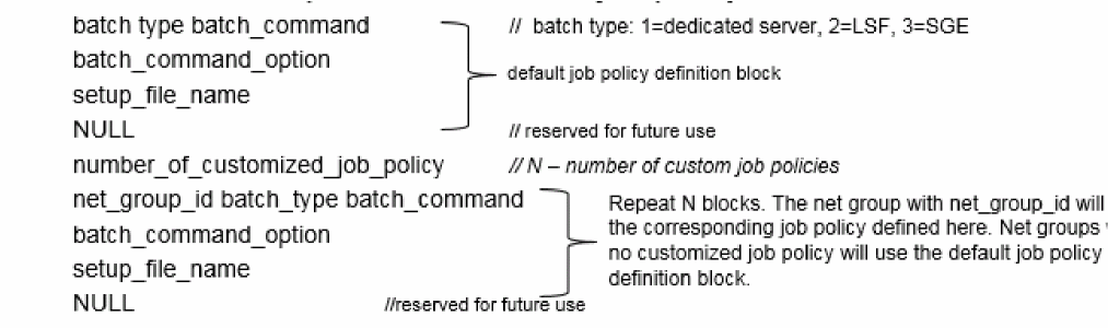
-
A net group definition file in ASCII format that specifies the number of net groups, and the net details for each group.
The expected format of a job net group definition file is given below.
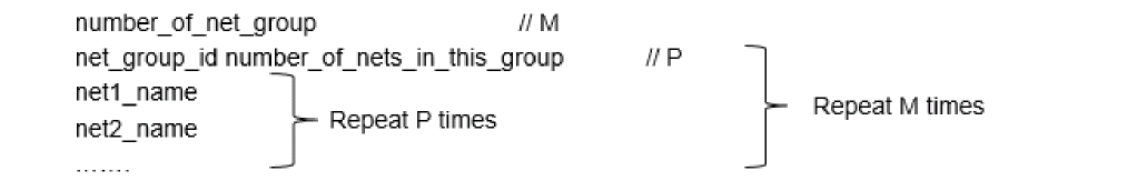
-
Start the job submission using the eadJobSubmit SKILL function.Specify the name of the configuration file created in step 1 in the second argument of the eadJobSubmit SKILL function.Layout EAD reads the net group details from the net group definition file and submits the job for each net group as per the job policy definition attached to it.
Following are the examples of the three ASCII files.
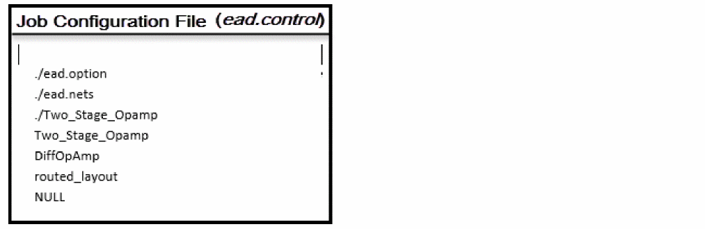
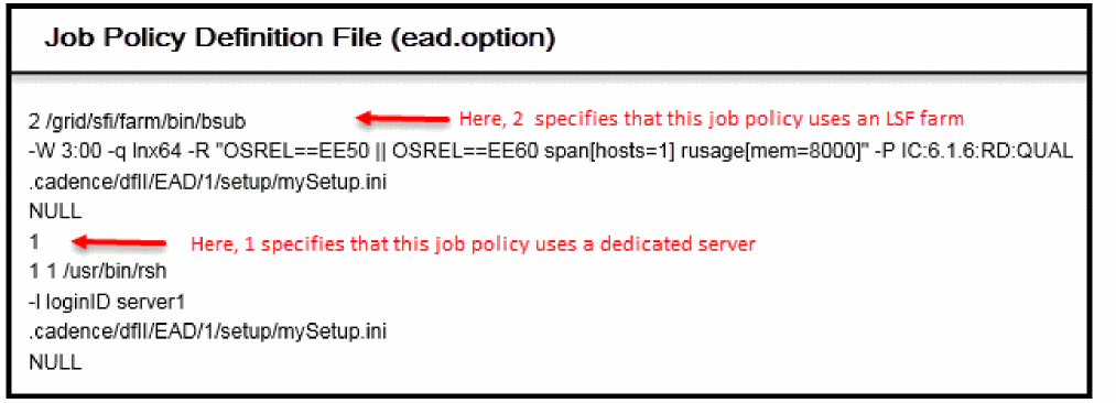
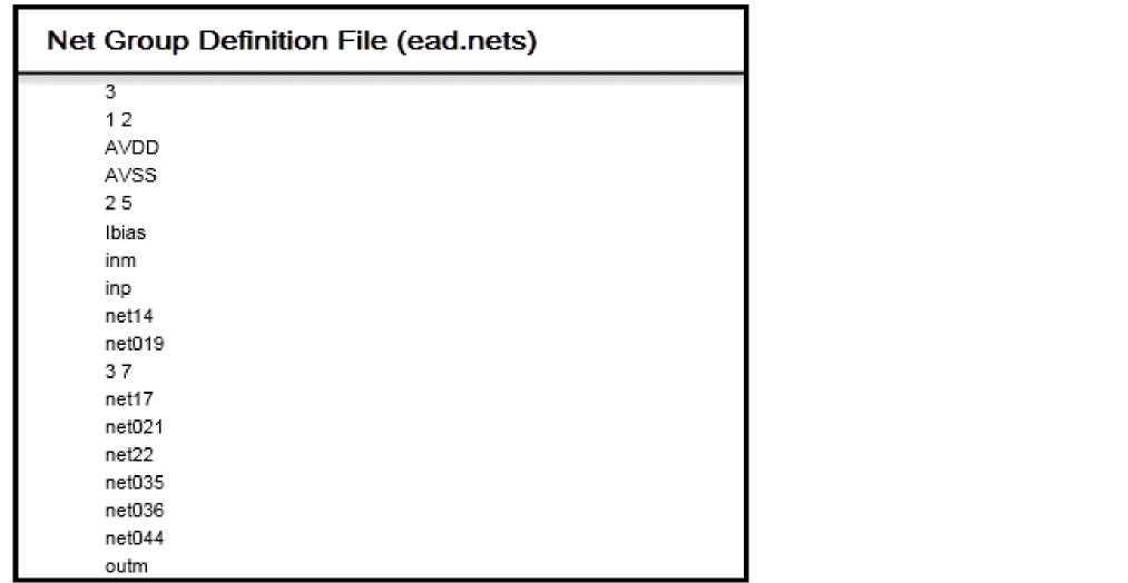
Run the following commands in CIW to submit jobs, check job status, and collect job results:
eadJobSubmit( hiGetCurrentWindow() "ead.control" )
eadJobStatus( hiGetCurrentWindow() "ead.control" )
eadJobClose( hiGetCurrentWindow() "ead.control" )
As specified in the job policy definition, the tool runs extraction on net AVDD and AVSS on the dedicated server server1, whereas each one of the other two net groups is run as a separate job on the LSF farms.
Working with Job Policies
This section describes how to set up a job policy and define the methods of how distributed processing jobs are submitted to local or remote hosts. In EAD, you can use these jobs to extract parasitics and to run EM analysis.
Setting Up a Job Policy
Follow these steps to set up a job policy:
-
On the Environment tab of the EAD Options form or on the EAD Net Options form, click the Edit job policies icon (
 ) to open the EAD Job Policy Editor form.
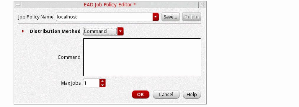
-
In the Job Policy Name field, specify a name for the job policy.If no job policy has been set up earlier, the Job Policy Name field displaysWhen using a job policy other than
localhostas the default job policy name, which can be specified by setting the defaultJobPolicy environment variable.localhost, ensure that Max Jobs field is set to a value less then or equal to the number of available licenses. - From the Distribution Method drop-down list, choose one of the following methods:
-
Depending upon the Distribution Method you selected, specify the fields described as follows:
Distribution Method Fields Description bsubcommand to submit a job for batched execution by a distributed load-sharing batch system -
Click Save to save the changes. The EAD Save Job Policy form opens, as shown in the following figure:
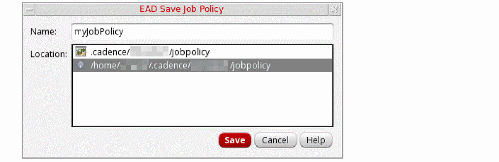
- The Name field displays the name of the job policy you specified in the EAD Job Policy Editor form.
- From the Location list, select the directory where you want to save the job policy. You can save the job policy in one of the following directories:
-
Click Save to save the changes.
You can now extract parasitics and run EM analysis for the nets with the job policy you defined. See the Using Distributed Processing Jobs section for more information.
Editing a Job Policy
Follow these steps to edit a job policy:
- On the EAD Job Policy Editor form, from the Job Policy Name drop-down list, select the job policy that you want to edit.
-
From the Distribution Method drop-down list, select a distribution method.
-
Depending upon the Distribution Method you selected, update other fields, as required.
See the Setting Up a Job Policy section for the description of the fields in the EAD Job Policy Editor form. - Click Save. The EAD Save Job Policy form opens.
- From the Location list, select the directory where you want to save the updated job policy.
- Click OK.
Deleting a Job Policy
-
In the EAD Job Policy Editor form, from the Job Policy Name drop-down list, select the job policy you want to delete, and then click Delete.
The selected job policy is deleted.
Using Distributed Processing Jobs
In EAD, you can use the distributed processing jobs to extract parasitics and to run EM analysis for all the nets or for the selected nets.
To use distributed processing jobs for all the nets, do the following:
- Click the Environment tab on the EAD Options form.
- In the Job Policy Setup section, from the Default Job Policy drop-down list, select a job policy you have already defined. If you want to define a new job policy, click Edit job policies. See the Setting Up a Job Policy section for more information.
- Click OK to close the form.
-
Click one of the following commands on the EAD Browser toolbar:
- Extract Parasitics For All Nets: To use the jobs for extracting parasitics for all nets.
- Run EM Check On All Nets: To use the jobs for running EM checks on all nets.
- Extract Parasitics & Run EM Check: To use the jobs for both, extracting parasitics and running EM checks.
The jobs are submitted according to the methods defined in the selected job policy and results are updated in the table.
To use the distributed processing jobs for the selected nets, do the following:
- In the Summary pane of the EAD Browser, select the nets for which you want to extract parasitics or run EM analysis.
-
Right-click the selected nets and then choose Net Options. The EAD Net Options form opens, as shown in the following figure:

-
From the Job Policy drop-down list, select the job policy that you want to use.You can also click the Edit job policies icon (
 ) to open the EAD Job Policy Editor form, where you can update the existing job policies or define a new job policy. See the Setting Up a Job Policy section for more information.
 - Click OK to save the changes.
-
In the Summary pane of the EAD Browser, right-click the selected nets and then choose one of the following options from the context menu:
- Extract Parasitics: To use the jobs only for extracting parasitics.
- Extract Parasitics With Policy: To select another job policy to extract parasitics for the selected nets.
- Run EM Check: To use the jobs only for running EM analysis.
- Extract Parasitics & Run EM Check: To use the jobs for both, extracting parasitics and running EM analysis.
The jobs are submitted according to the methods defined in the selected job policy and results are updated in the table.
Important point to note:
- All the four engines are supported for distributing processing jobs.
- If you make any changes in the design after submitting the distributed processing jobs, the extraction or EM results may be inconsistent.
Stopping and Resubmitting a Job
Status of the submitted jobs is shown below the EAD Browser toolbar. For example, the following figure shows that a submitted job is currently running:
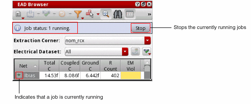
You can click Stop to stop the currently running jobs. Alternatively, you can right-click the selected nets, and then choose Stop Job from the context menu to stop the jobs. The jobs that have not been finished are stopped and the following status is displayed:
A ‘cross’ icon (![]() ) is displayed next to the nets for which the jobs have failed or stopped. You can click Resubmit to submit the unfinished jobs again. After all the jobs are executed successfully, the extraction results are updated in the Detail pane.
) is displayed next to the nets for which the jobs have failed or stopped. You can click Resubmit to submit the unfinished jobs again. After all the jobs are executed successfully, the extraction results are updated in the Detail pane.
Extracting Parasitics With a Policy
You can also extract parasitics for the selected nets using the Extract Parasitics With Policy command:
- In the Summary pane of the EAD Browser, select a net. To select multiple nets, hold down the Ctrl key while you click the other nets you want to select.
-
Right-click the selected nets to open the context-sensitive menu, and then point to Extract Parasitics With Policy. A list of job policies is displayed, as shown in the following figure:
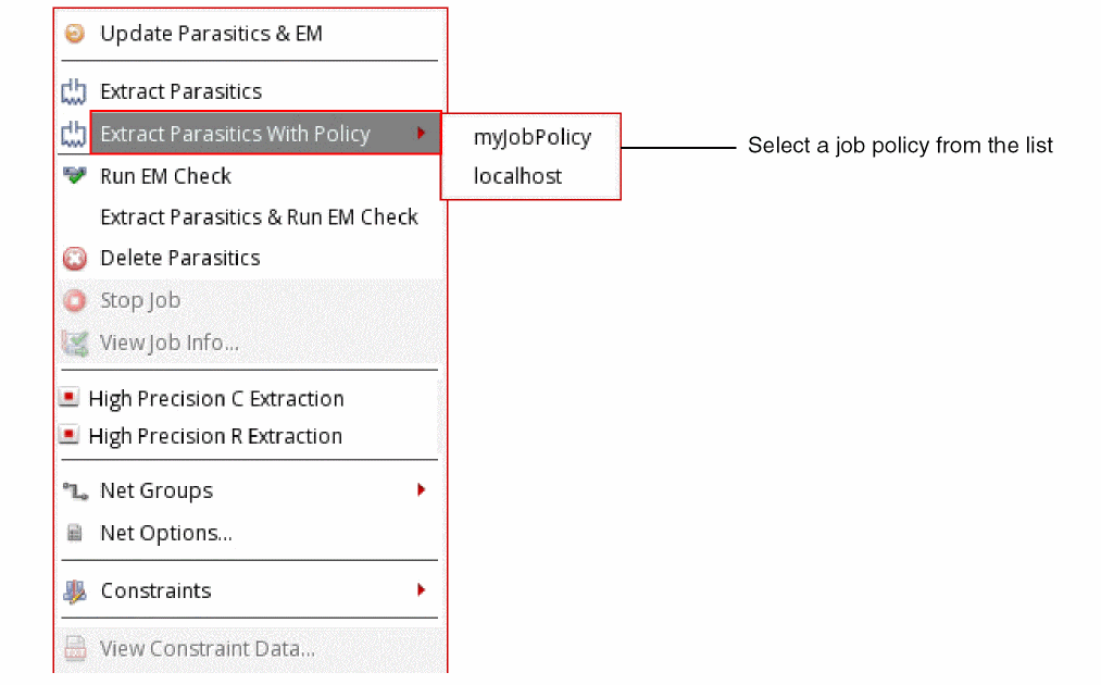
- Select the job policy that you want to use to extract parasitics. The extraction results for the selected net are updated in the Detail pane.
Job Statuses
When you submit a distributed job, an icon is displayed next to the nets. This icon indicates the current status of the submitted jobs. The following table shows the different statuses of the jobs and the corresponding icons that are displayed next to the nets for which the jobs have been submitted.
| Icon | Status of the Job |
|---|---|
Stopping a Running Job
Do the following to stop a running job that has not finished yet:
Viewing Job Information
You can view the following information about a failed job:
- Error Log: Displays information about the failed job
- Nets: Displays a list of nets for which the jobs have failed
- Output Log: Displays information such as, who submitted the job, name of host to which the job was submitted, home and working directory, time when the job was submitted
- Status: Displays the status of the jobs
- Virtuoso Log: Displays the log file for the job’s Virtuoso session
Follow these steps to view these information about the failed jobs:
-
In the Summary pane of the EAD Browser, right-click a net, and then choose View Job Info from the context menu.
The EAD Job Information form opens, as shown in the following figure.
- In the left pane, select the information that you want to view. The selected information is displayed in the right pane.
Return to top