


|
|
|||||||||
|
|
|
|
|
|
|
|
|
|
|
This chapter describes how to perform voltage regulator (VR) simulations using the Virtuoso® UltraSim™ simulator.
The conventional Virtuoso UltraSim simulator partitioning process, using ms, da, or df mode, is based on ideal supply voltages, such as dc or pwl (see "Simulation Modes and Accuracy Settings" for more information about Virtuoso UltraSim simulation modes). If a design is powered by one or multiple VRs, or the supply voltage is generated by other source types (for example, controlled sources), the Virtuoso UltraSim partitioning approach may result in large partitions and decreased simulation performance. VR simulation options can be used to resolve the performance issues produced by these applications. VR simulation is specifically designed for large mixed-signal, digital, and memory designs which are driven by regulators or other sources.
VR simulation is not applicable to pure power management blocks or designs with sensitive coupling between the generator and the driven circuit. For these applications, a mode should be used.
You need to identify the internal supply voltage nodes and driving blocks before using VR options. Supply voltage nodes are characterized by a large number of MOSFETS connected at the source nodes. Use the Virtuoso UltraSim simulator usim_report node option to identify supply voltage nodes (see "Node Connectivity Report" for more information).
Note: A period (.) is required when using SPICE language syntax (for example, .usim_vr).
Use usim_vr to run a Virtuoso UltraSim VR simulation (only applicable to circuits simulated in df, da, ms, or mx mode). A netlist file can contain multiple usim_vr commands. VR simulation produces optimal results with a strong regulator driving capacitive load and weak dc loading. Circuits with on-chip voltage regulators driving large digital blocks generally belong to this category. Table 5-1 contains all of the usim_vr commands and descriptions.
Note: You can also perform VR simulations in the Virtuoso Analog Design Environment (ADE). For more information, refer to "Setting Voltage Regulator Simulation Options" in the Virtuoso Analog Design Environment L User Guide (IC 6.1.2) or the Virtuoso Analog Design Environment User Guide (IC 5.1.41).
|
port1, port2, ... |
Note: The Virtuoso UltraSim simulator supports using wildcards (*) in instance, node, and port names.
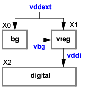
.usim_opt sim_mode=ms subckt=[bg vreg]
.usim_vr subckt=vreg node=[vddi]
In this example, the voltage regulator consists of a bandgap reference generator (bg) and the supply generator (vreg), with an internally regulated supply node (vddi). The Virtuoso UltraSim simulator usim_vr command specifies the generator blocks and internal supply nodes. Global df mode is used to simulate the circuit, and local ms mode is applied to the bg and vreg blocks.
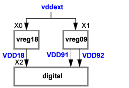
usim_opt sim_mode=df inst=[X2]
usim_vr inst=[X0 X1] node=[VDD18 VDD91 VDD92]
usim_vr inst=[X0] node=[VDD18]
usim_vr inst=[X1] node=[VDD91 VDD92]
In this example, the design contains multiple generator blocks, and the internally regulated supply nodes are VDD18, VDD91, and VDD92. The usim_vr command specifies that the X0 and X1 instances are the voltage regulator blocks, global ms mode is used to simulate the circuit (default), and local df mode is applied to the digital block.
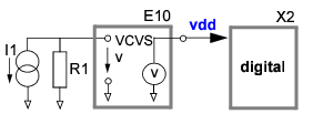
usim_vr inst=[E10 R1 I1] node=[vdd]
In this example, the voltage supply is generated by a controlled source, and the internally regulated supply node is vdd. The usim_vr command specifies the E10, I1, and R1 elements as part of the voltage regulator, global ms mode is used to simulate the circuit (default), and local df mode is applied to the digital block. The usim_vr arguments can be used in any order.
Note: You have the option to specify only one of the elements in the statement (E10, I1, or R1).
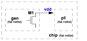
In this example, the design is a flat netlist file without subcircuit definitions. Since there are no subcircuit blocks or instances in a flat netlist file, the block option cannot be specified. To setup a VR simulation, you only need to specify one element that is part of the generator block (in this case, M1 as the transistor and vdd as the generator node). The simulator uses this information to automatically identify the block.