5
Technology File Layer Attributes
The layerRules section of the technology file specifies attributes for user-defined layers.
This chapter contains the following topics:
- layerRules
- analysisAttributeLocks
- equivalentLayers
- incompatibleLayers
- functions
- backsideLayers
- analysisAttributes
- mfgResolutions
- routingDirections
- snapPatternDefs
- relatedSnapPatterns
- widthSpacingPatterns
- widthSpacingPatternGroups
- widthSpacingSnapPatternDefs
- Current Density and Current Density Tables
- avgACCurrentDensity
- rmsACCurrentDensity
- avgDCCurrentDensity
- stampLabelLayers
- labelLayers
- cutClasses
layerRules
layerRules(
tx_recognitionLayer
) ;layerRules
Description
Contains layer rules. All subsections specifying layer rules must be enclosed within the parentheses of this section.
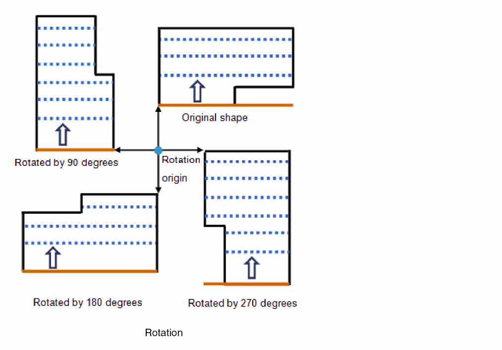
The layerOrder values should be specified in the order of the process stack, and not in the order in which layers are manufactured. For example, even if a cut layer is manufactured after its top metal layer (for example, if the process uses self-aligned vias), the layerOrder number of the cut layer should be less than that of the metal layer.
Arguments
Related Topics
analysisAttributeLocks
layerRules(
analysisAttributeLocks(
 [lockAddLayers t/nil]
 [lockValuesChange t/nil]
 ……
 ;analysisAttributeLocks
) ;layerRules
Description
Specifies analysis attribute locks on layers.
Arguments
Example
Related Topics
equivalentLayers
layerRules(
equivalentLayers(
 ( lt_layer … )
 …
) ;equivalentLayers
) ;layerRules
Description
Specifies layers that are physically and electrically equivalent or that represent the same type of material. It can be used to define layers that connect by overlap rather than through a via.
Arguments
|
A list of layers. |
Example
equivalentLayers(
    ( "metal1_supply" "metal1" )
)
Related Topics
incompatibleLayers
layerRules( incompatibleLayers( (lt_layer(lt_layer1lt_layer2… ) … ) … ) ;incompatibleLayers
) ;layerRules
Description
Lists layers, both physical and derived, incompatible with the specified physical layer. This allows exclusion of layers that do not belong to the technology graph of a technology file. By specifying a list of layer names from other incompatible versions of the process layer stack, a warning is displayed as soon as any of these layers is detected in a technology graph.
Arguments
|
A physical layer that is incompatible with the layers specified in the list that follows. The layer must be defined in the |
|
|
The derived or physical layers that are incompatible with the specified layer, and, therefore, must be excluded from the specified technology database. |
|
Example
incompatibleLayers(
   ( "metal1" ( "metal1_mid" "metal1_top") )
) ;incompatibleLayers
Specifies that metal1 is incompatible with layers metal1_mid and metal1_top. As a result, these layers are not allowed in a technology graph that contains the technology database in which the incompatibleLayers statement is specified. This allows you to model two versions of the process stack by using two technology graphs. Any accidental mixing of these two technology graphs is detected by the software.
Related Topics
functions
layerRules( functions( (t_layer|x_numbert_function[x_layerOrder] ['trims ( (t_physicalLayert_derivedLayer) … )] ) … ) ;functions
) ;layerRules
Description
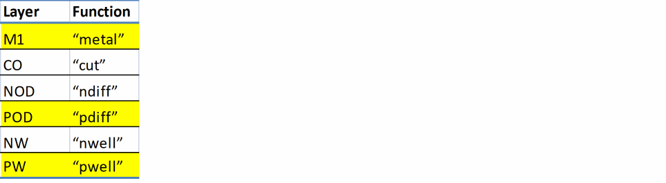
Defines layer functions (materials) and optionally assigns to layers a number that signifies the layer order. Layers assigned the function other or unknown and a layer order cannot appear in any other section of the technology file.
Multiple layers can be assigned the same layer order. Layers without an explicitly assigned layer order take the default value 0xffffffffu. The specified order is used as a proxy for the process stack by some applications such as lefout. Therefore, layers in a technology file should be ordered by the given order number, from bottom to top.
layerRules section in the technology file for Virtuoso Space-based Router is slightly more constrained. For example, it defines a unique layer order for each layer function. For more information, see the Virtuoso Space-based Router User Guide.Related Topics
Arguments
-
The
mimcaplayer material is used to designate the metal layer of a MIM (Metal/Insulator/Metal) capacitor that is not directly connected to routers. Therefore,mimcaplayers should not be added to the routervalidLayerlist. A cut layer that connectsmimcapto the routing metal above it terminates atmimcap. -
The
stackedMimcaplayer material is also used to designate the metal layer of a MIM capacitor, and should not be added to the routervalidLayerlist. However, severalstackedMimcaplayers can be placed between the routing metal layers above and below. The same cut layer that connects the routing layer above to the routing layer below can also connect to eachstackedMimcaptype layer between those routing layers. -
The
tsv(through silicon via) layer material indicates that the cut layer is a through-silicon-via cut layer. It is a vertical electrical connection passing completely through a silicon wafer. -
The
tsvMetallayer material can connect to atsvlayer or acutlayer. It is not a routing layer. -
The
padMetallayer material is the last metal layer on the front side or backside of a chip. It can connect either to acutlayer or directly to another metal layer without acutlayer in between. It can also connect to atsvlayer. It is not a routing layer. -
The
pimplantandnimplantlayers are used to generate implant masks. During post data processing, these enable you to filter thepdiffandndifflayers, which are usually drawn as a single oxide layer. -
The
passivationCutlayer material represents the cuts in the top insulating layer of the chip, known as the passivation layer. Cuts are made in the passivation layer to allow bond wires to connect to the pads below this layer. -
The
li(local interconnect) layer material defines a layer that directly contacts another layer or a set of layers without an intermediate layer with acutfunction. -
The
pdiffandndifflayer materials are used when implicit oxide definition mask is used. In implicit implantation, no dedicated layer is available for implantation, as shown below:
-
The
trimlayer material is used to specify a layer that removes material from another layer. For example, acutPolylayer that removes material from aPolylayer.The trim layer is the preferred method used by Virtuoso Space-based Router to determine the usage of cut poly operations. For technologies that do not support trim layer material, see Specifying Stop Layers in the validLayers Constraint for an alternative method. -
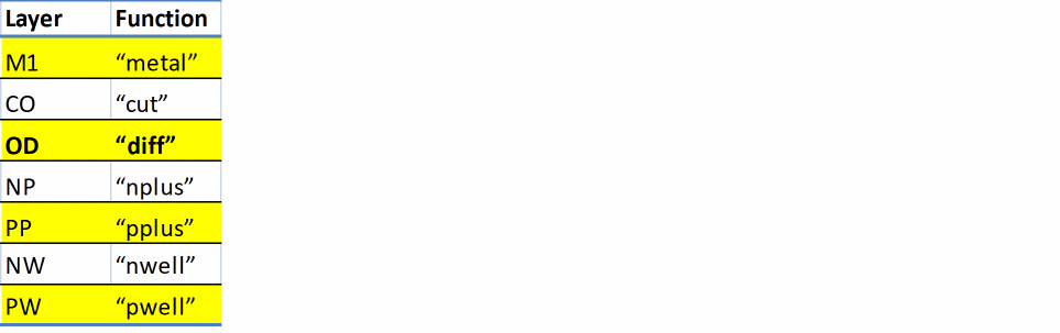
The
pplusandnpluslayer materials should be used in combination with an explicit (drawn) oxide definition mask. In explicit implantation, a dedicated layer is available to display the implantation area, as shown below:
-
The
specialCutlayer material connects one or more layers.
Example 1
functions(
    ( NWELL      "nwell"   1  )
    ( PWELL      "pwell"   2  )
    ( NDIFF      "ndiff"   3  )
    ( NPLUS      "nplus"   4  )
    ( PPLUS      "pplus"   5  )
    ( capMetal   "mimcap"  20 )
    ( throughSi  "tsv"     40 )
) ;functions
Defines layer functions and assigns a layer order to the layers.
Example 2
layerDefinitions(
    techLayers(
     ;( LayerName  Layer#  Abbreviation )
  ;( ---------  ------  ------------ )
   ( Poly         20         PO       )
   ( CutPoly      21         CP       )
 ) ;techLayers
 techDerivedLayers(
  ;( DerivedLayerName       #       composition  )
  ;( ----------------    ------     ------------ )
   ( Gate                  1000      ( Poly  'and  Active  ) )
   ( PolyInterConn         1002      ( Poly  'not  CutPoly ) )
 ) ;techDerivedLayers
) ;layerDefinitions
layerRules(
    functions(
     ;( layer     function [maskNumber])
  ;( -----     -------- ------------)
   ( Poly       "poly"     20 )
   ( CutPoly    "trim"     21  'trims  ( (Poly PolyInterConn) ) )
 ) ;functions
) ;layerRules
Defines the CutPoly layer by using the trim material type. The CutPoly layer removes material from the Poly layer. The resulting derived layer is called PolyInterConn. This is the effective Poly layer.
Example 3
techDerivedLayers(
    ( m1mask2Locked  1011  ( Metal1         'color  "mask2Color" ) 'locked )
    ( m1mask2Cut     1031  ( m1mask2Locked  'not    TM ) )
) ;techDerivedLayers
functions(
    ( Metal1  "metal"  100 )
    ( TM      "trim"   101  'trims ( (Metal1  m1mask2Cut) ) )
) ;functions
Defines an uncolored trim layer, TM, that cuts only the locked maskColor2 shapes on Metal1.
Example 4
techDerivedLayers(
    ( m1mask1        1011     ( Metal1   'color  mask1Color) )
    ( m1mask2        1012     ( Metal1   'color  mask2Color) )
    ( TMmask1        1021     ( TM       'color  mask1Color) )
    ( TMmask2        1022     ( TM       'color  mask2Color) )
    ( m1mask1Cut     1031     ( m1mask1  'not    TMmask1   ) )
    ( m1mask2Cut     1032     ( m1mask2  'not    TMmask2   ) )
) ;techDerivedLayers
functions(
    ( Metal1  "metal"  100 )
    ( TM      "trim"   101  'trims ( (Metal1 m1mask1Cut) (Metal1 m1mask2Cut) ) )
) ;functions
Defines a colored trim layer, TM. Trim shapes on TM with mask1Color cut mask1Color shapes on Metal1 and trim shapes on TM with mask2Color cut mask2Color shapes on Metal1.
Related Topics
backsideLayers
layerRules(
backsideLayers(
 tx_layer …
) ;backsideLayers
) ;layerRules
Description
Specifies the layers that are used on the backside of a wafer. These layers are used to form the bottom layer of through-silicon-vias (TSV).
Arguments
|
The layers that are used on the backside of a wafer. |
Example
layerRules(
    backsideLayers(
     MB
 ) ;backsideLayers
) ;layerRules
Defines layer MB as a backside metal layer.
Related Topics
analysisAttributes
layerRules( analysisAttributes( (tx_layer['materialNamet_materialName] ['thicknessf_thickness] ['conductivityf_conductivity] ['permittivityf_permittivity] ['lossTangentf_lossTangent] ) ) ;analysisAttributes
) ;layerRules
Description
Specifies the names and related attributes of the materials used to manufacture a layer.
Arguments
|
The layer for which the attributes are specified. |
|
Example
layerRules(
    analysisAttributes(
     ( M1  'materialName      "MX"
    'thickness        23
  )
  ( M2  'materialName      "MX"
    'conductivity    6e7
    'thickness        23
  )
 ) ;analysisAttributes
) ;layerRules
Defines material attributes for two layers:
-
For
M1layer: material nameMXand thickness23microns. -
For
M2layer: material nameMX, conductivity as6e7Siemens/meter, and thickness as23microns.
Related Topics
mfgResolutions
layerRules( mfgResolutions( (tx_layerg_value) … ) ;mfgResolutions
Description
Specifies that grid snapping for the specified layer must be a multiple of the specified value.
This constraint (layer manufacturing grid resolution) can be applied to any layer. If it is not specified for a layer, the overall mfgGridResolution constraint applies.
Arguments
|
The layer on which the constraint is applied. |
|
|
The manufacturing grid resolution for the layer. |
Example
mfgResolution(("metal1" 0.001000)("poly1" 0.000500))
Sets the layer manufacturing grid resolution to 0.001000 for layer metal1 and to 0.00500 for layer poly1.
Related Topics
routingDirections
layerRules( routingDirections( (tx_layerg_direction) … ) ;routingDirections
) ;layerRules
Description
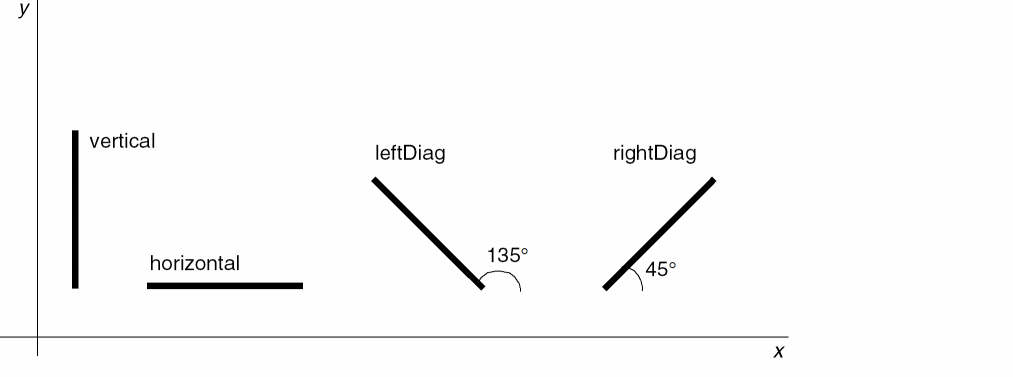
Sets the preferred routing direction for each specified layer.
The direction specified by this layer attribute is the preferred routing direction for the layer. The possible routing directions are illustrated in the figure below:
Arguments
Example
layerRules(
    routingDirections(
     ( "metal1" "horizontal")
  ( "metal2" "vertical")
  ( "diff"   "none")
  ( "via1"   "notApplicable")
 )
) ;layerRules
Sets the routing direction for metal1 to horizontal, for metal2 to vertical, for diff to none, and for via1 to notApplicable.
Related Topics
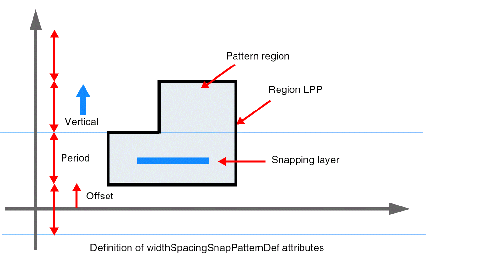
snapPatternDefs
layerRules( snapPatternDefs( (t_name(tx_layer tx_purpose) 'stepg_step'stepDirection {"horizontal" | "vertical"} ['type {"local" | "global"} ] ['offsetg_offset] ['snappingLayers ( ('layertx_snapLayer… 'enclosuresf_enclosure… ['purposestx_snapPurpose…] ['snappingMode {"multiTrackCenter" | "singleTrackCenter"}] ['exceptOverlapl_overlapLPPs] ) … ) ['trackWidthg_trackWidth] ['trackGroups ( ('countn_trackCount'spacex_groupSpace) … ) ] ) ) ;snapPatternDefs
) ;layerRules
Description
(Virtuoso Advanced Node for Layout Standard) Specifies the grid information stored in the technology database for a specific layer-purpose pair (LPP). Each snap pattern definition must have a unique name and be associated with a unique LPP. Snap pattern definitions can be local or global.
A shape drawn on an LPP with a snap pattern definition is referred to as a snap pattern shape.
The following figures illustrate the various attributes of a snap pattern:
Activating a Global Snap Pattern Definition
A global snap pattern definition applies to the entire cellview. It can be activated through a:
Snap Pattern Shape
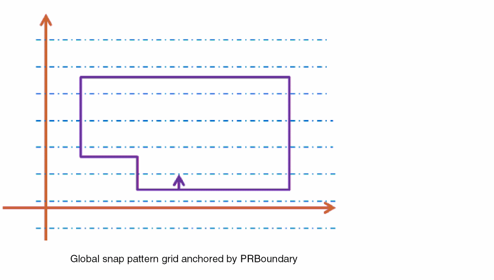
A global snap pattern definition is activated when a snap pattern shape is drawn on an LPP with a global snap pattern definition. In the figure below, the snap pattern shape is shown in orange. The grid offset, indicated by the arrow, is relative to the bottom edge (for vertical direction) or the left edge (for horizontal direction) of the snap pattern shape.
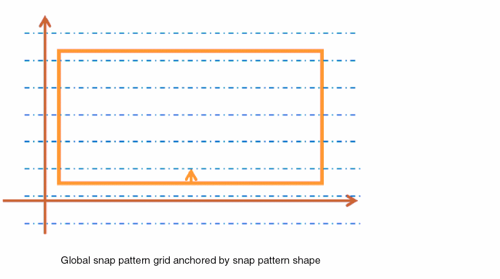
Global snapPatternDef
When the snap pattern definition is enabled through the
For more information about how to control the anchoring of global snap pattern definitions, see
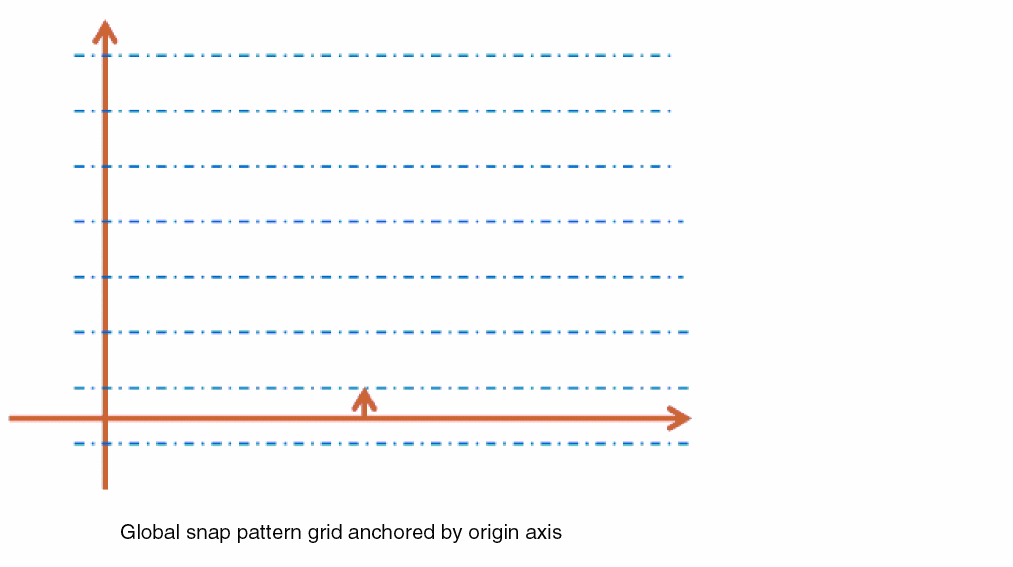
If neither a snap boundary nor a PRBoundary exists and no shape is drawn on a global grid LPP, the grid is anchored to the origin axis (X-axis for the vertical direction, Y-axis for the horizontal direction), as shown in the following figure:
Track Groups
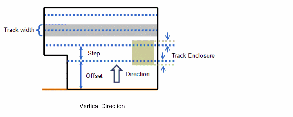
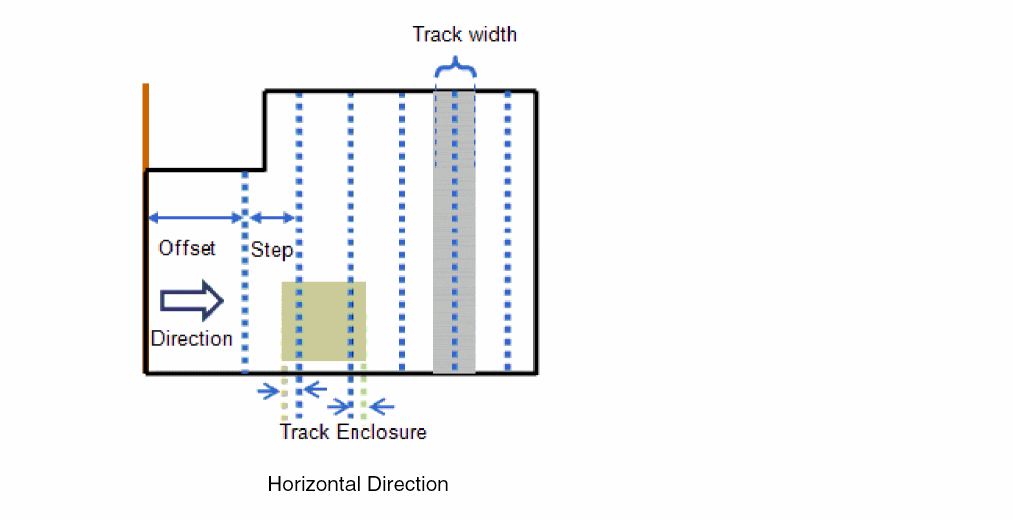
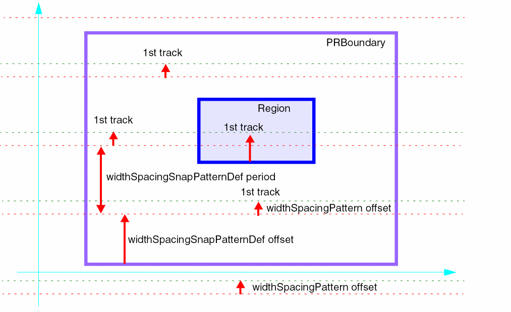
(Virtuoso Advanced Node for Layout Only) This feature lets you create track groups with variable spacing. Additionally, each track group in the snap pattern definition can contain a different number of tracks. For example, in the figure below, the bottom track group has three tracks and the top track group has four tracks. The track enclosure is set to half the track width, resulting in snap pattern shapes (in green) that enclose the track width.
This example also shows how track groups are positioned. The distance from the reference edge to the centerline of the first track is equal to the snap pattern definition offset, and each group has its own spacing that specifies the distance between the last track in the current group and the first track in the next group.
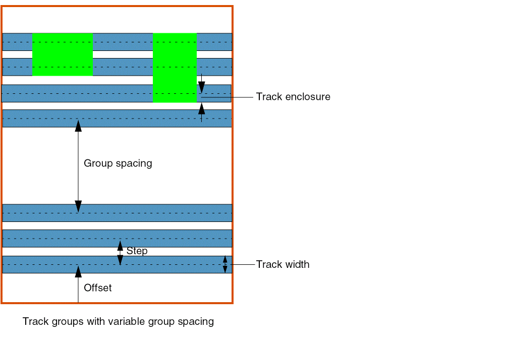
Within each group, the 'step attribute defines track-to-track spacing, and the 'trackWidth attribute defines the width of each track. Snap pattern shapes enclose tracks by using the 'enclosures attribute.
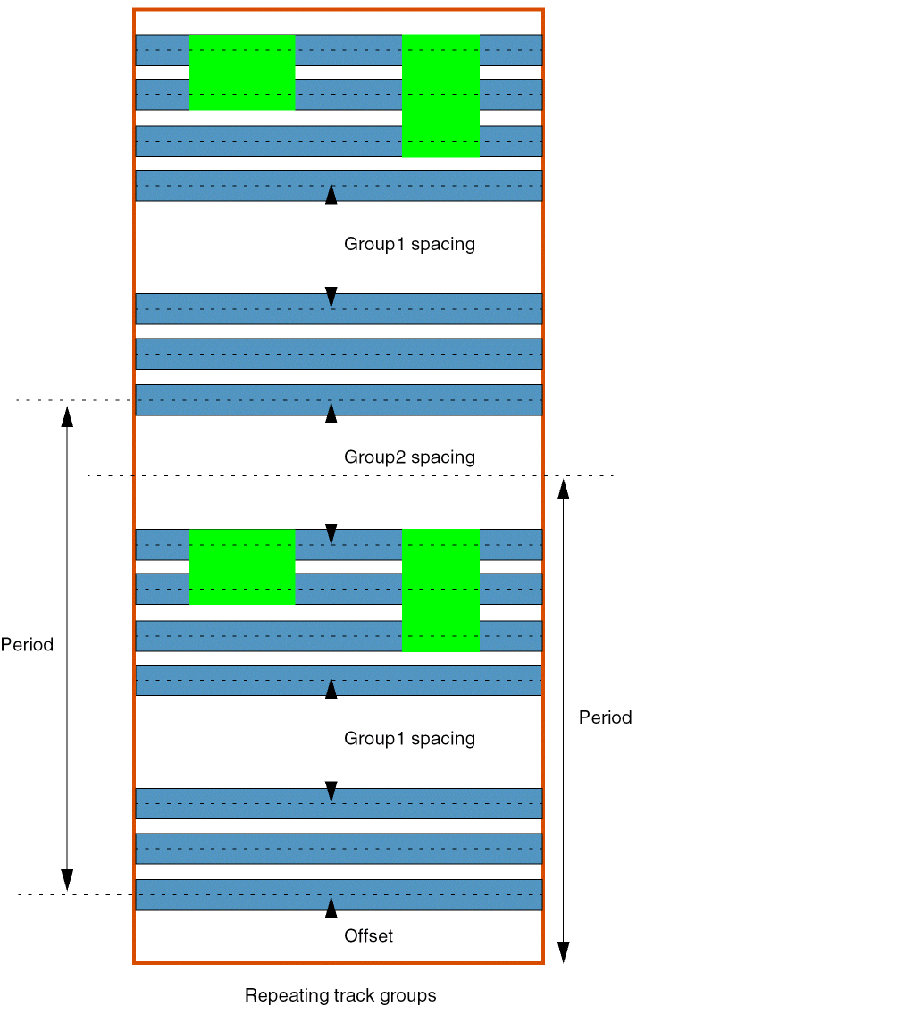
Track groups defined in a snap pattern definition are repeated to fill snap pattern shapes of arbitrary sizes. The period in this case is defined as the total height of one repetition of the full snap pattern definition and is calculated as follows:
Track group height, GT = groupSpace + (trackCount - 1) * step
For example, in the figure below, you can see two repetitions of a snap pattern with two track groups. The spacing of the last track group is used when a snap pattern is tall enough to accommodate a repetition of the pattern, that is, the spacing of the last track group is the distance from the last track in the last track group to the first track in the first track group.
Arguments
Example
layerDefinitions(
     techPurposes(
   (fb       1001 fb   'parent annotation)
   (fbdummy  1002 fbd  'parent annotation)
  ) ;techPurposes
) ;layerDefinitions
layerRules(
     snapPatternDefs(
   (finfet     ("FF" "fb")
   'offset           0.007
   'type             "local"
   'step             0.048
   'stepDirection    "vertical"
   'snappingLayers   (
    ('layer "Active" 'enclosures (0.007)
    'snappingMode "singleTrackCenter"
    'exceptOverlap ("GG" "Purp1")
    )
   )
   'trackWidth       0.014
   )
   (finfetDummy ("FF" "fbdummy")
   'offset           0.007
   'type             "local"
   'step             0.048
   'stepDirection    "vertical"
   'snappingLayers   (
    ('layer "Active"
    'enclosures (0.007)
    'purposes ("dummy" "dummy1")
    )
   )
   'trackWidth        0.014
   )
 ) ;snapPatterns
) ;layerRules
Related Topics
relatedSnapPatterns
layerRules( relatedSnapPatterns( (t_name'snapPatternDefs ( (t_snapPatternDefName['patterns (l_patternNames)] ['patternGroups (l_patternNames)] ) …) ['extraLPP (tx_layertx_purpose)] ['regionSnapPitchHorizontalf_snapH] ['regionSnapPitchVerticalf_snapV] ) ) ;relatedSnapPatterns
) ;layerRules
Description
(Virtuoso Advanced Node for Layout Only) Specifies predefined groupings of snapPatternDefs and widthSpacingSnapPatternDefs used to create groups of regions in the layout. The allowed patterns and pattern groups on each region in the group are initialized to the values specified by the 'patterns and 'patternGroups attributes. The active pattern of the region is set to the first pattern in the 'patterns attribute list.
Patterns and groups are specified only for widthSpacingSnapPatternDefs. These attributes are not used for snapPatternDefs.
Arguments
Example
relatedSnapPatterns(
    ("1XGroup"
     'snapPatternDefs (
   ("fb1")
   ("m1_grid" 'patterns ("1X" "1X-4X"))
   ("m2_grid" 'patterns ("1X"))
   ("m3_grid" 'patterns ("1X-3X" "1X-4X"))
  )
  'extraLPP ("Active" "drawing")
  'regionSnapPitchHorizontal 0.1
  'regionSnapPitchVertical 0.2
 )
) ;relatedSnapPatterns
Specifies a relatedSnapPatterns definition named 1XGroup. It contains entries for four grids: the fin grid, fb1, and the routing grid for m1, m2, and m3. When a region group is created using this definition, it would contain four shapes—one for each grid. The allowed patterns on the m1_grid region would be set to 1X and 1X - 4X. An additional LPP is specified along with related pitch values.
Related Topics
widthSpacingPatterns
layerRules( widthSpacingPatterns( (t_name['offsetg_offset['repeatOffset]] ['startingColorg_maskColors| 'shiftColor] ['allowedRepeatMode {"any" | "none" | "steppedOnly" | "flippedOnly"} ['defaultRepeatMode {"stepped" | "flippedStartsWithOdd" | "flippedStartsWithEven"} ] ] 'pattern( (['repeatg_repeat] ['wireTypes (l_wireTypes)] ['colors (g_colors…)] ['displayPackets (l_packets)] 'spec(('widthg_width'spaceg_space['wireTypet_wireType] ['colorg_maskColors] ['displayPackett_packet] ) … ) ;spec ) … ) ;pattern ) ) ;widthSpacingPatterns
) ;layerRules
g_colors := "mask1Color" | "mask2Color" | "mask3Color" | "grayColor"
g_maskColors := "mask1Color" | "mask2Color" | "mask3Color"
Description
(Virtuoso Advanced Node for Layout Only) Defines the tracks on which shapes can be placed. It also defines the width of shapes on those tracks. Each pattern may span one or multiple periods. A widthSpacingPattern (WSP) by itself has no layer and no direction. It defines the width, spacing, and, optionally, the color and the wire type for a set of tracks. The pattern is then applied to a routing layer in a particular direction by specifying it as the active pattern in a widthSpacingSnapPatternDef.
Each track can have an optional wire type, which is a string label that can be used to refer to tracks by a name. During layout editing, tracks can be enabled or disabled through wire type filtering.
There are two ways to specify the color of each track in a pattern. In most cases, tracks have alternating colors and no adjacent pair of tracks has the same color. This can be specified by using the 'startingColor attribute. This attribute specifies the color of the first track; all other tracks are colored automatically with alternating colors.
In certain situations, not all tracks are colored or adjacent tracks need to be assigned the same color. This can be done by using the 'color attribute of each individual track or by using the 'colors attribute to specify a list of colors for a set of tracks. In addition, the 'shiftColor attribute can be used to specify whether all track colors are shifted when the pattern repeats, or whether each repetition of the pattern has the same color assignment.
As shown in the figure below, each widthSpacingPattern is a sequence of width-space pairs. The offset indicates the location of the first track from the period grid.
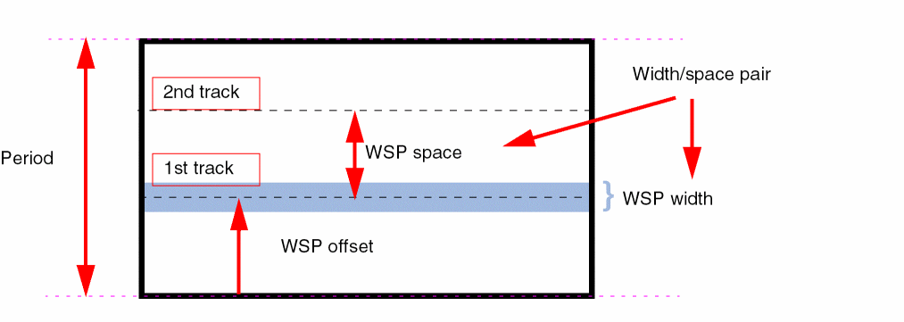
A collative view of the widthSpacingSnapPatternDef offset and the widthSpacingPattern offset is illustrated in the figure below:
The red dotted lines indicate the global period grid in each stripe of the period grid. This grid is anchored to the PRBoundary by using the offset of the widthSpacingSnapPatternDef.
The green dotted lines indicate the first track in each period. Outside pattern regions, the active global default pattern is applied and its offset specifies the distance from the period grid line to the first wiring track.
Finally, a region shape is used to apply a non-default active pattern in an area of the cellview. The active pattern specified on the region overrides the default active pattern and its offset specifies the location of the first track.
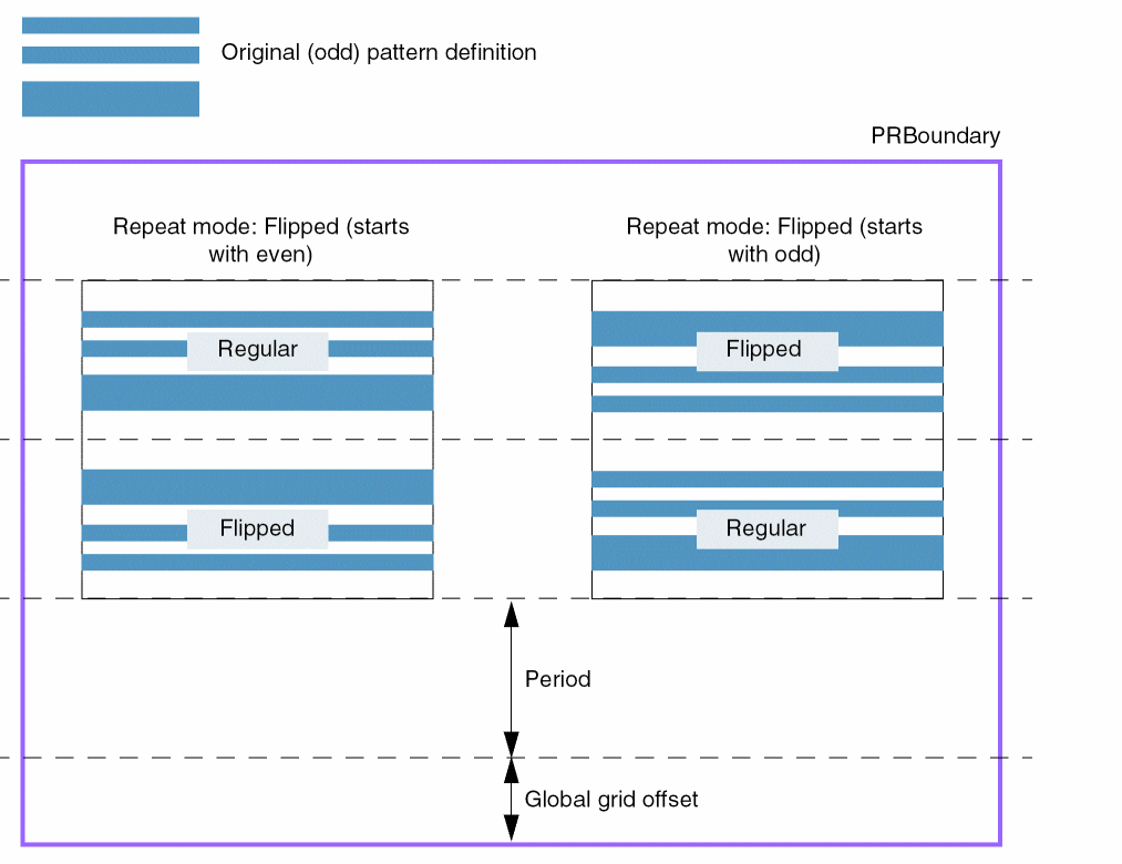
Repeat Modes and Pattern Flipping
Repeat modes determine how a pattern is interpreted for use in adjacent periods. The allowed and default repeat modes are specified on a widthSpacingPattern; the repeat mode can be specified in the layout on global grids and pattern regions.
The 'allowedRepeatMode attribute indicates how a pattern is allowed to repeat when a region stretches across more than one period, and the 'defaultRepeatMode attribute is used to initialize the repeat mode on regions and global grids when they are first created.
The following are valid combinations for allowed repeat mode ('allowedRepeatMode) and default repeat mode ('defaultRepeatMode) attributes:
| Allowed repeat mode | Default repeat mode |
-
A repeat mode can be defined at the following two levels:
- On a region: A region has a set of allowed patterns and a repeat mode can be specified for each pattern.
-
On a global grid: Each global grid also has a set of allowed patterns and a repeat mode can be specified for each pattern. A global grid in a cellview is identified by a global
widthSpacingSnapPatternDef(the one that is set as active in the Track Pattern Assistant).
- A repeat mode defined on a global grid or a pattern region can be of one of the following types:
A repeat mode is not inherited and does not have a look-up precedence. As a result, when the repeat mode of the global grid changes, the regions on that global grid are not affected. However, when a region with a pattern for which the repeat mode is set is copied, the repeat mode is also copied to the newly created region.
The following example illustrates how a pattern in a region appears when "even" and "odd" flipped repeat modes are applied to the pattern:
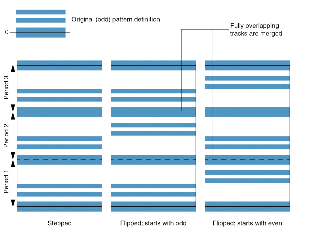
Patterns with Zero Offset
When a pattern has zero offset, the centerline of the first track is located on the period line or the bottom edge of the region. In a legal pattern, the height of the pattern needs to be compatible with the period and the height of the region. Therefore, a track at offset zero is also present on the top period line or the top region boundary. When a pattern with zero offset is flipped, the top and bottom tracks overlap and are merged into one single track.
The following example illustrates how a pattern with zero offset appears when "even" and "odd" flipped repeat modes are applied to the pattern in a region:
Arguments
Example 1
layerRules(
widthSpacingPatterns(
 ("2-1x-1-2x"
  'offset 0.05
  'repeatOffset
  'startingColor "mask1Color"
  'pattern(
   (
    'repeat 2
    'spec (('width 0.04   'space 0.1))
   )
   (
    'spec (('width 0.08   'space 0.1))
   )
  )
 )
) ;widthSpacingPatterns
) ;layerRules
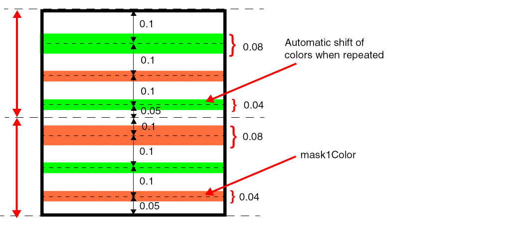
Specifies that the tracks are alternately colored and are shifted on repeat because the number of tracks in the pattern is odd.
Example 2
layerRules(
    widthSpacingPatterns(
     ("1-1x-1-2x"
   'offset 0.05
   'repeatOffset
   'startingColor "mask1Color"
   'pattern (
    (
     'repeat 2
     'spec  (
      ('width 0.04   'space 0.2)
      ('width 0.08   'space 0.1)
     )
    )
   )
  )
 )
) ;layerRules
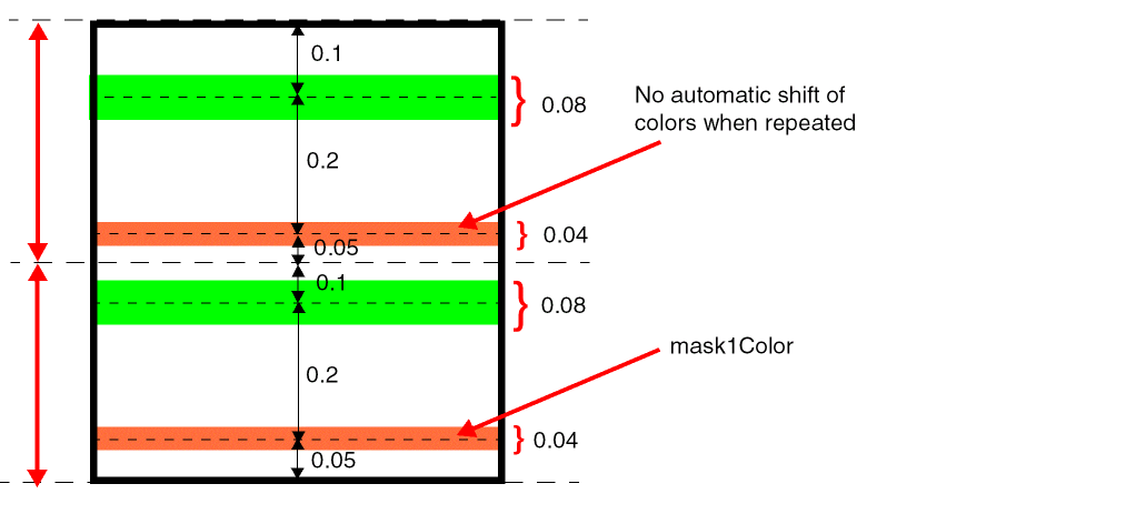
Specifies that the tracks are alternately colored, but are not shifted on repeat because the number of tracks in the pattern is even.
Example 3
layerRules(
    widthSpacingPatterns(
     ("2-1x-1-2x"
   'shiftColor
   'offset 0.05
   'repeatOffset
   'pattern (
    (
     'repeat 2
     'colors ("mask1Color" "mask1Color")
     'spec (('width 0.04   'space 0.1))
    )
    (
     'spec  (('width 0.08 'space 0.1 'color "mask2Color"))
    )
   )
  )
 )
) ;layerRules
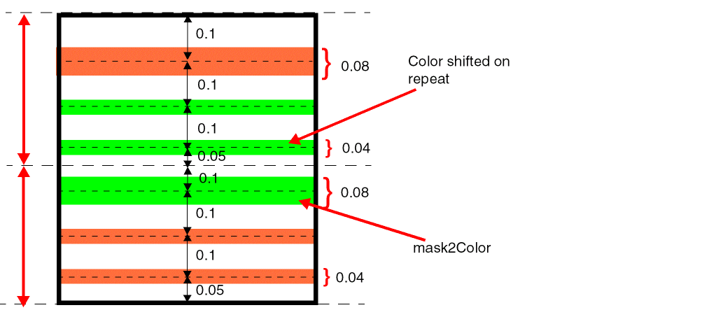
Specifies that the tracks are colored individually and some adjacent tracks have the same color. When the pattern is repeated, the colors are shifted because the 'shiftColor attribute is used.
Example 4
layerRules(
    widthSpacingPatterns(
     ("2-1x-1-2x"
   'shiftColor
   'offset 0.05
   'pattern (
    (
     'repeat 2
     'colors ("mask1Color" "mask1Color")
     'spec (('width 0.04   'space 0.1))
    )
    (
     'spec  (('width 0.08 'space 0.15 'color "mask2Color"))
    )
   )
  )
 )
) ;layerRules
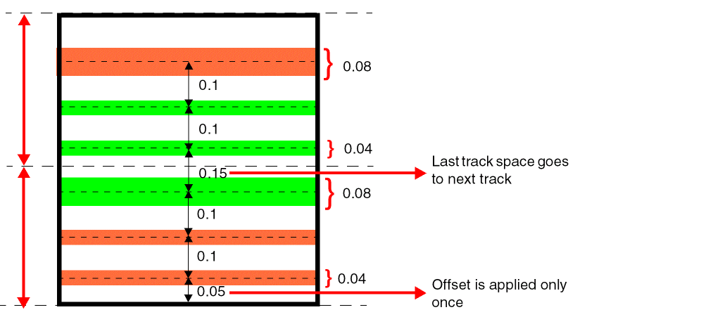
Specifies that the offset is applied only once because 'repeatOffset is not given. The spacing specified for the last track in the pattern goes to the next track, as shown.
Related Topics
widthSpacingPatternGroups
layerRules( widthSpacingPatternGroups( (t_name'members (l_patternNames) ) … ) ;widthSpacingPatternGroups
) ;layerRules
Description
(Virtuoso Advanced Node for Layout Only) Defines groups of widthSpacingPatterns specified in the technology file. Such a group is a convenient way to refer to a set of patterns by name. Groups can be used in a set of allowed patterns on a widthSpacingSnapPatternDef and region shapes.
Arguments
|
The list of width spacing patterns names that are members of this group. |
|
Example
layerRules(
    widthSpacingPatternGroups(
     ( "basic"
   'members ( "minWidth" "2XWidth")
  )
  ( "multiWSP"
   'members ( "WSP1" "WSP2" )
  )
 )
) ;layerRules
Defines pattern groups basic and multiWSP. Each group has two patterns as members.
Related Topics
widthSpacingSnapPatternDefs
layerRules( widthSpacingSnapPatternDefs( (t_name(tx_layer tx_purpose) |tx_layer'periodg_period'direction "vertical" | "horizontal" ['offsetg_offset] ['snappingLayers( ('layertx_snapLayer['purposesl_purposes]) … ) ] {['patterns (l_patternNames)] ['patternGroups (l_patternGroupNames)] } 'defaultActivet_defaultActivePatternName['orthogonalGridg_gridType['orthogonalGridColor "mask1Color" "mask2Color" "mask3Color" "mask4Color"] ) ) ;widthSpacingSnapPatternDefs
) ;layerRules
Description
(Virtuoso Advanced Node for Layout Only) Defines a coarse-grain grid called the period grid in a cellview. The available wiring tracks are specified between the period grid lines using width spacing patterns. By default, the default active pattern applies in every period stripe. Rectangles and polygons on the widthSpacingSnapPatternDef's LPP can be used to customize the width spacing patterns in a particular area of the cellview. Such rectangles and polygons are referred to as "regions".
widthSpacingSnapPatternDefs also define a set of allowed patterns and pattern groups. All shapes on the snapping layers must conform to one of these allowed patterns. Regions can be used to override the default set of allowed patterns and pattern groups in certain areas of the cellview.
The snapping layers are the layers to which the widthSpacingSnapPatternDef applies. Typically, one widthSpacingSnapPatternDef is used per routing layer.
The direction of a widthSpacingSnapPatternDef is the direction in which the spacing between period grid lines is measured, that is, a vertical widthSpacingSnapPatternDef would have horizontal period lines.
The global period grid defined by a widthSpacingSnapPatternDef is anchored to the lower edge, along with an optional offset, of the SnapBoundary or PRBoundary. If a SnapBoundary or PRBoundary does not exist, the global grid is anchored to the origin axis. This behavior can be disabled using the dbSetGlobalGridOffsetReferenceType function.
A widthSpacingSnapPatternDef applies to a cellview only if it is enabled through a snapGridVertical or snapGridHorizontal constraint. This constraint can be specified library-wide in the foundry constraint group or in a cellview's default constraint group.
The following figure illustrates the coarse-grain period grid with vertical direction, anchored to the origin axis.
Arguments
Example
widthSpacingSnapPatternDefs(
    ( M2WSP
     ("Metal2"       "localWSP")
  'period         0.768
  'direction      "vertical"
  'offset         0
  'snappingLayers ( ('layer Metal2) )
  'patterns       ("stdCell")
  'patternGroups  ("basic" "multiWSP")
  'defaultActive  "minWidth"
 )
)
Defines a widthSpacingSnapPatternDef named M2WSP that specifies a vertical period grid in which each stripe is 0.768 high. The first period grid line falls on the lower edge of the PRBoundary, or the origin axis, because the offset is zero.
This widthSpacingSnapPatternDef applies to the Metal2 routing layer. By default, the minWidth pattern is shown in each stripe. The default set of allowed patterns includes all patterns in the basic and multiWSP groups, as well as the stdCell pattern. The active and allowed patterns can be customized by creating region shapes on the Metal2/localWSP LPP.
Related Topics
Current Density and Current Density Tables
Current density tables allow conditional evaluation and application of a layer attribute value by means of lookup tables. When specifying current density tables, you must follow the syntax indicated. Current density tables always apply to one layer and can be one- or two-dimensional, with the attribute value being determined by one or two other design values. All currentDensityTable attributes must be specified as indicated in their syntax statements.
The table specification (l_table) always takes the following syntax:
|
|
|
where, an index is a value for the design value being used to determine the attribute value.
- The table entries must be specified in the ascending order.
-
All table entries must be explicitly specified; otherwise, the technology file compiler uses the default value for the unspecified entries. If no default value has been specified in the
currentDensityTablessection, the compiler fills in a0for the missing entries in the table. -
Each table entry is read as greater than or equal to. For example, consider the following table entries:
currentDensityTables(
 ( peakACCurrentDensity "Metal1"
  (( "frequency" nil nil ))
  ( list(
    (1       5e-07)
    (2e+08   4e-07)
   )
  )
 )
) ;currentDensityTables
If the index design value (frequency) is greater than or equal to1, the layer attribute value is5e-07; if the index design value is greater than or equal to2e+08, the attribute value is4e-07. The value returned is the first value in the table that matches a query of the lookup table.
techParam(paramName)).peakACCurrentDensity
layerRules( currentDensity( ( peakACCurrentDensitytx_layerf_value) … ) ;currentDensity currentDensityTables( ( peakACCurrentDensitytx_layer(( "frequency" nil nil ["width" | "cutArea" nil nil] ) [f_default] ) (g_table) ) … ) ;currentDensityTables
) ;layerRules
Description
Sets the peak AC current density for the specified layer, absolutely or conditionally, as a function of the frequency (1-D table) or frequency and width of the object (2-D table) on the layer. The value specified by this rule is the maximum (peak) AC current that an object on the layer can handle.
Arguments
Related Topics
avgACCurrentDensity
layerRules( currentDensity( ( avgACCurrentDensitytx_layerf_value) … ) ;currentDensity currentDensityTables( ( avgACCurrentDensitytx_layer(( "frequency" nil nil ["width" | "cutArea" nil nil] ) [f_default] ) (g_table) ) … ) ;currentDensityTables
) ;layerRules
Description
Sets the average AC current density for the specified layer, absolutely or conditionally, as a function of the frequency (1-D table) or frequency and width of the object (2-D table) on the layer. The value specified by this rule is the average AC current that an object on the layer can handle.
Arguments
Related Topics
rmsACCurrentDensity
layerRules( currentDensity( ( rmsACCurrentDensitytx_layerf_value) … ) ;currentDensity currentDensityTables( ( rmsACCurrentDensitytx_layer(( "frequency" nil nil ["width" | "cutArea" nil nil] ) [f_default] ) (g_table) … ) ) ;currentDensityTables
) ;layerRules
Description
Sets the root mean square (RMS) AC current density for the specified layer, absolutely or conditionally, as a function of the frequency (1-D table) or frequency and width of the object (2-D table) on the layer. The value specified by this rule is the maximum RMS AC current that an object on the layer can handle.
Arguments
Related Topics
avgDCCurrentDensity
layerRules( currentDensity( ( avgDCCurrentDensitytx_layerf_value) … ) ;currentDensity currentDensityTables( ( avgDCCurrentDensitytx_metalLayer(( "width" nil nil ) [f_default] ) (g_table) ) ( avgDCCurrentDensitytx_cutLayer(( "cutArea" nil nil ) [f_default] ) (g_table) ) ) ;currentDensityTables
) ;layerRules
Description
Sets the average DC current density for the specified layer, absolutely or conditionally, as a function of the width or the area of the object. The value specified by this rule is the average DC current that an object on the layer can handle.
Arguments
Related Topics
stampLabelLayers
layerRules( stampLabelLayers( (textLayerlayers) … ) ;stampLabelLayers
) ;layerRules
Description
Defines a rule for creating a label on a particular layer-purpose pair. It specifies text (label) layers and the corresponding layer-purpose pair (LPP) entries of connected type associated with them.
The text name is considered as the name of the electrical node when the text origin is on or inside a shape on one of the listed layers. A label with an origin that is positioned over multiple conducting layers is applied to the first layer or LPP in the layer list; that is, the first layer or LPP specified in the list takes the highest precedence and the last one takes the lowest precedence.
Arguments
|
The layer associated with the subsequently specified layers of connected type. |
|
Example
stampLabelLayers(
    ( Metal1 (Metal1 fill) )
    ((Metal2 pin) Metal2)
    ( Text (Metal2 pin) Metal2 (Metal1 pin) Metal1)
) ;stampLabelLayers
The first layer-purpose pair entry of a rule indicates the layer-purpose pair on which the label is created for a shape that exists on layer-purpose pairs defined by the remaining entries of the rule.
Related Topics
labelLayers
layerRules( labelLayers( (tx_lableLayer1tx_conLayer1[tx_conLayer2… ] ) (tx_labelLayer2tx_conLayer… ) … ) ;labelLayers
) ;layerRules
Description
Specifies how text on label layers and the layers of any type associated with them should be handled.
The text name is not considered for naming electrical nodes. The label is associated with the first layer that has a shape that touches or overlaps the text. This specification provides a systematic means for establishing parent (shape)/child (text) relationships that are more general than a standard database parent/child relationship; with the labels relationship, the parent could be lower in the hierarchy and can be one of many layers.
Arguments
|
The layer associated with the subsequently specified layers. |
|
Example
labelLayers(
    ( text Metal17 Metal16 Metal15 Poly Oxide )
) ;labelLayers
Related Topics
cutClasses
layerRules( cutClasses( [t_name] (tx_cutLayer(t_cutClassName['numCutsx_numCuts] ['minWidth] ['minLength] ['fixedOrientation] ['cutClassGroupsl_groups] {f_width| (f_widthf_length) } ) ;t_cutClassName… ) ;tx_cutLayer… ) … ) ;cutClasses
) ;layerRules
Defines a cut class by specifying the exact width and length the members of that cut class can have on a layer. Each cut class on a layer is assigned a unique name by which it can be referenced. If length for a cut class is not specified, cut shapes belonging to that cut class are squares with both dimensions equal to the specified width.
The value numCuts defines the equivalent number of via cuts required to satisfy the minNumCut constraint and to calculate the resistance. If the equivalent number of via cuts is x and minNumCut requires n via cuts, minNumCut is satisfied if n/x rounded up to the nearest integer is greater than or equal to n. For example, if the equivalent number of cuts is 2 and minNumCut requires 2 via cuts, then 1 via cut would be sufficient to satisfy minNumCut.
Cut class constraints can be defined only in a technology database.
A technology file can include multiple cutClass sections, each within a uniquely named constraint group. A cutClass section can be used without a name to indicate that the cutClass definitions in it be used to resolve cutClass references in constraints in the foundry constraint group. If all cutClass sections are named, the cutClass definitions in the last cutClass section are used to resolve such references.
Naming cutClass sections can be useful when defining a set of cut classes to be used in an alternate foundry constraint group. The named cutClass constraint group can be added as a member constraint group in another constraint group, which in turn, can be used as an alternate foundry constraint group.
Cut class constraints are referenced by other constraints to restrict these other constraints to apply only to cut shapes of the specified size on the specified cut layer. For example, in some processes, different allowed spacings are required for via cuts on a layer depending on the sizes of the via cuts.
All cut class constraints for cut layers defined in a single technology database must be added in one OR constraint group, which, in turn, must be a member of the foundry constraint group in the same technology database. The technology file loader creates a constraint for each cut class defined in the technology database and adds all of these constraints to a constraint group with the name cutClass_<libName>, which is the name used when t_name is not specified. If cut classes are defined in different technology databases contained in an ITDB, all cut classes are considered to be part of the same effective OR constraint group.
If multiple cut classes with the same dimensions exist in the technology database, the cut class names in the minCutClassSpacing (One layer) and minCutClassSpacing (Two layers) constraints in the dumped technology file are not the same as in the input technology file. The technology dumper randomly picks any one name.
Values
|
The width and length of cut shapes belonging to the cut class must be equal to these values. |
|
Parameters
Examples
- Example 1: cutClasses with numCuts, minWidth, and minLength
- Example 2: cutClasses with cutClassGroups
Example 1: cutClasses with numCuts, minWidth, and minLength
You can define all cut classes for a given layer together, as shown below. Four cut classes, namely, VA, VB, VC, and VD, are created in this example.
layerRules(
cutClasses(
;( layerName )
;( (cutClassName (width length)) )
;( -------------------------------------------------------------- )
  ( Via1
   ( VA (0.3 0.4) )
   ( VB 'numCuts 2 (0.4 0.6) )
   ( VC 'minWidth 'minLength (0.8 0.7) )
   ( VD (0.3 0.3) )
  )
  ( Via3
   ( VA (0.4 0.3) )
   ( VB 'numCuts 2 (0.5 0.6) )
   ( VC 'minWidth 'minLength (0.8 0.7) )
   ( VD (0.4 0.4) )
  )
) ;cutClasses
) ;layerRules
Example 2: cutClasses with cutClassGroups
You can define constraint groups as shown below. Two cut class groups, named g1 and g2, are defined in this example.
A viaStack application would pick one member on each layer. For g1, it can pick V0A, V1A, V2A or V0A, V1B, V2A. Whereas, for g2, it would pick V0A, V1C, V2B. If a constraint is specified on layer Via1, group g1 would refer to V1A and V1B.
cutClasses(
     ( V0
   (V0A 'numCuts 1 'cutClassGroups ("g1" "g2") (0.034 0.034))
  )
  ( Via1
   (V1A 'numCuts 1 'cutClassGroups ("g1") (0.034 0.034))
   (V1B 'numCuts 2 'cutClassGroups ("g1") (0.07  0.034))
   (V1C 'numCuts 2 'cutClassGroups ("g2") (0.07  0.034))
  )
  ( Via2
   (V2A 'numCuts 1 'cutClassGroups ("g1") (0.05 0.05))
   (V2B 'numCuts 2 'cutClassGroups ("g2") (0.1  0.05))
  )
) ;cutClasses
Accessing Cut Class Information Using SKILL
You can access information about cut classes from the technology file using SKILL. To do this, you need to perform the following steps:
-
Obtain
techIDfrom an open cellview; for example:cv = geGetEditCellView()
tf = techGetTechFile(cv)
Or, obtaintechIDby specifying the technology library name; for example:tf=techGetTechFile(ddGetObj("gpdk045"))
-
Use
cstto obtain thefoundryconstraint group; for example:foundry_cg = cstFindConstraintGroupIn(tf "foundry")
The sub-constraint group that contains the cut classes is the first element of thefoundryconstraint group.cutClass_cg = car( setof( cg foundry_cg~>objects cg~>defName == "cutClass"))
-
In CIW, type
cutClass_cg~>??, which returns:(cst:0xf082b294 tech db:0xf082b612 cellView nil objType "constraintGroup" name "cutClass_gpdk090" defName "cutClass" operator or owner nil objects (cst:0xf082a492 cst:0xf082a493 cst:0xf082a494 cst:0xf082a495 cst:0xf082a496 cst:0xf082a497 cst:0xf082a498 cst:0xf082a499 cst:0xf082a49a cst:0xf082a49b cst:0xf082a49c cst:0xf082a49d cst:0xf082a49e ) )
-
In CIW, type
cutClass_cg ~>objects~>??, which returns all the cut classes defined in the technology library; for example:(cst:0xf082a492 tech db:0xf082b612 cellView nil objType "layerConstraint" name "C__0" defName "cutClass" layers ("Via1") value (0.14 0.14) params (className("Small") (numCuts 1) ) hard t ID nil description nil ) (cst:0xf082a493 tech db:0xf082b612 cellView nil objType "layerConstraint" name "C__1" defName "cutClass" layers ("Via1") value (0.14 0.28) params (className("Bar") (numCuts 2) ) hard t ID nil description nil ) (cst:0xf082a494 tech db:0xf082b612 cellView nil objType "layerConstraint" name "C__2" defName "cutClass" layers ("Via1") value (0.14 0.28) params (className("Bar1") (numCuts 2) ) hard t ID nil description nil )
-
Run
cutClass_cg~>objects, to obtain a list of cut class IDs; for example:(cst:0xf082a492 cst:0xf082a493 cst:0xf082a494 cst:0xf082a495 cst:0xf082a496 cst:0xf082a497 cst:0xf082a498 cst:0xf082a499 cst:0xf082a49a cst:0xf082a49b cst:0xf082a49c cst:0xf082a49d cst:0xf082a49e )
Related Topics
Return to top