2
Connectivity and Naming Conventions
Connectivity refers to the way in which components and pins are linked together in a non-ambiguous manner. The connectivity in a schematic is represented by wires linking the component pins to the pins of other components. Connectivity can also be established and represented by assigning a common name to multiple pins.
This chapter discusses the following topics:
- Updating Connectivity
- Connectivity with Objects
- Instance Naming Conventions
- Wire Connections and Wire Naming Conventions
- Multiple-Bit Wire Connections and Naming Conventions
- Pin Connections and Pin Naming Conventions
- Patch Cord Connections and Patch Cord Naming Conventions
- Inherited Connections
- Summary of Naming Conventions
- Supply and Ground Sensitivity
- Equivalent Connectivity Time
Updating Connectivity
The schematic extractor updates connectivity such that only the minimum necessary changes to the database connectivity are made.
-
There are two modes in which the connectivity of a design can be updated: incremental and batch.
The default is incremental connectivity mode, which means that the connectivity in your design is updated automatically as you create and edit the design. In batch connectivity mode, you must update the connectivity of the design explicitly by running one of these check commands: File – Check and Save, Check – Current Cellview, or Check – Hierarchy.
You switch modes using the Incrementally update connectivity while editing check box on the Connectivity tab of the Editor Options form or by setting the corresponding environment variable incrementalConnTimeout.
When you update the connectivity in your design, if issues are found that prevent the connectivity from being made, error and warning messages are generated on the canvas, Annotation Browser, and CIW. For more information on these messages and what you can do to resolve them, see Troubleshooting Schematic Connectivity.
Incremental Connectivity Extraction Status
The current status of incremental connectivity mode is indicated on the status bar at the bottom of the schematic window.
- On means that incremental connectivity is enabled.
- Off means that incremental connectivity is disabled.
- Paused means that incremental connectivity has been paused.
Resuming a Paused Incremental Connectivity Extraction
The status of incremental connectivity mode changes to Paused when a batch connectivity check is required, for example, when an existing schematic is opened for the first time in incremental connectivity mode. Running a batch extraction sets a baseline for the subsequent incremental updates. A batch connectivity check is also required to re-establish the connectivity baseline if incremental connectivity mode was disabled and then re-enabled.
Incremental connectivity extraction can also be automatically paused if you have made a large or complex edit to the design that is taking longer than the permitted maximum time to extract. By default, any extraction requiring longer than 0.1 seconds is deemed too long and causes incremental connectivity extraction to be paused. You can adjust this timeout value using the environment variable.
To resume incremental connectivity extraction:
-
Open an existing cellview.
A message similar to the following appears on the status bar at the bottom of the schematic window and the incremental status is indicated as Paused.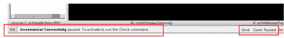
-
Choose File – Check and Save or Check – Current Cellview to run a batch connectivity extraction.
The message clears from the status bar, and the incremental status changes from Paused to On.

Cellviews Ignored by Incremental Connectivity Extraction
The schematic connectivity extractor ignores schematic Pcell supermasters and submasters. This is because a schematic Pcell can create internal connectivity that does not match its representation on the canvas. For example, a Pcell might directly connect instance terminals and terminals to nets without any of the corresponding graphical wires and pins. Extracting this connectivity in a way that matches the canvas representation risks overwriting the intended result.
The extractor also ignores schematics where the schType property is set to noSchEdit. This property indicates that a schematic should not be processed by the schematic checker, geometry management system, and so on and is useful for generated schematics with special or incomplete connectivity or graphics.
Understanding when Incremental Connectivity Extraction Runs
This section describes how incremental connectivity extraction behaves when you are running Virtuoso in non-graphical mode, for example, by using the SKILL interface or by launching Virtuoso with the -replay option.
Incremental Connectivity Extraction and SKILL
Incremental connectivity extractions run when Virtuoso becomes idle after finishing each top-level SKILL command. For example, if you have a SKILL procedure that builds a schematic:
// create.il
procedure(createSchematic()
...build a schematic using various SKILL functions...
schCheck(cv)
cv
)
And you run the following SKILL command:
load("create.il")
sch = createSchematic()
In this case, incremental connectivity extraction runs only after the sch = createSchematic() line finishes. It does not run after each individual command inside createSchematic(). Additionally, incremental connectivity extraction only runs if there is something to extract. Because createSchematic() ends with a call to schCheck(), no further extraction is required. To update connectivity inside a SKILL procedure, call schCheck() explicitly.
Incremental Connectivity Extraction and Replay Files
If you have a replay file containing individual editing commands, for example:
// replay.il
\i schHiCreateInst()
...
\i schHiCreateWire()
...
And you run the following command:
virtuoso -replay replay.il
In this case, incremental connectivity extraction runs after each line, because all lines are considered to be top-level commands.
Connectivity with Objects
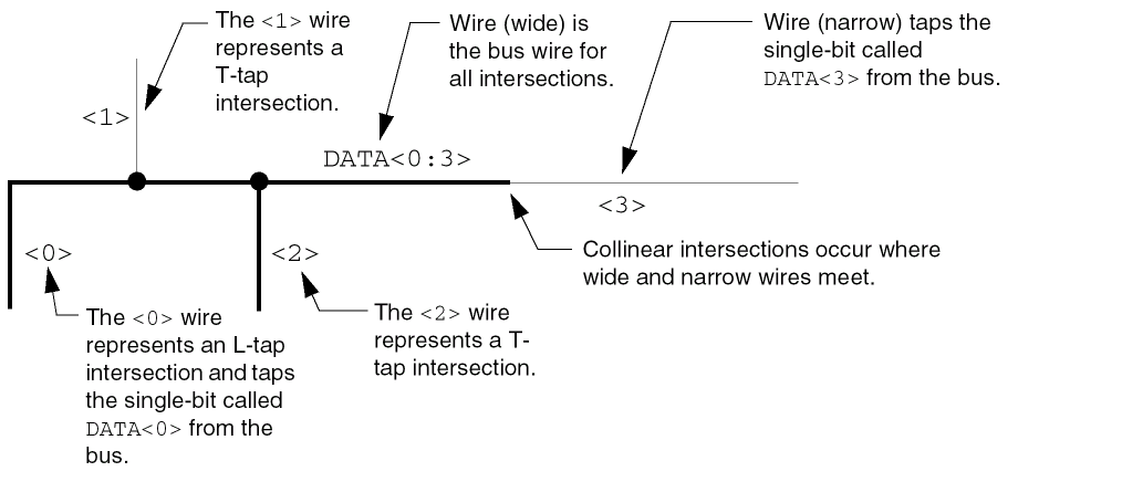
Connectivity is the logical connection between signals in a design. Connectivity is derived (extracted) from the physical connections found in a schematic. Pins and wires implement physical connections. Terminals and signals implement logical connections. Pins and terminals indicate which signals in a cellview are imported from or exported to other levels of a design hierarchy.
A complete schematic design provides input data for a variety of design tools, such as simulation and layout. It is essential, therefore, that you establish connectivity in your schematic designs. The following diagram shows connectivity and naming conventions.
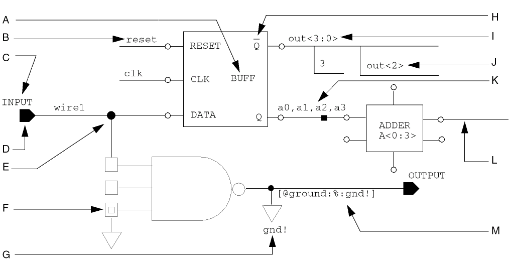
| Key | Connectivity / Name | Key | Connectivity / Name |
|---|---|---|---|
Instance Naming Conventions
You can name instances using any one of the following naming conventions:
Related Topics
System-Generated Names
If you do not name an instance explicitly, the schematic editor assigns a default instance names by using I plus a number. The schematic editor automatically increments the instance number starting from 0.
The advantage of system-generated instance names is that you never have to type a name on the Add Instance form. You can add many instances very quickly and automatically.
You can also change the instance name prefix ( I ) to another letter. For more details, see Changing the Default Instance Name Prefix.
User-Defined Names
The advantage of user-defined names is that you can explicitly name instances in your design. Examples of user-defined names are as follows:
A0 A1 A2 A3
ABC DEF HIJ
IOLATCH FLIPFLOP
Each user-defined name you add must be a string of one or more characters. You must name an instance when you create it using the Add Instance form. If you do not name the instance explicitly, the system generates a name for you.
On the Add Instance form, separate each instance name by a space; for example, ABC BCD.
Related Topics
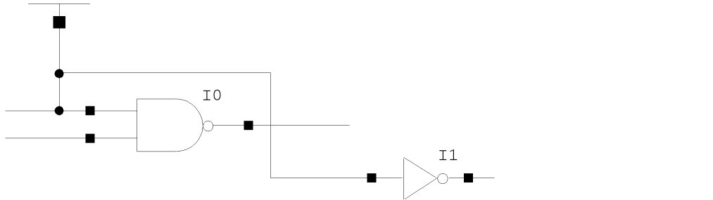
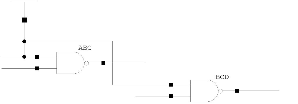
Iterated Names
An iterated name is a compact way to describe many similar instances. This is useful in bus-type or data flow architectures that have identical structures to handle each bit on the bus. It also saves space in your design.
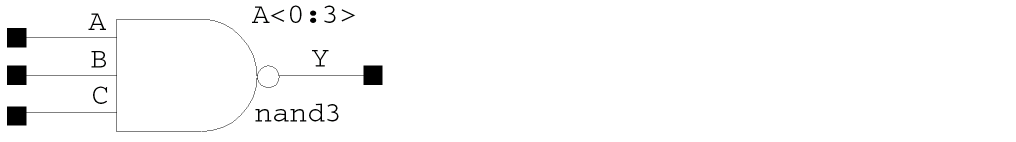
This example uses the base name A. The 0 to the left of the colon and the 3 to the right of the colon indicate the numbered range (0 through 3), which names instances A<0>, A<1>, A<2>, and A<3>.
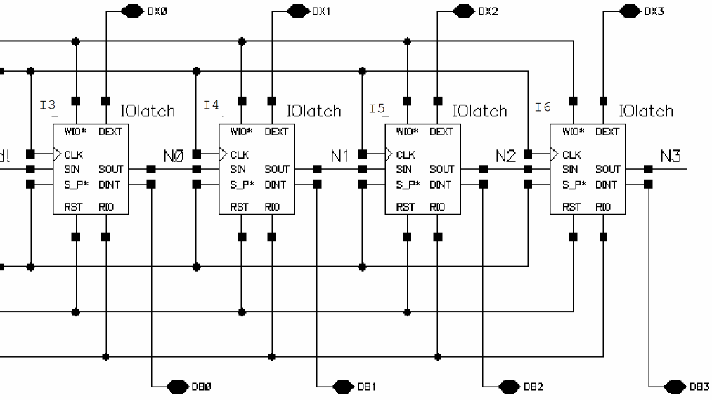
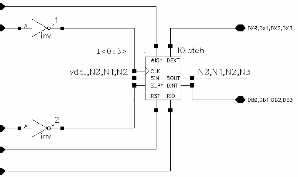
Iterated instances save space. The instances in the following two figures represent identical circuitry, but the second figure is easier and faster to create.
The first schematic shows four IOlatch instances in a design: I3, I4, I5, I6. Compare this with the next schematic.
This schematic shows one IOlatch iterated four times: I<0:3>. Compare this with the previous schematic.
Wire Connections and Wire Naming Conventions
You can connect single-bit wires in your design using any one of the following conventions:
- Wire-to-Wire Connections
- Wire-to-Pin Connections
- Wire-by-Name Connections
- Wire-to-Iterated Instance Connections
-
Global Net Name Connections
- As you move the pointer over another wire or near a pin while you draw the wire, a small diamond appears to show you the nearest object with which you can establish electrical connectivity.
-
Press
sto snap the wire to the nearest object that shows a diamond shape. - You can zoom in on your design to see if you are making an accurate connection.
Wire-to-Wire Connections
If you draw two intersecting wires in a T configuration, the schematic editor automatically connects the wires.
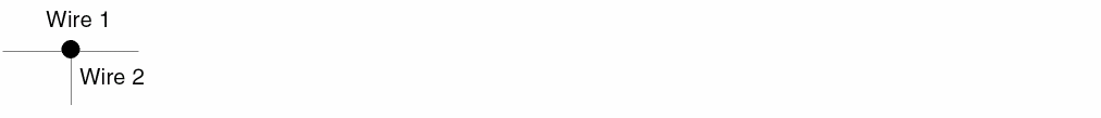
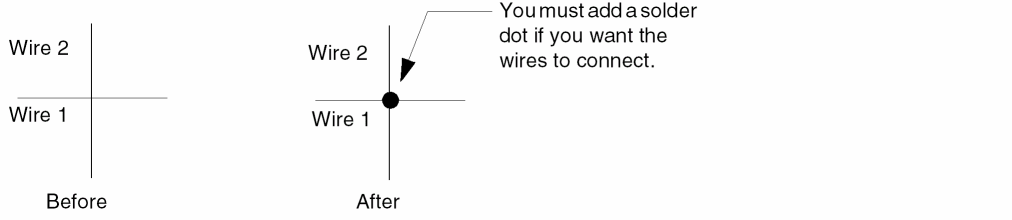
If you draw two wires that cross, you must explicitly add a solder dot to make the connection at the crossover.
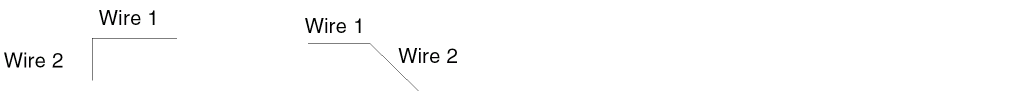
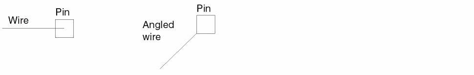
If you draw two (right-angle) wires in an L configuration, or if you draw an angled wire and a wire that intersect at their end points, the wires are connected, but the schematic editor does not add a solder dot.
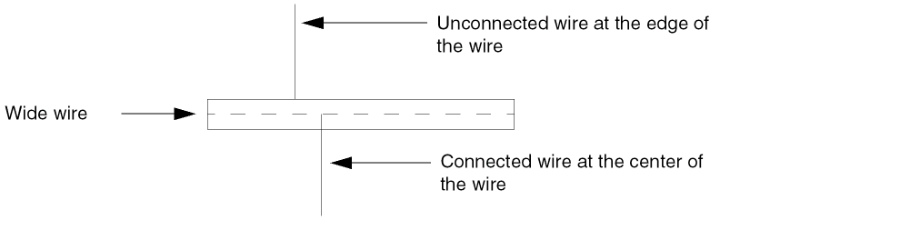
If you connect a narrow wire to a wide wire (for example, in a bus), try to intersect the centerline of the wide wire.
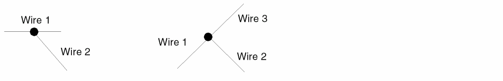
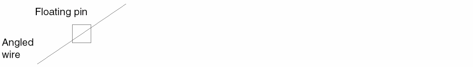
If you want to connect to an angled wire, you must connect to one of its endpoints. The schematic editor automatically adds a solder dot after you add the last wire in each of these examples.
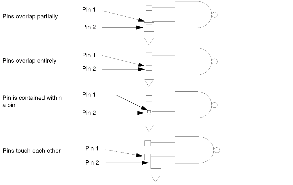
Wire-to-Pin Connections
To make wire-to-pin connections, the wire must intersect the pin.
-
Draw the wire so it ends in the body of a pin.
-
Draw the wire so it ends on the border or perimeter of a pin.

-
Draw the wire so it passes through a pin.

-
You cannot make a wire-to-pin connection by drawing an angled wire that passes through a pin.
Wire-by-Name Connections
A signal is said to be “connected by name” if more than one physically disjoint wire or group of wires exist that carry the signal.
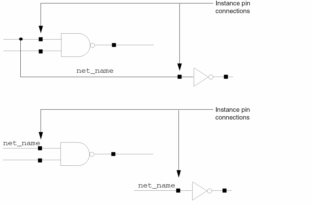
To connect instance pins, assign the same name to each wire. The wires do not have to be physically connected. The system recognizes when a wire and pin have identical names and connects them by name. For example, a wire labeled P connects by name to a schematic pin named P. If you use a local net name, you can connect by name on the same page. If you use a global net name, you can connect by name across all levels of the hierarchy.
When a wire and pin are connected but have different names, the net will take the name of the wire. For example, when a wire labeled x is connected to a pin named P, the pin is placed on a net named x.
You can use the Route Named Connection form to physically connect disjoint wires with the same name.
Be careful not to inadvertently connect a signal across a schematic by using the same name. You can catch this error before your design has been netlisted by checking your design. For more details, see the Instance/Net Name Collision and Pin/Net Name Collision checks on the Schematic Rules Checks Setup form.
Related Topics
Wire-to-Iterated Instance Connections
Before the schematic editor lets you connect a wire to an instance, it checks to see that the net width or pin width equals one of the following:
- Net Width Equal to the Connection Width
- Net Width Equal to the Pin Width
- Net Width Equal to 1
- Pin Width Equal to 1
If the connection cannot be made, an error message is generated when you check your design.
By default, if you do not specify a net name, the connection width will be equal to the net width. This means that the connection width will be the product of the instance width by the pin width. To set the connection width differently, you must add a wire label to the net or schematic pin. The width of this wire label is used unless a width incompatibility error is generated.
Related Topics
Net Width Equal to the Connection Width
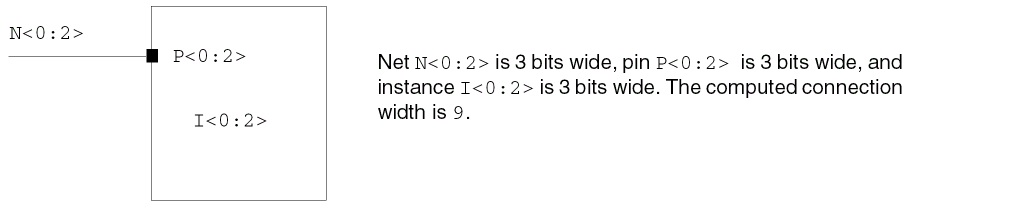
If the net width is equal to the connection width, the schematic editor allows the connection without modifying the design. To determine whether net width equals connection width, the editor compares the net width to a computed connection width. The connection width is computed as follows:
instanceIterationWidth*instancePinWidth
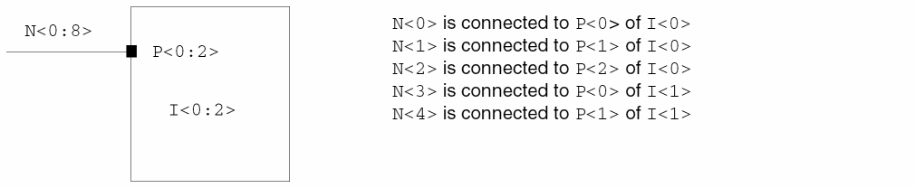
In the following example, the width of instance I<0:2> is 3 and the width of pin P<0:2> is 3. The computed connection width equals 9. The net width N<0:8> also equals 9. Therefore, the connection can be made.
Net Width Equal to the Pin Width
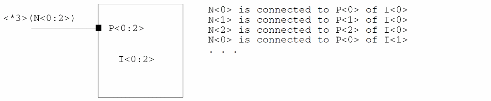
If the net width is equal to the pin width, the schematic editor adds a <*n> to the net width before it allows the connection. If the net width equals the pin width but does not equal the connection width, the editor computes a net prefix repeat operator that equals the instance iterations.
The net width (3) equals the pin width but does not equal the connection width (9). Therefore, the schematic editor generates a net prefix repeat operator, <*3>, for the net in order to allow the connection.
Net Width Equal to 1
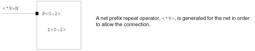
If the net width is equal to 1, the schematic editor adds a net prefix repeat operator to the net width before it allows the connection. If the connection width is 1, the schematic editor computes a net prefix repeat operator that equals the computed connection width.
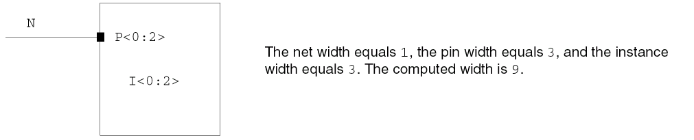
The net width does not equal either the connection width (9) or the pin width (3), but it does equal 1.
Pin Width Equal to 1
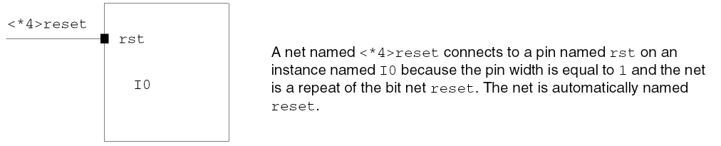
If the pin width is equal to 1, and the net repeats a single bit, the schematic editor connects the pin to the net by extracting its repeating element.
Global Net Name Connections
Global nets make connections across the design hierarchy without using pins and wires to explicitly pass the signal through the hierarchy. Global nets are used primarily for power and ground connections.
To create a global net, add an exclamation mark to the net name.
To make a bus global, add an exclamation mark to the base name of the bus.
Another way to make a net global is to connect it to a pin or instance pin that is global. The net inherits the name of the global pin or instance pin. The basic library has various global symbols you can use to indicate global nets.

gnd!,net3, a separate net gnd! is automatically created for the global part.In summary, you can create a global signal by
- Using the Create – Wire Name command
- Using the Create – Instance command of normal power and ground symbols
Creating a net expression works in a similar way.
Related topics
Multiple-Bit Wire Connections and Naming Conventions
A multiple-bit wire name can be a bundle, a bus, or a combination of the two.
This section describes the following information about multiple-bit wire connections and naming conventions:
Multiple-Bit Wire Naming Conventions
A bus is a wire or pin sharing a common base name. A bus is represented by the base name followed with a vector expression; for example, A<0:7>.
A bundle is a wire or pin name consisting of simple names separated by commas; for example, A,B,Data<0:15>. Spaces are not allowed after the commas. The signals of a bundle do not have the same base name.
You can connect multiple-bit wires in your design using any of the following naming conventions:
- Using Vector Expressions in Multiple-Bit Wire Names
- Using Vector Expressions in Multiple Signals
- Evaluating Vector Expressions in Multiple-Bit Wire Names
- Using Prefix Repeat Operators in Multiple-Bit Wire Names
- Using Suffix Repeat Operators in Multiple-Bit Wire Names
Using Vector Expressions in Multiple-Bit Wire Names
A multiple-bit wire name can be a bundle, a bus, or a combination of the two. You can improve readability in your designs by shortening multiple-bit wire names.
To indicate that multiple bits of one wire carry similar information, give each bit the same base name. Then add a suffix to each bit name to distinguish the signals.
For example, to show four bits of a wire with a common base name (DATA), but with individual suffixes (<0>, <1>, <2>, and <3>), assign the following names: DATA<0>, DATA<1>, DATA<2>, and DATA<3>.
Using Vector Expressions in Multiple Signals
To name a wire that contains multiple signals with the same base name, specify the base name followed by a vector expression. The vector expression can be
-
A list of the individual bit numbers separated by commas and enclosed with angle brackets.
For example,DATA<2,1,0>representsDATA<2>,DATA<1>, andDATA<0>. -
A range of numbers containing a lower and upper bound and, optionally, an increment value. The numbers are separated with colons and enclosed with angle brackets.
For example,DATA<1:7:2>represents
Use a positive integer for incrValue. If you do not specify an increment value, the editor uses 1.baseName<lowerBound:upperBound: [incrValue]>
The ordering of the bits in a bus is important when you are connecting the bus to a pin that has a width greater than 1.
Evaluating Vector Expressions in Multiple-Bit Wire Names
The schematic editor evaluates vector expressions in multiple-bit wire names as follows:
-
The vector expression
DATA<0:3:2>names a 2-bit bus containingDATA<0>andDATA<2>. -
The vector expression
DATA<1:3:2>names a 2-bit bus containingDATA<1>andDATA<3>. -
The vector expressions
DATA<0:3>andDATA<0:3:1>are equivalent names that generate a 4-bit bus containingDATA<0>,DATA<1>,DATA<2>, andDATA<3>.
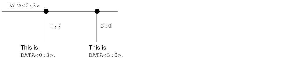
If the lower bound is larger than the upper bound, the schematic editor generates the bit numbers in descending order, as follows:
Using Prefix Repeat Operators in Multiple-Bit Wire Names
You can repeat a single signal name, a group of signal names, or a vector name any number of times in the wire name by placing a prefix repeat operator <*n> in front of the name, where n is a positive integer that defines the number of times to repeat each bit in the vector name.
-
Use the prefix repeat operator
<*n>to repeat a single-signal name. The following equivalent wire names both name the same four-bit wire:<*2>A,B,C A,A,B,C
-
Use the prefix repeat operator <*n> and parentheses to repeat a group of signal names. The following two wire names are equivalent:
<*2>(A,B),C
A,B,A,B,C
-
Use combinations of the prefix repeat operator
<*n>and parentheses to nest parenthetical expressions to any required depth. The schematic editor expands nested expressions from the innermost expression outward. For example, a name with the expression<*2>(A,<*2>(X,Y)),Bexpands toA,X,Y,X,Y,A,X,Y,X,Y,B.
Using Suffix Repeat Operators in Multiple-Bit Wire Names
A suffix repeat operator is a number, <*n>, after a vector name, where n is a positive integer that defines the number of times to repeat each bit in the vector name.
-
Use the suffix repeat operator
<*n>to repeat each bit in a group of bit names before expanding the vector name. For example, the following three names all describe the same six-bit wire:A<0:2*2> A<0*2,1*2,2*2> A<0,0,1,1,2,2>
-
Use the suffix repeat operator
<*n>and parentheses to repeat the sequence of bit names. In this case, the vector name is expanded before the bits are repeated. The following names all describe the same six-bit wire:A<(0:2)*2> A<0:2,0:2> A<0,1,2,0,1,2>
Bus Tapping
Tapping extracts specified bits from a named net and propagates the bits along the design. Tapping a subset of signals from a bus or a bundle is called bus tapping.
You can connect multiple-bit wires in your design using any one of the following naming conventions:
- Tapping Multiple Bits of a Bus
- Tapping Multiple Bits of a Bundle
- Tapping Wire Intersections by Name
- Designating Tap Size and Bit Order
- System-Generated Net Names
To create a bus tap
-
Connect a wire that carries the subset of signals to the bus or bundle that contains the signals.
You can use one of the many different configurations of wire-to-wire or pin-to-wire connections to create the bus tap. -
Add the name of the bus tap that specifies the tapped signals.
The name depends on whether you tap from a bus or from a bundle.
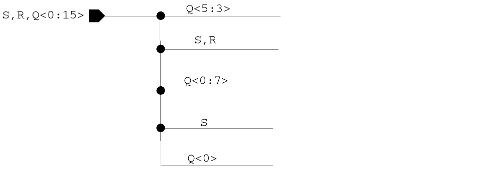
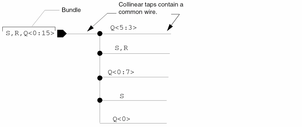
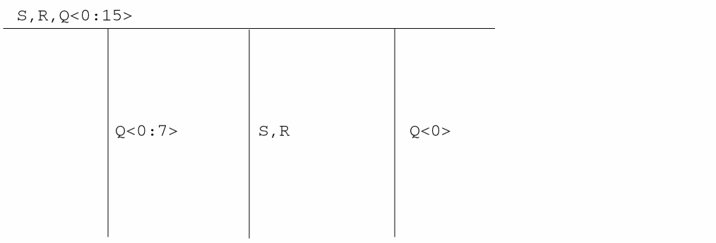
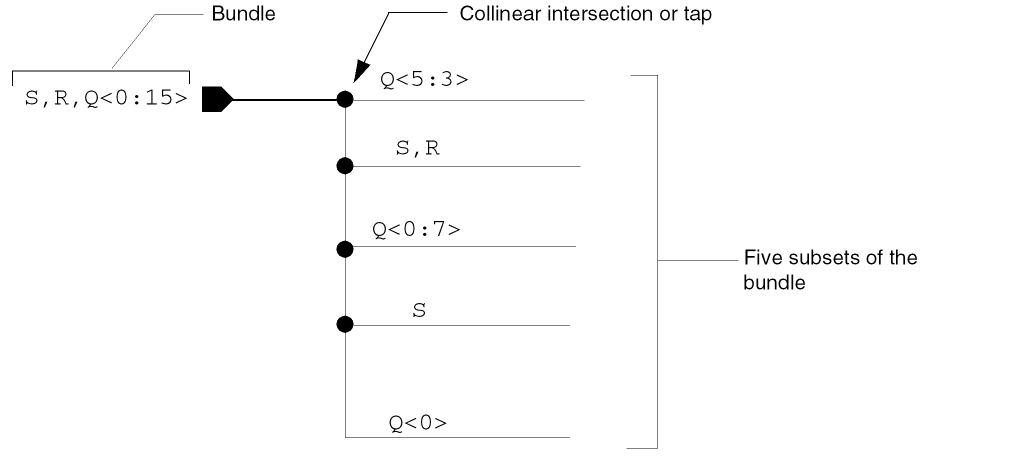
Tapping bits of a bus or bundle gives the tapping wire segments names that are members of the base bus or bundle. For example, in the following illustration, all names on the right are taps from the bundleS,R,Q<0:15>.
Tapping Multiple Bits of a Bus
In the previous section, it explains how to tap a wire from a bus. A wire that taps a bus, can itself also be tapped by using
To improve readability in your design, rather than repeating the base name of the bus for each tapped wire, you can just name each wire using the vector expression. Any wires or pins of instances connected to tap wires receive the name of the tapped signal. This process is called “cascading” bus taps. If a tap wire carries more than one bit from the bus, the schematic editor can tap that wire.
The previous example, would look like this:
3 is connected to a bus that contains the same number within its base name D<2:5>, the wire is recognized as a tap. If there is not a bus to connect to, the same wire is recognized as a net.
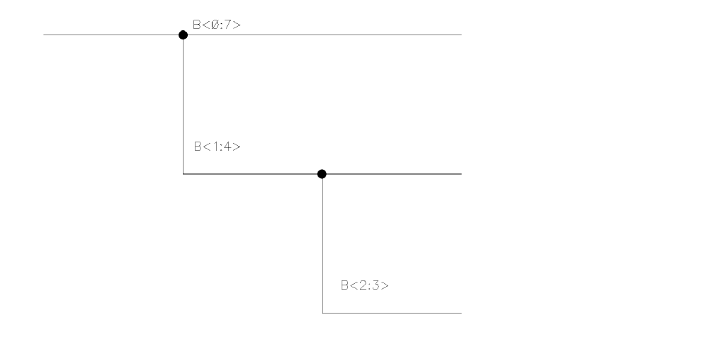
You can create a geometric configuration when a tap wire carries more than one bit from the bus. The single-bit taps <0>, <1>, <2>, and <3> are drawn from the two-bit taps <0:1>, <2:3> rather than directly from the DATA<0:3> bus.
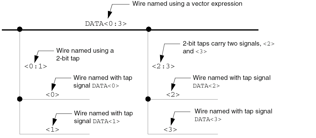
As shown in the above example, if you intersect a bus wire named DATA<0:7> with a tap wire named <0:3>, you can intersect the tap wire with a second tap wire named <0:1>. The name of the first tap wire becomes DATA<0:3>. The name of the second tap wire becomes DATA<0:1>.
You can also intersect the second tap wire with other tap wires to individually tap bit <0>, bit <1>, and so on. In general, you can intersect any bus with a tap wire, even if the bus itself is a tap of a larger bus. Taps can cascade down any number of steps.
Tapping Multiple Bits of a Bundle
You tap bits of a bundle when you connect wires to a bundle and name the wires accordingly. For example, in the following illustration, all multiple-bit wires use signal S, signal R, or bus Q.
You can also use enclosed names to tap from a bundle. For example, <S,R> can be used to tap from the bundle S,R,Q<0:15>. However, <S,R> cannot be used to name a wire by itself.
To tap signals from a bundle (that is, a multiple-bit wire with signals that do not have the same base name), you must specify the basename of the signals in the wire name to indicate numbered bits.
In the following example, bus Q<0:7> taps eight bits from bus Q<0:15>, which is part of a bundle. In this case, the tap name contains a base name with a S,R taps two signals with different names from the bundle. In this case, the wire name is a list of names separated by commas.
The following example shows the same multiple bits of a bundle with a pin and a collinear intersection or tap.
Like with buses, you can intersect any bundle with a tap wire, even if the bundle itself is a tap of a larger bundle. Taps can cascade down any number of steps.
Tapping Wire Intersections by Name
The following illustration summarizes how to specify bus tap intersections.
Any other wires or pins of instances connected to tap wires receive the name of the tapped signal. This process is called “cascading” bus taps. Any narrow or wide wire connected to the wire named <3> is connected to the DATA<3> bit of the bus. Any wire connected to the wire named <2> is connected to the DATA<2> bit of the bus, and so on.
Designating Tap Size and Bit Order
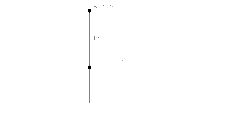
A tap wire from a bus can contain any number of bits with the constraint that each bit must appear somewhere in the bus. This can be achieved with or without repeat operators in the tap expression. For example, you can intersect a 4-bit bus wire named A<0:3> with an 8-bit tap wire named <0:1*2,(0:1)*2>. The resulting name of the tap wire is A<0,0,1,1,0,1,0,1>. Alternatively, you can intersect a bus named A<2:0> with a tap wire named A<0>,A<0>,A<0>.
The schematic editor orders bits in a bus just as they appear in the bus name. Similarly, the editor orders bits in a tap as they appear in the tap name.
For example, you can tap the four bits of a bus named DATA<0:3> in order from DATA<0> to DATA<3>. However, a tap wire named DATA<3:0> that intersects with bus DATA<0:3> taps the bits in reverse order, as shown in the following figure.
System-Generated Net Names
Tapping starts from the bus or bundle with the largest number of unique bits, and cascades outward from there.
Any unnamed wire segments that intersect are grouped and placed onto the same unnamed net. The named nets that intersect with this net are used to derive a system generated name.
The following items explain how the system determines a name for unnamed wire segments.
- The schematic editor places all unnamed intersecting wires in the same unnamed net.
- To determine the name of the unnamed net, the schematic editor chooses a name from among the named nets that intersect with the unnamed net. Named nets are those nets whose names are derived from wire names, schematic pins, or tap names.
-
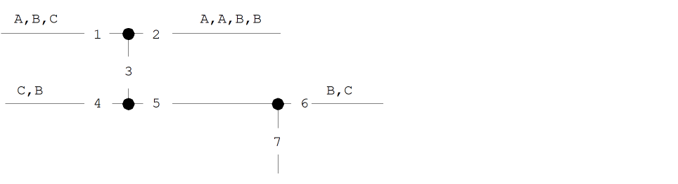
The chosen name for the unnamed net is the one with the largest number of unique members. For example, a net named
A,B,Chas three unique members, but a net namedA,Ahas only one unique member. - At all wire-wire and wire-pin intersections, the schematic editor verifies that all names present at the intersection are members of the name that contains the most unique members.
For example, in the following illustration
-
The schematic editor places wire segments
3,5, and7in the same net because these segments are intersecting and unnamed -
This unnamed net is then named
A,B,Cbecause it takes the names of all the intersecting named nets. The nameA,B,Cis the one with the most unique member names; that is, three. -
The schematic editor then verifies that all intersecting named nets (
B,C,C,BandA,A,B,B) are taps ofA,B,C.
Pin Connections and Pin Naming Conventions
You can name pins in a design to declare which nets in the schematic are connected to a higher level of the design hierarchy or which nets span across sheets in a multisheet schematic.
Each pin name must be unique and observe the
This section describes the following pin connections and naming conventions:
Hierarchical and Offsheet Pin Names
If you are designing a multisheet schematic, your sheets contain hierarchical pins and offsheet pins.
Hierarchical pins are pins that also appear on the symbol of the design. The hierarchical pins from each sheet become the hierarchical pins of the multisheet. Each hierarchical pin in a multisheet design must have a unique name.
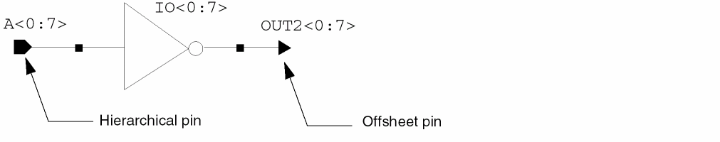
Offsheet pins connect signals across the sheets of a multisheet schematic only. Use the same name for the offsheet pins on each sheet.
If you want a signal to appear on a multiple sheet that is also exported by a hierarchical pin, place a hierarchical pin for the first usage and offsheet pins on the other sheets.
Bus Pin Names
Use a IN<16:10:2> expands to these four pins: IN<16>, IN<14>, IN<12>, and IN<10>.
Pin-to-Pin Connections
A direct connection between two instance pins without an intermediate wire is called a pin-to-pin connection. There are four ways to make pin-to-pin connections:
Tapping Pins
Tapping pins is similar to
If a schematic pin has a bus name, you can draw a tap directly from the pin using a
The following figure shows how to tap pins in a design.
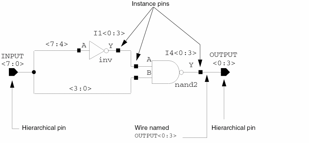
In the example above, the wire named <7:4> is a tap of the schematic pin named INPUT<7:0> and connects a four-bit bus called INPUT<7:4> to the input of the inverter (a four-bit iterated instance).
The wire named <3:0> is also a tap of the INPUT<7:0> pin and connects a four-bit bus called INPUT<3:0> to the input of the four-bit nand2 gate.
If you do not apply a name to a net that is attached to a pin, the schematic editor gives the net the same name as the pin. For example, the wire that connects the output of the nand2 gate to the OUTPUT<0:3> pin is called OUTPUT<0:3>.
Patch Cord Connections and Patch Cord Naming Conventions
A patch cord is a special connection symbol. You can use a patch cord to:
- establish aliases between the signals of two different nets
- copy one net to another (this is different to tap names, where you extract bits of a single net)
- map bits from one net to different bits of another net
- connect multiple nets (merge two buses)
The value (connection expression) of the src (source) pin to the bits of the net attached to the dst (destination) pin.
The syntax you use for naming the src vector expression must equal the number of bits in the dst vector expression.
Related Topics
Adding Patch Cords Using the Add Instances Form
Adding Patch Cords Using the Create Patchcord Form
Naming Single and Multiple Bits Using Patch Cords
The schPatchExpr connection expression (value) for patch cords has the following form:
srcVectorExpression = dstVectorExpression
where srcVectorExpression is the source and dstVectorExpression is the destination.
Naming conventions for patch cords using
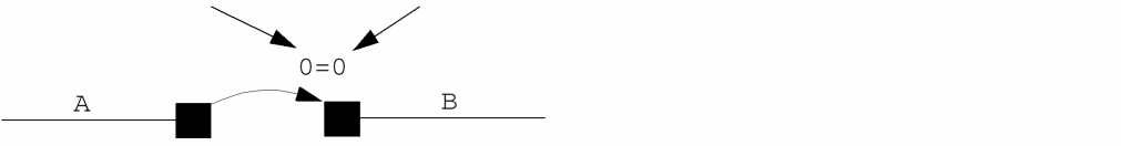
In the following example, nets A and B are aliased together. Logically, each object that A is connected to is also connected to B, and the patch cord connects the first bit named in srcVectorExpression to the first bit named in dstVectorExpression.
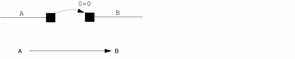
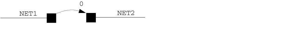
If you want to connect two single-bit nets called NET1 and NET2 with a patch cord, a connection expression of 0 is sufficient:
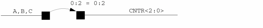
In the following example, signal A is aliased to CNTR<2>, signal B is aliased to CNTR<1>, and signal C is aliased to CNTR<0>.
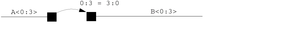
In the following example, A<0> is aliased to B<3>, A<1> is aliased to B<2>, A<2> is aliased to B<1>, and A<3> is aliased to B<0>.
Naming Multiple Nets Using Patch Cords
The following figure shows how to use patch cords to merge two buses.
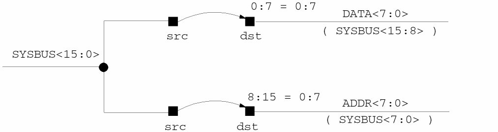
The upper patch cord connects the eight-bit bus SYSBUS<15:8> to the eight-bit bus DATA<7:0>. The lower patch cord connects the eight-bit bus SYSBUS<7:0> to the eight-bit bus ADDR<7:0>.
The range of bits named in the lower patch cord using srcVectorExpression <8:15> does not refer to the bits of SYSBUS. It refers to the order of the bits attached to the src pin of the patch cord. Therefore, according to the connection expression, bits 8 through 15 of bus SYSBUS<15:0> (corresponding to the bits named SYSBUS<7:0>) are connected to bit 0 through 7 of bus ADDR<7:0> (corresponding to the bits named ADDR<7:0>).
Inherited Connections
If you have a need to change the value of a global signal in your design, you can do so without recreating a complete hierarchical branch. You can build one library containing components potentially requiring different power and ground connections in different parts of a design. This is referred to as an inherited connection.
Inherited connections let you selectively override global signals in designs originated in the Virtuoso® Schematic Editor. To have this override information available to other Cadence® tools across the design flow, the override information is communicated to the software by means of net expressions and a class of properties called netSet properties.
Inherited connections is an extension to the connectivity model that allows you to create special global signals and override their names for selected branches of the design hierarchy. This flexibility allows you to use
- Multiple power supplies in a design
- Overridable substrate connections
- Parameterized power and ground symbols
The inherited connections feature is recognized by many tools throughout the IC design flow.
This section describes the following information about inherited connections:
- Inherited Connections in a Hierarchy
- Defining Inherited Connections
- The Syntax of an Inherited Net Expression
- How Net Expressions Evaluate
- Sample Net Expression Library
- Inherited Connections Restrictions
Inherited Connections in a Hierarchy
You use inherited connections to selectively override global signals within your design. Consider the following example and explanation:
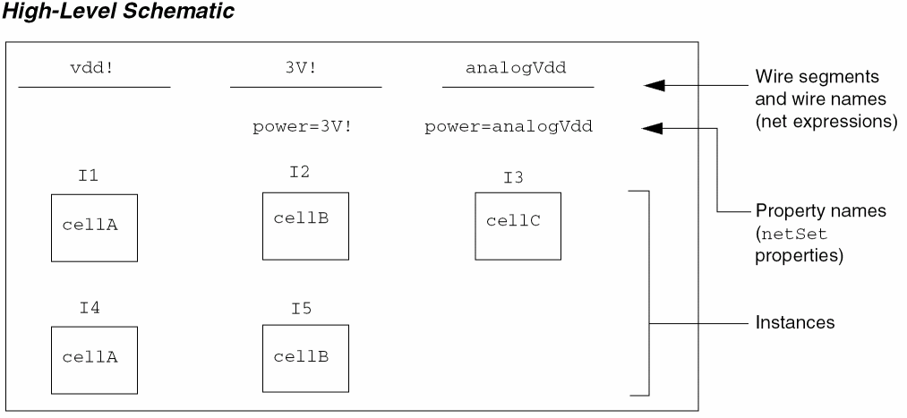
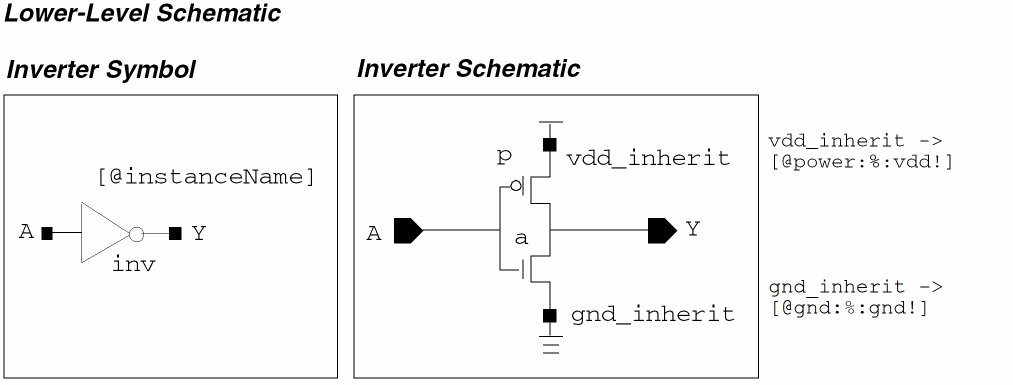
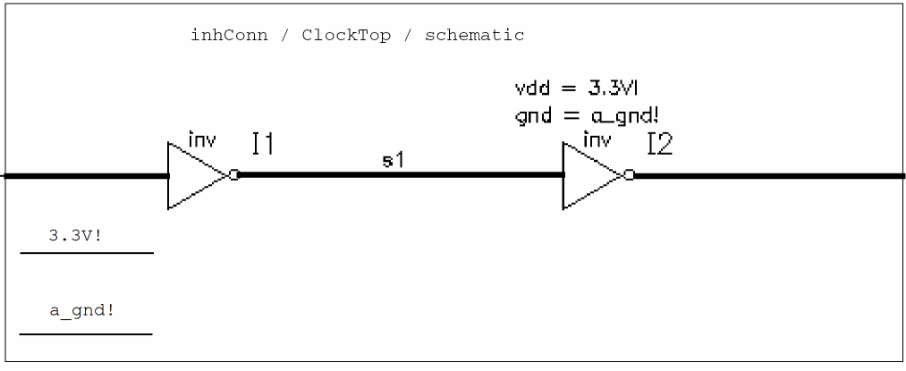
The high-level schematic shows five instances: I1, I2, I3, I4, and I5. Each instance represents a portion of the design, each of which eventually references the inverter shown in the lower-level schematic.
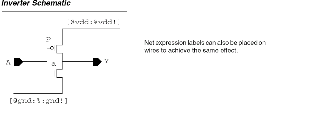
In the inverter schematic, the power and ground wires are defined using the net expressions [@power:%:vdd!] and [@gnd:%:gnd!], respectively. By default, all inverter pmos transistors are connected to vdd! and all nmos transistors are connected to gnd!.
In the high-level schematic, all the inverter pmos transistors below instance I2 of cellB are to use 3V! as the power supply, and the inverters in instance I3 of cellC are to use analogVdd.
To selectively override the default global signal vdd!, create a netSet property on instance I2 named power with the value 3V! and a netSet property on instance I3 named power with the value analogVdd. Notice that the inverter pmos transistors below instances I1, I4, and I5 are still connected to vdd!.
In other words, you place a netSet property on an instance representing the branch of hierarchy where it is to be applied. You can create the netSet property on any instances at any level above the cellviews with net expressions. For example, if a large hierarchical design has seven levels of hierarchy, you can place a netSet property power = 3V! on an I2 instance in the top-level schematic. This affects all the logic below instance I2 all the way to the bottom in all cellviews that contain a net expression, such as [@power:%:vdd!]. All cellviews that contain this net expression would use 3V! instead of vdd! for that branch of the design.
However, if on a lower-level cellview there was an I7 instance with a netSet property power = 2V!, then 2V! would always be used below the I7 instance.
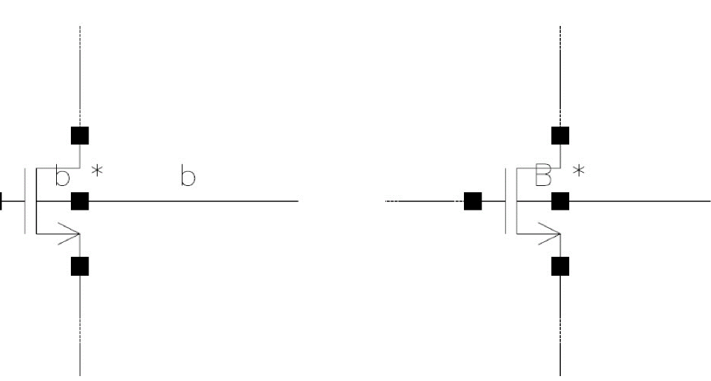
Using Physical Connections to Override Inherited Instance Pins
You can override an inherited instance pin by connecting a labeled wire or a schematic pin. For example, in the below-mentioned design, the wire labeled b overrides a [@BULK:%:gnd!] net expression on the left instance's bulk terminal. Pin B overrides the right instance's bulk pin net expression.
Defining Inherited Connections
In the schematic editor, you define an inherited connection by adding a net expression label to either a wire or a pin. A net expression defines the default global signal name for the connection and the name of a property that can be used to override that default global signal name.
The Syntax of an Inherited Net Expression
The syntax of an inherited net expression is a subset of that of an NLP (Natural Language Processing) expression. The four components are the search scope, search property name, format instruction, and default global signal name.
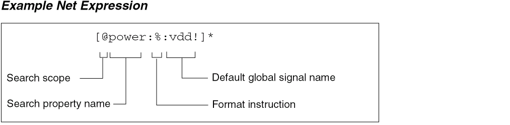
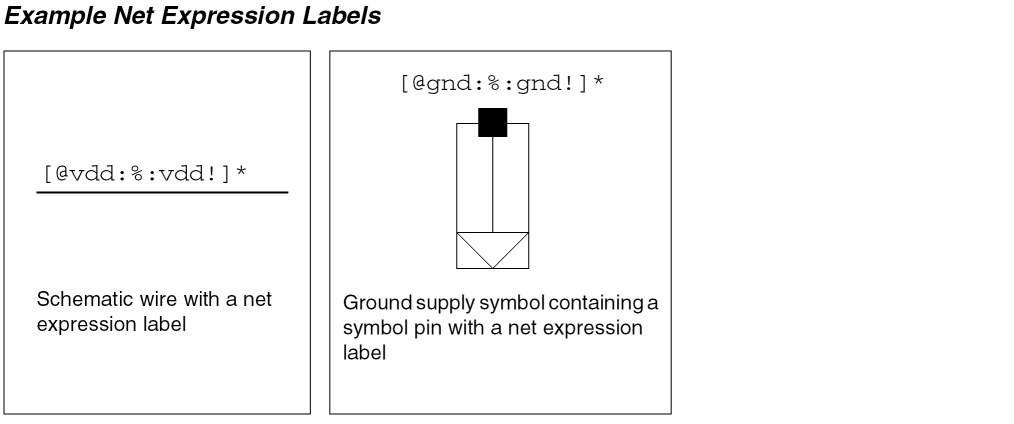
The asterisk ( * ) after a global name shows that this is not a regular wire name but a name that is an overridable net expression. The default global signal name specifies what the wire or pin is connected to by default.
How Net Expressions Evaluate
The search scope is limited to the @ search, which requires an instance lineage. The search travels up the instance hierarchy looking for an instance property of the given search property name until either an override is found or the instance lineage is exhausted. The default signal name must be global in nature and serves two important purposes: it names the net locally and is the inherited signal when no override is found during the search. The format instruction (%) is retained here in compliance with the syntax of an NLP expression.
The lookup property is a netSet type and is used only for an inherited connection. The netSet property value can be one of the two possibilities: an override signal name or an overriding, redirecting net expression. The former is the inherited signal name while the latter case redirects the search to a new property name and may introduce a new default signal name to replace the one in the original net expression in the hierarchy below it. The search for the new lookup property starts with the current instance where the netSet property with the override inherited net expression is found.
Net expressions are evaluated for each hierarchical path. The schematic editor uses the property name specified in the net expression label to search upward from the cellview containing the net expression label (one instance at a time) to the top of the design. The first instance that is found that has a matching property name terminates the search. If the property is of type netSet and is a legal net name, its value is used as the connecting net rather than the default net name specified in the expression.
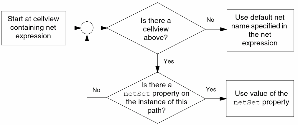
The netSet property can be placed on any instance and it will affect all net expression labels with matching property names at all levels below that instance unless overridden by another netSet property on a lower-level instance.
You can create an inherited connection in a schematic by placing an instance of a symbol where one of the symbol pins has a net expression label. When the extractor runs on the schematic, the net expression label from the symbol pin is propagated onto the net within the schematic.
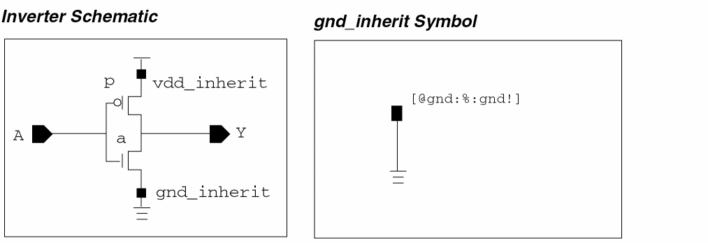
The basic library contains sample parameterized power and ground supply symbols called vcc_inherit, vdd_inherit, gnd_inherit, and vss_inherit.
| Inherited Supply Symbol | Net Expression Label |
|---|---|
Sample Net Expression Library
The location of a sample design that uses inherited connections is
your_install_dir/tools/dfII/samples/tutorial/inhConn/inhConn/schematic
The following design shows the top-level schematic cellview.
Inherited Connections Restrictions
You should be aware of some restrictions when using net expression labels and netSet properties:
- When you are creating a block (or the components of a block) that will be shared, distributed, or used elsewhere, Cadence recommends defining all inherited connections as explicit pins rather than as implicit terminals.
-
The default name in a net expression label must denote a single-bit (scalar), global name. For example,
vdd!andmygnd!are legal;bus!<0:15>andvddare illegal. -
The property you use to override an inherited connection must be of type
netSet. -
The
netSetproperty value must represent an existing single-bit signal name (for example,A,clock, ormyPower!) or another net expression. -
Within one cellview, you cannot use two different net expression labels for the same default global signal. Therefore, using both
[@power:%:vdd!]and[@vdd:%:vdd!]in the same cellview is not allowed.
Related topics
Adding Net Expression Labels to Create an Inherited Connection
Adding netSet Properties to Create an Inherited Connection
Analyzing Net Expression Property Names and Evaluated Names
Summary of Naming Conventions
The following tables detail the naming conventions.
| Character | Symbol | Description | Example |
|
Enclose expressions for multiple-bit wires; used for iterators ( |
|||
| Character | Symbol | Description | Example |
|
Separates a range of numbers expressed by a starting and ending number |
| Character | Symbol |
| Character | Symbol |
| Name | Description |
|
A string of printable ASCII characters that does not include
|
|
|
baseName optionally followed by a { |
|
|
A string consisting of nameTerm, optionally prefixed with the [ < * |
|
|
A single number or a range of numbers. The range can be expressed by a starting, ending, and increment number, separated by colons.
vectTerm can also be a
|
|
|
A single or repeated vectTerm. The optional
|
| Name | Description |
|
A string of printable ASCII characters that does not include
|
|
|
baseName optionally followed by a number or a range of numbers separated by a colon. Single-bit and iterated instance names must be unique. A single-bit name cannot imply more than one member. An iterated instance name must imply the same number of members as iterations.
|
| Sample Name | Members | Expanded Form |
nth member name, use a zero-based counting method to find the nth element in the expanded form. For example, -
Member zero of
<*2>(a,<*2>b)isa -
Member one of
<*2>(a,<*2>b)isb -
Member two of
<*2>(a,<*2>b)isb, and so on
If the name contains a b<0:1,2:2>, then
-
Member zero in this case is called
b<0> -
Member one in this case is called
b<1> -
Member two in this case is called
b<2>
Table 2-7 Expanded Names for Instances
Name Members Expanded Form
Supply and Ground Sensitivity
When a digital net connects to an analog net, the logic value on the digital net requires to be converted to a voltage value on the analog net for simulation. This is reversed when a analog net connects to a digital net, the voltage value on the analog net requires to be converted to a logic value. With multiple supply designs, you need to specify the applicable supply (out of many) to be used for the conversion. You can do this by adding two properties; supplySensitivity and groundSensitivity to the cellview terminals. These properties will subsequently distinguish the power and ground supplies applicable to the net.
Setting Supply and Ground Sensitivity (Schematic Window)
You can specify the supply and ground terminal names that are to be used to make a pin’s terminals sensitive to specified supply terminals. When editing, this allows the sensitivity terminal attributes to be set correctly at the time of creation.
The Create Pin – Schematic and Edit Object Properties – Pin forms have supply sensitivity options with corresponding drop-down fields to select appropriate terminals.
For example, the terminal pin1 could be set so that it would be sensitive to the power terminal vdd and the ground terminal gnd. If there is no pre-established supply sensitivity of the pin’s terminal, then these fields will be left blank. In such cases, you can type in the names of the power and ground terminals, or use the value option to populate the field.
The pin name and the specified power and ground terminals must be single-bit terminals (scalar) or single-bit terminals with vector elements (vector bit). They must pre-exist in the database before the sensitivity relationship is established. If you specify terminals that do not already exist in the database, or if the terminal name is not a single-bit, this will invoke an error condition. Subsequently, no pin placement will take place, the error field will be highlighted, and an error message will be displayed in the CIW.
To set supply and ground sensitivity:
- In the Virtuoso Schematic Editing window, select Create – Pin to display the Create Pin form.
-
Provide a pin name. The pin name should be a single-bit terminal or single-bit terminal with vector elements for a pin to be created with pwr or gnd sensitivity. If the name is not a single-bit, a signal type can only be added if the Expand Busses option is also selected which will apply to the array of pins.
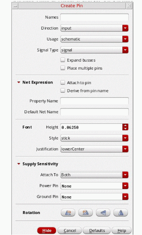
-
Expand Supply Sensitivity to reveal three drop-down lists: Attach To, Power Pin, and Ground Pin.
-
Select the required option from the Attach To drop-down list to apply to the next pin.
For example, if you set Attach To toBoth, Power Pin tovdd, and Ground Pin tognd, the terminals for the next pin (pin1) will be sensitive to the power pinvddand the ground pingnd. Likewise, if you set Attach To toPower,pin1will only be sensitive to the power pinvddeven if there is an entry in the Ground Pin field. -
In the Power Pin field, select from the drop-down list, or type in, the name of the power pin that the next pin is to be sensitive to.
-
In the Ground Pin field, select from the drop-down list, or type in, the name of the ground pin that the next pin is to be sensitive to.
The default is the first or most recently used ground pin. - If required, collapse the Supply Sensitivity section to hide the options you have set.
Related Topics
Create Pin – Schematic (form)
Setting Supply and Ground Sensitivity (Symbol Window)
Editing the Sensitivity Terminals of Schematic and Symbol Pins
Editing the Optical Signal Types
Setting Supply and Ground Sensitivity (Symbol Window)
The behavior of the Create Pin form in the symbol window is as described for the schematic window (see Setting Supply and Ground Sensitivity (Schematic Window), in that you would also expand Supply Sensitivity to expand the Create Pin form.
The specified power and ground terminals must be single-bit terminals and pre-exist in the database before the sensitivity relationship can be established. If you specify terminals that do not already exist in the database, or if the terminal name is not a single-bit, a warning is given and the selection will revert back to the previous choice.
Related Topics
Create Pin – Symbol (form)
Setting Supply and Ground Sensitivity (Schematic Window)
Editing the Sensitivity Terminals of Schematic and Symbol Pins
Editing the Optical Signal Types
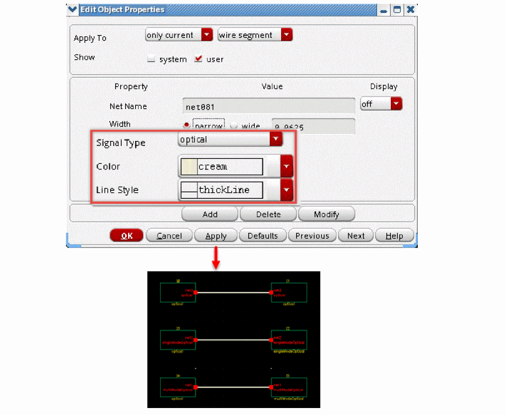
Editing the Sensitivity Terminals of Schematic and Symbol Pins
Use the Edit Object Properties form to edit the sensitivity terminal attributes of the schematic and symbol pins.
-
With the pin to be edited selected, choose Edit – Properties – Objects.
The Edit Object Properties – Pin form appears. -
Select the appropriate terminal for Pwr Sensitivity using the corresponding value drop-down field.The specified power and ground terminals must be single-bit terminals and pre-exist in the database before the sensitivity relationship is established. If you specify terminals that do not already exist in the database, or if the terminal name is not a single-bit, this will invoke an error condition. Subsequently, no pin placement will take place, the error field will be highlighted, and an error message will be displayed in the CIW.
-
Select the appropriate terminal for Gnd Sensitivity using the corresponding value drop-down field.
For example, we could set the terminals forpin1so that it would be sensitive to the power terminalvddand the ground terminalgnd. If there is no pre-established supply sensitivity of the pin’s terminal, then these fields will be left blank. In such a case, you can type in the names of the power and ground terminals, or use the value option to fill the field. - Click OK.
Editing the Optical Signal Types
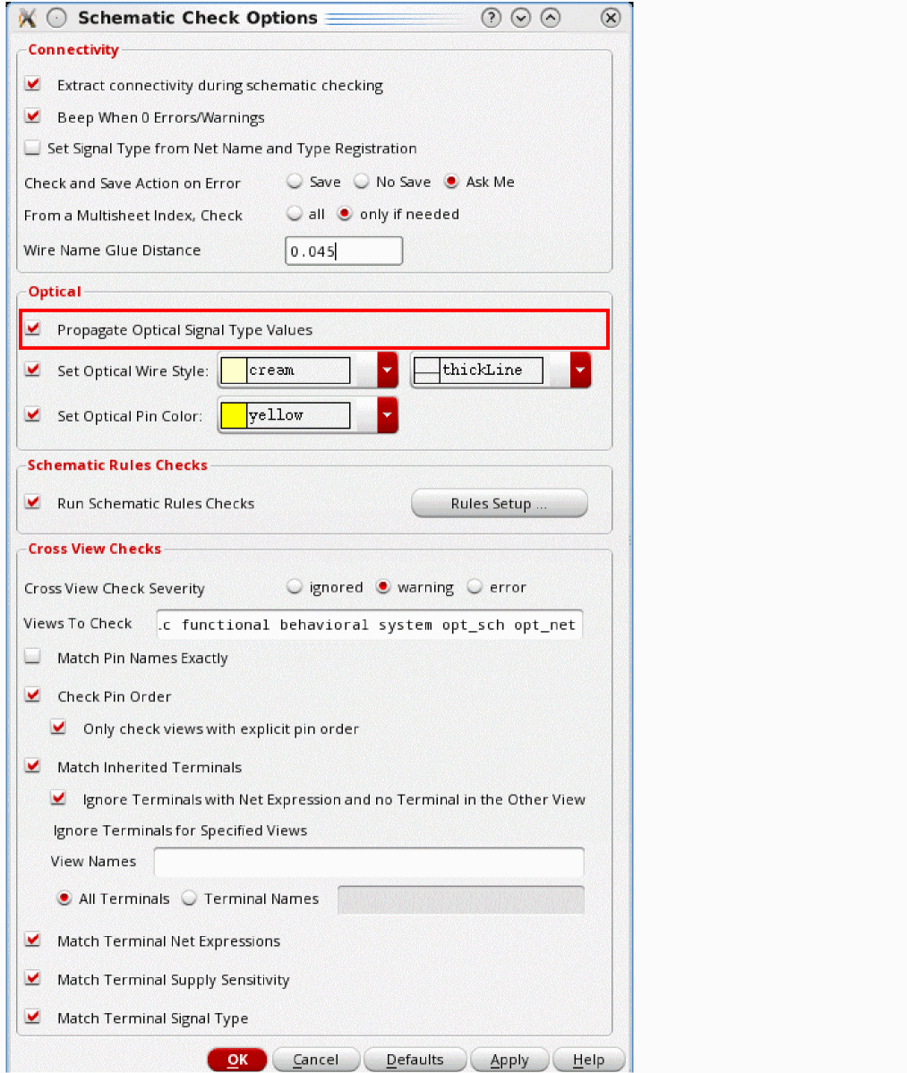
Use the Edit Object Properties – Pin form to view or edit optical signal types optical, singleModeOptical, and multiModeOptical on pins and wires. You can set a distinctive color and line style to identify the optical wires.
Checking Sensitivity Between Schematic and Symbol Cellviews
The sensitivity of a terminal should be consistent between the schematic and symbol cellviews. You can ensure that this consistency is validated by selecting the Match Terminal Supply Sensitivity check box in the Schematic Check Options form (Options – Check). This option is on by default.
Related Topics
Schematic Check Options (form)
Propagating Optical Signal Types (Virtuoso Photonics Option)
The Optical options let you propagate the optical signals and set the optical wire style.
Optical signal types are propagated from an instTerm to a net when the signal type of the net has been specified as optical and has only optical connections. A net that already has an optical signal type is not changed.
For matching optical connections, the common optical signal type is used. Mixed optical connections are resolved by using the specific signal types.
optical + singleModeOptical => singleModeOptical
optical + multiModeOptical => multiModeOptical
A single + multi connection remains unchanged and is processed by the checker.
Environment Variable: opticalSigTypePropagation
You can disable the optical signal type propagation by clearing the Propagate Optical Signal Type Values check box. For more information about the other options on the Schematic Check Options form, see Schematic Check Options.
Equivalent Connectivity Time
You can avoid the need to re-run schematic Check and Save or netlisting if a cellview has equivalent connectivity to the previous version. Before updating a symbol, check the Equivalent Connectivity Time to ensure that it is less than or equal to the time set with the lastSchematicExtraction timestamp property.
You can use the following SKILL functions to specify Equivalent Connectivity Time information in a cellview:
- dbCellViewHasEquivalentConnectivityTime
- dbGetCellViewEquivalentConnectivityTime
- dbSetCellViewEquivalentConnectivityTime
- dbUnsetCellViewEquivalentConnectivityTime
The autoEquivalentConnectivityTime environment variable lets you automatically sign off cosmetic changes to a symbol cellview. For more details, see Automatically Signing Off Cosmetic Changes to Symbols.
Automatically Signing Off Cosmetic Changes to Symbols
The autoEquivalentConnectivityTime environment variable lets you automatically sign off cosmetic changes to a symbol cellview without triggering a connectivity check in all schematics that instantiate the symbol.
A change is considered to be cosmetic when it does not modify the symbol interface or impact the connectivity of instantiating schematics. For example, adding a label, adding a shape or line, and so on. Modifying, moving, adding, or deleting a symbol or its port impact the connectivity and are not automatically signed off.
Enabling autoEquivalentConnectivityTime is effective only if the changes do not impact the interface definitions of a symbol.
The interface of a symbol is defined as the information provided by the SKILL function schSymbolToPinList. Such information includes all cellview, terminal and pin attributes and properties, including pin names, directions, and bounding boxes.
Return to top