Modeling Special Cells
Modeling Level Shifters
Modeling a Power Level Shifter
Modeling a Ground Level Shifter
Modeling a Power and Ground Level Shifter
Modeling an Enabled Level Shifter
Modeling a Bypass Level Shifter
Modeling a Multi-Stage Level Shifter
Types of Level Shifters
To pass signals between portions of the design that operate on different power or ground voltages, level shifters are needed.
CPF can describe many different types of level shifters. The following is a list of the most typical level shifters:
power level shifters--pass signals between portions of the design that operate on different power voltages but the same ground voltages
ground level shifters--pass signals between portions of the design that operate on different ground voltages but the same power voltages
power and ground level shifters--pass signals between portions of the design that operate on different power and ground voltages
enabled level shifters--level shifters with an enable pin which allows them to be used as isolation cell as well
bypass level shifters--a level shifter whose level shifting functionality can be bypassed under certain conditions
In addition, CPF can model multi-stage and multi-bit level shifters.
All types of level shifters are defined using the define_level_shifter_cell command. The following sections indicate which command options to use for each type.
Modeling a Power Level Shifter
To model a power level shifter use the define_level_shifter_cell command with the following options.
- define_level_shifter_cell
-
-cells
cell_list[-library_setlibrary_set]- [-always_on_pins
pin_list]-input_voltage_rangevoltage_list|voltage_range_list}-output_voltage_rangevoltage_list|voltage_range_list}- [-direction {up|down|bidir}]
- [-
input_power_pinLEF_power_pin]output_power_pinLEF_power_pin]- |-
groundLEF_ground_pin} - [-always_on_pins
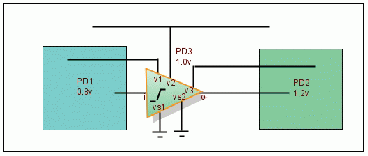
Figure5-1 shows a power domain at 0.8V and one at 1.2V. The ground voltage for both domains is 0.0V. In this case, for data signals going from the domain at 0.8V to the domain at 1.2V a power level shifter with direction up is needed, while for data signals going from the domain at 1.2V to the domain at 0.8V a power level shifter with direction down is needed.
Figure 5-1 Power Level Shifter
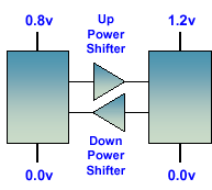
Sample commands to model these power level shifters are:
define_level_shifter_cell  -cells up_shift \
   	 -input_voltage_range 0.8:1.0 -output_voltage_range 1.0:1.2 \
   	 -input_power_pin VDD_IN -output_power_pin VDD_OUT -ground VSS_IN \
   	 -direction up  -valid_location from
define_level_shifter_cell  -cells down_shift \
   	 -input_voltage_range 1.0:1.2 -output_voltage_range 0.8:1.0 \
   	 -input_power_pin VDD_IN -output_power_pin VDD_OUT -ground VSS_IN \
   	 -direction down -valid_location from
Modeling a Ground Level Shifter
To model ground level shifter use the define_level_shifter_cell command with the following options.
- define_level_shifter_cell
-
-cells
cell_list[-library_setlibrary_set]- [-always_on_pins
pin_list]-ground_input_voltage_rangevoltage_list|voltage_range_list}-ground_output_voltage_rangevoltage_list|voltage_range_list}- [-direction {up|down|bidir}]
- [-
input_ground_pinLEF_power_pin]output_ground_pinLEF_power_pin]- [-
powerLEF_ground_pin] - [-always_on_pins
The two power domains in Figure5-2 have the same power supply 1.2V. However, the ground voltage for the first domain is at 0.0V, while the ground voltage for the second domain is at 0.5V. For data signals going from the domain with ground voltage 0.0V to the domain with ground voltage 0.5V a ground level shifter with direction up is required. For data signals going from the domain with ground voltage 0.5V to the domain with ground voltage 0.0V a ground level shifter with direction down is required.
Figure 5-2 Ground Level Shifter
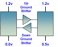
Sample commands to model these ground level shifters are:
define_level_shifter_cell  -cells up_shift \
   	 -ground_input_voltage_range 0.0:0.1 -ground_output_voltage_range 0.4:0.5 \
   	 -input_ground_pin VSS_IN -output_ground_pin VSS_OUT -power VDD_IN \
   	 -direction up  -valid_location from
define_level_shifter_cell  -cells down_shift \
   	 -ground_input_voltage_range 0.4:0.5 -ground_output_voltage_range 0.0:0.1 \
   	 -input_ground_pin VSS_IN -output_ground_pin VDD_OUT -power VDD_IN \
   	 -direction down -valid_location from
Modeling a Power and Ground Level Shifter
To model a power and ground level shifter, use two define_level_shifter_cell commands: one which defines the power level shifting and one which defines the ground level shifting. Both commands must point to the same cell(s), and must have the same value for the -valid_location option.
- define_level_shifter_cell
-
-cells
cell_list[-library_setlibrary_set]- [-always_on_pins
pin_list]-input_voltage_rangevoltage_list|voltage_range_list}-output_voltage_rangevoltage_list|voltage_range_list}- [-direction {up|down|bidir}]
- [-
input_power_pinLEF_power_pin]output_power_pinLEF_power_pin]- [-
groundLEF_ground_pin] - [-always_on_pins
- define_level_shifter_cell
-
-cells
cell_list[-library_setlibrary_set]- [-always_on_pins
pin_list]-ground_input_voltage_rangevoltage_list|voltage_range_list}-ground_output_voltage_rangevoltage_list|voltage_range_list}- [-direction {up|down|bidir}]
- [-
input_ground_pinLEF_power_pin]output_ground_pinLEF_power_pin]- [-
powerLEF_ground_pin] - [-always_on_pins
The two power domains in Figure 5-3 have different power and ground voltages. Going from domain_1 to the domain_2 requires an power level shifter in the up direction and a ground level shifter in the down direction. Going from domain_2 to domain_1 requires a power level shifter in the down direction and a ground level shifter in the up direction.
Figure 5-3 Power and Ground Level Shifter
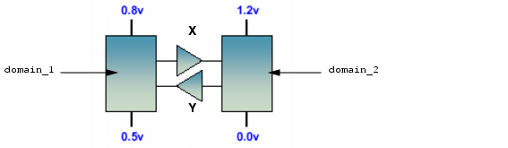
The following commands models the power and ground level shifter to go from domain_1 to domain_2:
define_level_shifter_cell -cells X \-input_voltage_range 0.8:1.0 -output_voltage_range 1.0:1.2 \
-input_power_pin VDD_IN -output_power_pin VDD_OUT -ground VSS_IN \
-direction up -valid_location from
define_level_shifter_cell -cells X-ground_input_voltage_range 0.4:0.5 -ground_output_voltage_range 0.0:0.1 \
-input_ground_pin VSS_IN -output_ground_pin VSS_OUT -power VDD_OUT \
-direction down -valid_location from
Both commands refer to the same cell, use the same valid location and have opposite directions for the power and ground level shifting.
The following commands models the power and ground level shift to go from domain_2 to domain_1:
define_level_shifter_cell -cells Y \-input_voltage_range 1.0:1.2 -output_voltage_range 0.8:1.0 \
-input_power_pin VDD_OUT -output_power_pin VDD_IN -ground VSS_OUT \
-direction down -valid_location to
define_level_shifter_cell -cells Y \-ground_input_voltage_range 0.0:0.1 -ground_output_voltage_range 0.4:0.5 \
-input_ground_pin VSS_OUT -output_ground_pin VSS_OUT -power VDD_OUT \
-direction up -valid_location to
Modeling an Enabled Level Shifter
To model a level shifter that can also be used for isolation purposes, use the define_level_shifter_cell command with the -enable option.
This type of cell uses an enable pin to control the voltage shifting. Typically the enable pin is related to the output supplies of the level shifter. In other words, the enable control needs to have the same voltage as the to domain. If both domains are powered on, you can tie the enable to be always active and it works as a level shifter.
 | To model an isolation-level-shifter combo cell, see Modeling an Isolation-Level Shifter Combo Cell. |
Modeling an Enabled Power Level Shifter
Assume that the power level shifter shown in Figure 5-1 also has an enable pin to enable the level-shifting functionality. If the enable signal is inactive for the level shifting purposes, it protects the level shifter cell when the input power supply is powered down and causes the output to be a specific logic value determined by its functionality. However, the driver of the level shifter data pin is not protected. For such a cell to be used for isolation purposes when the driving domain is switched off using a header power switch, its input power pin must be connected to the primary power net of the driving domain. In this case the definition should be adjusted as follows:
define_level_shifter_cell -cells up_shift \
-input_voltage_range 0.8:1.0 -output_voltage_range 1.0:1.2 \
-input_power_pin VDD_IN -output_power_pin VDD_OUT -ground VSS_IN \
-direction up -valid_location from \-enable en
Where en is the enable pin that controls the power shifting. Typically the enable pin is related to the output supplies of the level shifter.
Modeling an Enabled Ground Level Shifter
Assume that the ground level shifter shown in Figure 5-2 also has an enable pin to enable the level-shifting functionality. If the enable signal is inactive for the level shifting purposes, it protects the level shifter cell when the input ground supply is shut off and causes the output to be a specific logic value determined by its functionality. However, the driver of the level shifter data pin is not protected. For such a cell to be used for isolation purposes when the driving domain is switched off using a footer ground switch, its input ground pin must be connected to the primary ground net of the driving domain. In this case the definition should be adjusted as follows:
define_level_shifter_cell -cells down_shift \
-ground_input_voltage_range 0.4:0.5 -ground_output_voltage_range 0.0:0.1 \
-input_ground_pin VSS_IN -output_ground_pin VDD_OUT -power VDD_IN \
-direction down -valid_location from \-enable en
Where en is the enable pin that controls the ground shifting. Typically the enable pin is related to the output supplies of the level shifter.
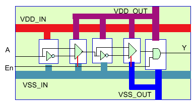
Modeling an Enabled Power and Ground Level Shifter
For power and ground level shifter cells, the enable pin needs to be specified with the definition of the power (ground) level shifter depending on whether the pin needs to control the power (ground) shifting. The layout of the cell determines whether it can be used in a domain that is power-switched (using a header switch cell) or ground-switched (using a footer switch cell). This section will illustrate a couple of examples.
In all examples, data signal A is driven by a power domain whose power and ground supply connects to VDD_IN and VSS_IN, respectively. The data output signal Y feeds in to a domain whose power and ground supply connects to VDD_OUT and VSS_OUT, respectively. This requires a power and ground level shifter cell. In the following examples, the following relations apply:
VSS_OUT < VSS_IN
VDD_OUT > VDD_IN
In addition, because the power domain driving A can be switched off, the level shifter must also be an enabled shifter. The required type of the enabled power and ground shifter will depend on whether the power domain is power or ground switched and on where the enabling logic gets is power and ground supply from.
Example 1
The type of level shifter shown in Figure 5-4, can be used when the power domain driving signal A is ground switched. The power and ground of the enabling logic are connected to VDD_OUT and VSS_OUT, respectively.
Figure 5-4 Type 1: Ground Shifter in Input Stage and Enabling Logic in Output Stage
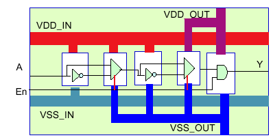
The following CPF commands describe this type 1 power and ground enabled level shifter:
define_level_shifter_cell -cells X \
-ground_input_voltage_range 0.2:0.3 -ground_output_voltage_range 0.1:0.2 \
-input_ground_pin VSS_IN -output_ground_pin VSS_OUT -powerVDD_IN\
-direction down -valid_location from
define_level_shifter_cell -cells X \
-input_voltage_range 0.8:1.0 -output_voltage_range 1.0:1.2 \
-input_power_pin VDD_IN -output_power_pin VDD_OUT -groundVSS_OUT\
-direction up -valid_location from-enable en
Example 2
The type of level shifter shown in Figure 5-5, can be used when the power domain of signal A is power switched. The power and ground of the enabling logic are connected to VDD_OUT and VSS_OUT, respectively.
Figure 5-5 Type 2: Power Shifter in Input Stage and Enable Logic in Output Stage
The following CPF commands describe this type 2 of power and ground enabled level shifter:
define_level_shifter_cell -cells X \
-ground_input_voltage_range 0.2:0.3 -ground_output_voltage_range 0.1:0.2 \
-input_ground_pin VSS_IN -output_ground_pin VSS_OUT -powerVDD_OUT\
-direction down -valid_location from-enable en
define_level_shifter_cell -cells X \
-input_voltage_range 0.8:1.0 -output_voltage_range 1.0:1.2 \
-input_power_pin VDD_IN -output_power_pin VDD_OUT -groundVSS_IN\
-direction up -valid_location from
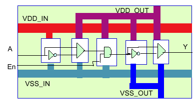
Example 3
The type of level shifter shown in Figure 5-6, can be used when the power domain is ground switched. The power and ground of the enabling logic are connected to VDD_IN and VSS_OUT, respectively.
Figure 5-6 Type 3: Ground Shifter and Enable Logic in Input Stage
The following CPF commands describe this type 3 of power and ground enabled level shifter:
define_level_shifter_cell -cells X \
-ground_input_voltage_range 0.2:0.3 -ground_output_voltage_range 0.1:0.2 \
-input_ground_pin VSS_IN -output_ground_pin VSS_OUT -powerVDD_IN\
-direction down -valid_location from-enable en
define_level_shifter_cell -cells X \
-input_voltage_range 0.8:1.0 -output_voltage_range 1.0:1.2 \
-input_power_pin VDD_IN -output_power_pin VDD_OUT -groundVSS_OUT\
-direction up -valid_location from
Example 4
The type of level shifter shown in Figure 5-7, can be used when the power domain is power switched. The power and ground of the enabling logic are connected to VDD_OUT and VSS_IN, respectively.
Figure 5-7 Type 4: Power Shifter and Enable Logic in Input Stage
The following CPF commands describe this type 4 of power and ground enabled level shifter:
define_level_shifter_cell -cells X \
-ground_input_voltage_range 0.2:0.3 -ground_output_voltage_range 0.1:0.2 \
-input_ground_pin VSS_IN -output_ground_pin VSS_OUT -powerVDD_OUT\
-direction down -valid_location from
define_level_shifter_cell -cells X \
-input_voltage_range 0.8:1.0 -output_voltage_range 1.0:1.2 \
-input_power_pin VDD_IN -output_power_pin VDD_OUT -groundVSS_IN\
-direction up -valid_location from-enable en
Modeling a Bypass Level Shifter
To model a level shifter whose level shifting functionality can be bypassed under certain conditions, use the define_level_shifter_cell command with the -bypass_enable option.
An example of such a cell is shown in Figure5-8. When the bp_enable signal is true, the level shifting functionality is bypassed and signal OUT will be coming from the top buffer.
Figure 5-8 Bypass Level Shifter Cell
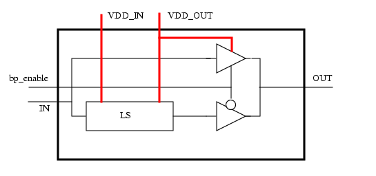
The following CPF command can be used to describe a bypass level shifter:
define_level_shifter_cell -cells up_shift \
-input_voltage_range 0.8:1.0 -output_voltage_range 1.0:1.2 \
-input_power_pin VDD_IN -output_power_pin VDD_OUT -ground VSS \
-direction up -valid_location from-bypass_enable bp_enable
To apply such a cell for a specific level shifter rule, you need to use the -bypass_condition option of the create_level_shifter_rule command to indicate the signal for the bypass enable pin for the cell.
Modeling a Multi-Stage Level Shifter
When the voltage difference between the driving (or originating) and receiving (or destination) power domains is large, multiple level shifters or a single multi-stage level shifter might be required.
To model a single multi-stage level shifter cell, define the level-shifter cell with the -multi_stage option in the define_level_shifter_cell command to identify the stage of the multi-stage level shifter to which this definition (command) applies.
For a level shifter cell with N stages, N definitions must be specified for the same cell. Each definition must associate a number from 1 to N for this option to indicate the corresponding stage of this definition. A definition must not have the same stage defined twice.
An example of a single multi-stage level-shifter cell is shown in Figure 5-9.
Figure 5-9 Multi-Stage Level Shifter
The following CPF commands can be used to describe the single level shifter cell shown in Figure 5-9.
define_level_shifter_cell -cells fooA-multi_stage 1-input_power_pin V1 \
-output_power_pin V2 -input_ground_pin VS1 -output_ground_pin VS2
define_level_shifter_cell -cells fooA-multi_stage 2-input_power_pin V2 \
-input_ground_pin VS2 -output_voltage_pin V3 -output_ground_pin VS2
When you define the level shifter rule, you can indicate in the update_level_shifter_rules command whether to use a single multi-stage level-shifter cell or an ordered list of level-shifter cells:
To use a single multi-stage level-shifter cell you must use the
-throughoption to specify the subsequent domains for the multi-stage level shifting between the first domain (specified with-fromin thecreate_level_shifter_rulecommand) and the last domain (specified with-toin thecreate_level_shifter_rulecommand).In this case, the cell must have been defined with the
-multi_stageoption in thedefine_level_shifter_cellcommand.To use multiple cells, you must specify an ordered list of N cell lists for the
-cellsoption, where N is the number of stages in the level-shifting. Each list contains the cells appropriate for its stage.
Modeling a Multi-bit Level Shifter Cell
A multi-bit level shifter cell has multiple pairs of input and output pins with each pair serving as a single bit level shifter. An example is shown in Figure 5-10.
For the following multi-bit level shifter cells, there is no difference in modeling such a multi-bit cell with respect to the single bit level shifter cell:
a multi-bit simple level shifter without an enable pin
a multi-bit enable level shifter with the same enable pin for all bits
If the cell has different enable pins for the input and output pairs, you must model the cell using the -pin_groups option of the define_level_shifter_cell command.
Figure 5-10 Multi-Bit Level Shifter
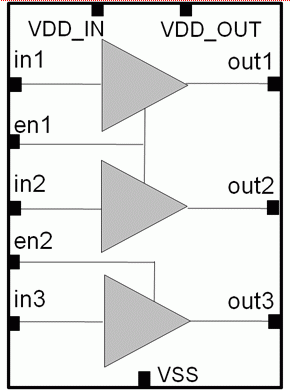
The following CPF command can be used to describe the multi-bit level shifter cell shown in Figure 5-10.
define_level_shifter_cell -cells multi_bit_en \
-input_voltage_range 0.8:1.0 -output_voltage_range 1.0:1.2 \
-input_power_pin VDD_IN -output_power_pin VDD_OUT -ground VSS \
-direction up -valid_location from \-pin_groups {{in1 out1 en1} {in2 out2 en1} {in3 out3 en2}}
Note:
-pin_groups is a new option introduced in the SI2 CPF 2.0 version.
Modeling Isolation Cells
Modeling an Isolation Cell to be Placed in the Unswitched Domain
Modeling An Isolation Cell for Ground Switchable Domain
Modeling An Isolation Cell for Power Switchable Domain
Modeling An Isolation Cell for Power and Ground Switchable Domains
Modeling An Isolation Cells that Can Be Placed in Any Domain
Modeling An Isolation Cells that Can Be Placed in Any Domain
Modeling An Isolation Clamp Cell
Modeling an Isolation-Level Shifter Combo Cell
Modeling an Isolation Cell with Multiple Enable Pins
Modeling an Isolation Latch with a Set or Reset Pin
Modeling a Multi-bit Isolation Cell
Types of Isolation Cells
Isolation logic is required when the leaf drivers and leaf loads of a net are in power domains that are not on and off at the same time, or because it is part of the design intent. CPF can describe many different types of isolation cells. Below is a list of the most typical isolation cells:
Isolation cell to be placed in the unswitched domain
Isolation cell to be used in a ground switchable domain
Isolation cell to be used in a power switchable domain
Isolation cells to be used in a a power or ground switchable domain
Isolation cells without followpins that can be placed in any domain
Isolation cells without an enable pin
Isolation clamp cell
Isolation-level shifter combo cell
All types of isolation cells are defined using the define_isolation_cell command. The following sections indicate which command options to use for each type.
Modeling an Isolation Cell to be Placed in the Unswitched Domain
To model an isolation cell to be placed in an unswitched domain, use the define_isolation_cell command with the following options.
- define_isolation_cell
-
-cells
cell_list[-library_setlibrary_set]- -power
LEF_power_pin-groundLEF_ground_pin-valid_location on{ -enablepin| -no_enable {high|low|hold} } [-non_dedicated] - -power
Figure 5-11 shows an AND cell that can be used for isolation purposes.
Figure 5-11 Dedicated Isolation Cell in Unswitched Domain
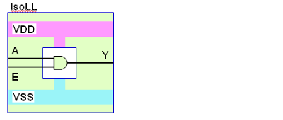
The following command models the isolation cell in Figure 5-11:
define_isolation_cell \
   	 -cells IsoLL \
   	 -power VDD -ground VSS \
   	 -enable E \
   	 -valid_location on
Note:
If you also want to use the cell in regular logic, you must add the -non_dedicated option. Non-dedicated cells can typically only be placed in the unswitched domain (-valid_location on).
Modeling An Isolation Cell for Ground Switchable Domain
To model an isolation cell to be used in a ground switchable domain, use the define_isolation_cell command with the following options.
- define_isolation_cell
-
-cells
cell_list[-library_setlibrary_set]- [-always_on_pins
pin_list]-ground_switchableLEF_ground_pin-powerLEF_power_pin-groundLEF_ground_pin[-valid_location { from | to | on | off}]- { -enable
pin| -no_enable {high|low|hold} } [-non_dedicated] - [-always_on_pins
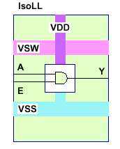
Figure 5-12 shows an AND cell that has the path from power to ground cut off on the ground side. This AND cell can only be used for isolation.
Figure 5-12 Dedicated Ground Switchable Isolation Cell
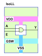
The following command models the isolation cell in Figure 5-12:
define_isolation_cell \
-cells IsoLL \
-ground_switchableGSW \
-power VDD -ground VSS \
-enable E \
-valid_location from
Modeling An Isolation Cell for Power Switchable Domain
To model an isolation cell to be used in a power switchable domain, use the define_isolation_cell command with the following options.
- define_isolation_cell
-
-cells
cell_list[-library_setlibrary_set]- [-always_on_pins
pin_list]-power_switchableLEF_power_pin- -power
LEF_power_pin-groundLEF_ground_pin[-valid_location { from | to | on | off}]- { -enable
pin| -no_enable {high|low|hold} } - [-always_on_pins
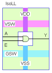
Figure 5-13 shows an AND cell that has the path from power to ground cut off on the power side. This AND cell can only be used for isolation.
Figure 5-13 Dedicated Power Switchable Isolation Cell
The following command models the isolation cell in Figure 5-13:
define_isolation_cell \
-cells IsoLL \
-power_switchableVSW \
-power VDD -ground VSS \
-enable E \
-valid_location from
Modeling An Isolation Cell for Power and Ground Switchable Domains
To model an isolation cell to be used in a power and ground switchable domain, use the define_isolation_cell command with the following options.
- define_isolation_cell
-
-cells
cell_list[-library_setlibrary_set]- [-always_on_pins
pin_list]-power_switchableLEF_power_pin-ground_switchableLEF_ground_pin-powerLEF_power_pin-groundLEF_ground_pin[-valid_location { from | to | on | off}]- { -enable
pin| -no_enable {high|low|hold} } - [-always_on_pins
Figure 5-14 shows an AND cell that has the path from power to ground cut off on the power and ground sides. This AND cell can only be used for isolation.
Figure 5-14 Dedicated Power and Ground Switchable Isolation Cell
The following command models the isolation cell in Figure 5-14:
define_isolation_cell \
-cells IsoLL \
-power_switchableVSW-ground_switchableGSW \
-power VDD -ground VSS \
-enable E \
-valid_location from
Modeling An Isolation Cells that Can Be Placed in Any Domain
To model an isolation cell to be used in any domain, use the define_isolation_cell command with the following options.
- define_isolation_cell
-
-cells
cell_list[-library_setlibrary_set]- [-always_on_pins
pin_list]- -power
LEF_power_pin-groundLEF_ground_pin-valid_location any{ -enablepin| -no_enable {high|low|hold} }- [-non_dedicated]
- [-always_on_pins
Modeling An Isolation Cell Without Enable Pin
There are special isolation cells which do not have an enable pin but still can clamp output to a logic value when primary power supply is switched off. To model such a cell, use define_isolation_cell command with the following options.
- define_isolation_cell
-
-cells
cell_list[-library_setlibrary_set]- [-always_on_pins
pin_list]- [-power_switchable
LEF_power_pin] [-ground_switchableLEF_ground_pin]- [-power
LEF_power_pin] [-groundLEF_ground_pin]- [-valid_location { from | to | on | off | any}]
-no_enable {high|low|hold} - [-always_on_pins
Note:
You can only infer such cells in a design by specifying the create_isolation_rule command with -no_condition option.
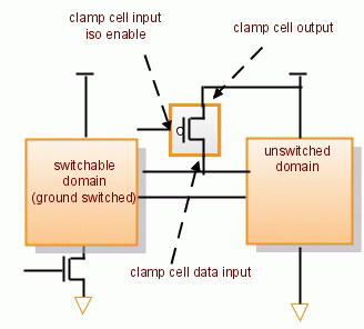
Modeling An Isolation Clamp Cell
An isolation clamp high cell is a simple PMOS transistor with the gate input being used as the enable pin. When its driver is switched off by a ground switch and the enable pin has value 0, the connected net can be clamped to a logic high value as shown in Figure 5-15.
Figure 5-15 Isolation clamp high cell
To model an isolation clamp high cell, use the define_isolation_cell command with the following options.
- define_isolation_cell
-
-cells
cell_list[-library_setlibrary_set]- [-always_on_pins
pin_list]-powerLEF_power_pin[-valid_location { from | to | on | off | any}]- -enable
pin-clamp high[-non_dedicated] - [-always_on_pins
An isolation clamp low cell is a simple NMOS transistor with the gate input being used as the enable pin. When its driver is switched off by a power switch and the enable pin has value 1, the connected net can be clamped to a logic low value as shown in Figure 5-16.
Figure 5-16 Isolation clamp low cell
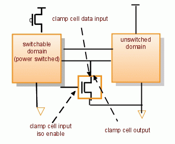
To model an isolation clamp low cell, use the define_isolation_cell command with the following options.
- define_isolation_cell
-
-cells
cell_list[-library_setlibrary_set]- [-always_on_pins
pin_list]-groundLEF_ground_pin[-valid_location { from | to | on | off | any}]- -enable
pin-clamp low- [-non_dedicated]
- [-always_on_pins
Due to its special connectivity requirement, to apply such a power or ground clamp cell for a specific isolation rule, you need to use -isolation_output option with either the clamp_high or clamp_low value in the create_isolation_rule command.
Modeling an Isolation-Level Shifter Combo Cell
A combo cell isolates or protects the input when the driving logic is powered down and generates an output isolation value at the same voltage as the output supply of the cell. Typically the enable pin is related to the input supplies of the cell.
The most common combo cells are the isolation cells with high to low shifting capabilities.
To model a combo cell you need two commands. For example to model an isolation cell for power switchable domain that is also a power level shifter, use the following definitions:
- define_isolation_cell
-
-cells
cell_list[-library_setlibrary_set]- [-always_on_pins
pin_list]-power_switchableLEF_power_pin- -power
LEF_power_pin-groundLEF_ground_pin[-valid_location {to | from}]- { -enable
pin| -no_enable {high|low|hold} } [-non_dedicated] - [-always_on_pins
- define_level_shifter_cell
-
-cells
cell_list[-library_setlibrary_set]- [-always_on_pins
pin_list]-input_voltage_rangevoltage|voltage_range}-output_voltage_rangevoltage|voltage_range}- -direction down
- [-
input_power_pinLEF_power_pin]output_power_pinLEF_power_pin]- [-
groundLEF_ground_pin] - [-always_on_pins
Note:
You cannot use the -enable option in the define_level_shifter_cell definition.In addition, you must specify the same value for the -valid_location option in both commands.
| If you want to model an enabled level shifter, see Modeling an Enabled Level Shifter. |
Modeling an Isolation Cell with Multiple Enable Pins
Some isolation cells have besides an enable pin that is related to the non-switchable supply of the cell, additional enable pins that are related to the switchable supply. The switchable enable pin can be used to synchronize the isolation logic right before the non-switchable enable pin is activated or deactivated. To model an isolation cell with multiple enable pins, use the define_isolation_cell command with the following options.
- define_isolation_cell
-
-cells
cell_list[-library_setlibrary_set]-aux_enablespin_list[-power_switchableLEF_power_pin] [-ground_switchableLEF_ground_pin]- [-power
LEF_power_pin] [-groundLEF_ground_pin]- [-valid_location {from | to | on | off | any}]
-enablepin[-clamp {high|low}]
When you specify an isolation rule that targets these types of isolation cells, you need to use the create_isolation_rule command with the -isolation_control option with control type sync_enable.
Figure 5-17shows two examples of cells with multiple enable pins. The iso enable pin is related to the non-switchable supply vddc, while the en enable pin is related to the switchable supply vdd.
Figure 5-17 Isolation Cells with Multiple Enable Pins
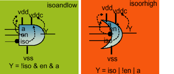
The following command models the isoandlow and isoorhigh cells in Figure 5-17:
- define_isolation_cell \
-
-cells {isoandlow isoorhigh} \
-aux_enablesen \- -power_switchable vdd \
- -power vddc -ground vss \
- -enable iso
The following commands show the isolation rules that target the isoandlow and isoorhigh cells in Figure 5-17:
- create_isolation_rule \
-
-name iso1 \
- -isolation_condition iso_drvr \
- -from PD1 \
- -isolation_output low \
-isolation_control{ {sync_enable en_drvr} } \- -secondary_domain iso_supply_domain
- -isolation_condition iso_drvr \
- create_isolation_rule \
-
-name iso2 \
- -isolation_condition iso_drvr \
- -from PD1 \
- -isolation_output high \
-isolation_control{ {sync_enable en_drvr} } \- -secondary_domain iso_supply_domain
- -isolation_condition iso_drvr \
Modeling an Isolation Latch with a Set or Reset Pin
Some isolation latches are designed with a set or reset pin to ensure that the latch output has a known value at the time when the design is initially powered up. To model an isolation latch with a set or reset pin, use the define_isolation_cell command with the following options.
- define_isolation_cell
-
-cells
cell_list[-library_setlibrary_set]-always_on_pinspin_list[-power_switchableLEF_power_pin] [-ground_switchableLEF_ground_pin]- [-power
LEF_power_pin] [-groundLEF_ground_pin]- [-valid_location {from | to | on | off | any}]
-enablepin[-clamp {high|low}]
When you specify an isolation rule that targets these types of isolation cells, you need to use the create_isolation_rule command with the -isolation_control option with control type set or reset and the -isolation_output option with value hold.
Figure 5-18 shows two examples of such latches. The iso enable pin, isoprez (set), the isoclr (reset) pins are all related to the non-switchable supply vddc.
Figure 5-18 Isolation Cells with Set and Reset Pins
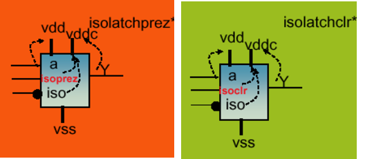
The following commands model the isolatchclr and isolatchprez cells in Figure 5-18:
- define_isolation_cell
-
-cells isolatchclr
-always_on_pinsisoprez- -power_switchable vdd
- -power vddc -ground vss
- -enable iso
- define_isolation_cell
-
-cells isolatchclr
-always_on_pinsisoclr- -power_switchable vdd
- -power vddc -ground vss
- -enable iso
The following commands show the isolation rules that targets the isolatchclr and isolatchprez cells in Figure 5-18:
- create_isolation_rule \
-
-name iso1 \
- -isolation_condition iso_drvr \
- -from PD1
- -isolation_output hold \
-isolation_control{ {set iso_prez} } \- -secondary_domain iso_supply_domain
- -isolation_condition iso_drvr \
- create_isolation_rule \
-
-name iso2 \
- -isolation_condition iso_drvr \
- -from PD1 \
- -isolation_output hold \
-isolation_control{ {reset iso_clr} } \- -secondary_domain iso_supply_domain
- -isolation_condition iso_drvr \
Modeling a Multi-bit Isolation Cell
A multi-bit isolation cell has multiple pairs of input and output pins with each pair serving as a single bit isolation cell. An example is shown in Figure 5-19.
If the cell uses the same enable pin for all pairs of input and output pins, there is no difference in modeling such a multi-bit cell with respect to the single bit isolation cell.
If the cell has different enable pins for the input and output pairs, you must model the cell using the -pin_groups option of the define_isolation_cell command.
Figure 5-19 Multi-bit Isolation Cell
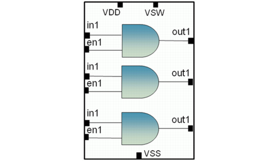
The following CPF command can be used to describe the multi-bit isolation cell for power switchable domain shown in Figure 5-19 (see Figure 5-13 for the corresponding single bit cell).
define_isolation_cell -cells IsoLL \
-power_switchable VSW \
-power VDD -ground VSS \-pin_groups {{in1 out1 en1} {in2 out2 en2} {in3 out3 en3}}
Modeling a Complex Isolation Cell
For complex isolation cells that cannot be modeled using the previous techniques, CPF provides a generic mechanism.
To model a complex isolation cell, use the update_isolation_rules command with the following options.
update_isolation_rules-namesrule_list-cellscell_list[-use_model-pin_mappingpin_mapping_list[-domain_mappingdomain_mapping_list] ]
In this case, the first cell specified in the cell list refers to the complicated isolation cell that cannot be modelled using the define_isolation_cell command. The cell name that you specify must correspond to both the model name used in simulation and the cell name used for implementation.
Use the following format for the pin_mapping_list to specify the connection of each cell pin to a pin or port in the design:
{cell_pindesign_pin_reference}
cell_pinis the name of the pin in the cell definitiondesign_pin_referenceis one of the following:
If the cell has a corresponding macro model definition in CPF, you can specify the mapping of the domains in the macro model to the top-level domains.
Use the following format to specify a domain mapping:
{domain_in_child_scopedomain_in_parent_level_scope}
The specified domain mapping applies to all instantiations of the specified isolation cell.
If the macro model has multiple power domains defined, this option must be used.
Modeling State Retention Cells
Types of State Retention Cells
State Retention Cell that Restores when Power is Turned On
State Retention Cell that Restores when Control Signal is Deactivated
State Retention Cells with Save and Restore Controls
State Retention Cells without Save or Restore Control
Types of State Retention Cells
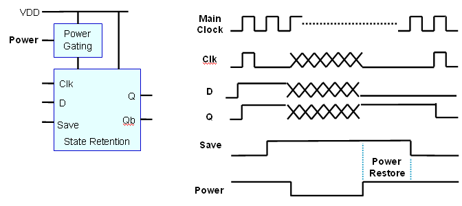
State retention cells are used for sequential cells to keep their previous state prior to power down.
CPF can describe different types of state retention cells. The following is a list of the most typical state retention cells:
State Retention Cell with Save Control
State Retention Cell with Restore Control
State Retention Cells with Save and Restore Controls
State Retention Cells without Save or Restore Control
All types of state retention cells are defined using the define_state_retention_cell command. The following sections indicate which command options to use for each type.
State Retention Cell that Restores when Power is Turned On
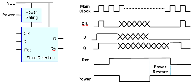
To model a state retention cell that saves the current value when the control pin becomes active while the power is on, retains the saved value when power is off, and restores the saved value when the power is turned on, use the following command options:
define_state_retention_cell
-cellscell_list[-library_setlibrary_set]
[-cell_typestring]
[-always_on_pinspin_list][-clock_pinpin]
-save_functionexpression[-restore_checkexpression] [-save_checkexpression]
[-always_on_componentscomponent_list]
[ {-power_switchableLEF_power_pin
|-ground_switchableLEF_ground_pin|-power_switchableLEF_power_pin-ground_switchableLEF_ground_pin}
-powerLEF_power_pin-groundLEF_ground_pin]
Figure 5-20 shows an example of such a cell.
Figure 5-20 State Retention with Save Control
To model the cell shown in Figure 5-20, use the following command:
define_state_retention_cell -cells SR1 \
-clock_pin Clk \
-save_functionsave \
-restore_check!Clk-save_check!Clk \
-power_switchable VSW \
-power VDD -ground VSS
State Retention Cell that Restores when Control Signal is Deactivated
To model a state retention cell that saves the current value when the control pin becomes deactivated and restores the saved value when the control signal becomes activated, use the following command options:
define_state_retention_cell
-cellscell_list[-library_setlibrary_set]
[-cell_typestring]
[-always_on_pinspin_list][-clock_pinpin]
-restore_functionexpression[-restore_checkexpression] [-save_checkexpression]
[-always_on_componentscomponent_list]
[ {-power_switchableLEF_power_pin
|-ground_switchableLEF_ground_pin|-power_switchableLEF_power_pin-ground_switchableLEF_ground_pin}
-powerLEF_power_pin-groundLEF_ground_pin]
Figure 5-21 shows an example of such a cell.
Figure 5-21 State Retention with Restore Control
To model the cell shown in Figure 5-21, use the following command:
define_state_retention_cell -cells SR1 \
-clock_pin Clk \
-restore_function!Ret \
-restore_check!Clk-save_check!Clk \
-power_switchable VSW \
-power VDD -ground VSS
State Retention Cells with Save and Restore Controls
If you have a state retention cell with both save and restore control, the cell saves the current value when the save control pin is activated and the power is on, while the cell restores the saved value when the restore control pins is activated. To model such a cell use the following command options:
define_state_retention_cell
-cellscell_list[-library_setlibrary_set]
[-cell_typestring]
[-always_on_pinspin_list][-clock_pinpin]
-restore_functionexpression-save_functionexpression[-restore_checkexpression] [-save_checkexpression]
[-always_on_componentscomponent_list]
[ {-power_switchableLEF_power_pin
|-ground_switchableLEF_ground_pin|-power_switchableLEF_power_pin-ground_switchableLEF_ground_pin}
-powerLEF_power_pin-groundLEF_ground_pin]
In this case, the cell saves the current value when the save expression is true and the power is on. The cell restores the saved value when the restore expression is true and the power is on.
It is an error if you use the same pin or same expressions for both the save and restore function. For example the following two commands are not correct:
define_state_retention_cell -cells My_Cell -restore_function pg -save_function !pg
define_state_retention_cell -cells foo -restore_function pg -save_function pg
Figure 5-22 shows an example of such a cell.
Figure 5-22 State Retention with Save and Restore Controls
To model the cell shown in Figure 5-22, use the following command:
define_state_retention_cell -cells SR2 \
-clock_pin Clk \
-restore_functionWake-save_functionSleep \
-restore_check"!Clk"-save_check"!Clk" \
-power_switchable VSW \
-power VDD -ground VSS
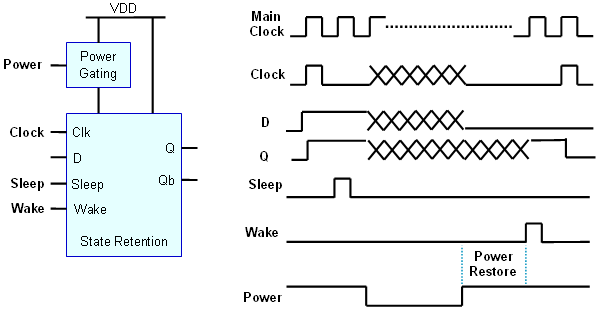
The state will be saved when Sleep is active and the clock is down and the state will also be restored when Wake is active and the clock is down.
State Retention Cells without Save or Restore Control
A master-slave type state retention cell does not have a save or restore control pin. It has a secondary power or ground pin to provide continuous power supply to the slave latch. The clock signal acts as the retention control signal. As a result, you should use the clock signal for the registers as the restore edge and save edge.
When the clock signal is used as the restore or save signal for a flop, then the synthesis tool will synthesize it using a master-slave type retention cell. For library definition, the clock pin needs to be declared as the only save and restore signal and has to be an always-on pin.
To model such a cell use the following command options:
define_state_retention_cell
-cellscell_list[-library_setlibrary_set]
[-cell_typestring]
[-always_on_pinspin_list][-clock_pinpin]
-save_functionexpression[-restore_checkexpression] [-save_checkexpression]
[-always_on_componentscomponent_list]
[ {-power_switchableLEF_power_pin
|-ground_switchableLEF_ground_pin|-power_switchableLEF_power_pin-ground_switchableLEF_ground_pin}
-powerLEF_power_pin-groundLEF_ground_pin]
When you specify a state retention rule that targets these types of state retention cells, you need to use the create_state_retention_rule command with the -save_edge option and the clock signal in the expression.
The following example models master-slave retention cell ms_ret:
define_state_retention_cell -cells ms_ret \
-clock_pin CLK \
-save_functionCLK \
-restore_check "!CLK" -save_check "!CLK"
The following command shows the state retention rule that targets cell ms_ret
create_state_retention_rule -name sr1 \
-domain PD1 \
-save_edgeclock
Modeling a Complex State Retention Cell
For complex state retention cells that cannot be modeled using the previous techniques, CPF provides a generic mechanism. To model such a cell, use the update_isolation_rules command with the following options.
update_state_retention_rules-namesrule_list-cellscell_list[-use_model-pin_mappingpin_mapping_list[-domain_mappingdomain_mapping_list] ]
In this case, the first cell specified in the cell list refers to the complicated state retention cell that cannot be modelled using the define_state_retention_cell command. The cell name that you specify must correspond to both the model name used in simulation and the cell name used for implementation.
Use the following format for the pin_mapping_list to specify the connection of each cell pin to a pin or port in the design:
{cell_pindesign_pin_reference}
cell_pinis the name of the pin in the cell definitiondesign_pin_referenceis one of the following:the name of a design port or instance pin. You can prepend the "!" character to the name if the inverse of the port/pin is used to drive the cell pin
save_signal, which refers to the expression in-save_edgeor-save_leveloptionrestore_signal, which refers to the expression in-restore_edgeor-restore_leveloption
If the cell has a corresponding macro model definition in CPF, you can specify the mapping of the domains in the macro model to the top-level domains.
Use the following format to specify a domain mapping:
{domain_in_child_scopedomain_in_parent_level_scope}
The specified domain mapping applies to all instantiations of the specified state retention cell.
If the macro model has multiple power domains defined, this option must be used.
Modeling Power Switch Cells
Modeling a Single Stage Power Switch Cell
Modeling a Power Switch cell with Gate Bias
Modeling a Single Stage Ground Switch Cell
Modeling a Dual-Stage Power Switch Cell
Types of Power Switch Cells
To connect and disconnect the power (or ground) supply from the gates in internal switchable power domains, you must add power switch logic.
CPF can describe different types of power switch cells. The following is a list of the most typical cells:
single stage power switch cell--single transistor that controls the primary power supply to the logic of an internal switchable domain
single stage ground switch cell--single transistor that controls the primary ground supply to the logic of an internal switchable domain
dual-stage power switch--power switch with a weak and strong transistor to control the primary power supply to the logic of an internal switchable domain
dual-stage ground switch--ground switch with a weak and strong transistor to control the primary ground supply to the logic of an internal switchable domain
All types of power switch cells are defined using the define_power_switch_cell command. The following sections indicate which command options to use for each type.
Modeling a Single Stage Power Switch Cell
To model a single stage power switchable power switch cell use the define_power_switch_cell command with the following options:
- define_power_switch_cell
-
-cells
cell_list[-library_setlibrary_set]-stage_1_enableexpression[-stage_1_outputexpression]- -type
header- -power_switchable
LEF_power_pin-powerLEF_power_pin[-groundLEF_ground_pin]- [-enable_pin_bias [
float:]float] [ -gate_bias_pinLEF_power_pin]- [ -stage_1_on_resistance
float] [ -stage_1_saturation_currentfloat]- [ -leakage_current
float]
In case of an unbuffered power switch cell, you do not need to specify the -stage_1_output and -ground options.
Figure 5-23 shows a power switch cell with an internal buffer. VIN is the pin connected to the unswitched power. VSW is the pin connected to the switchable power that is connected to the logic. When the enable signal Ei is activated the unswitched power is supplied to the logic. As shown in Figure 5-23, this type of cell usually contains a buffer that allows multiple power switch cells to be chained together to form a power switch column or ring. However, the power and ground of this buffer must be unswitchable.
Figure 5-23 Single Stage Power Switch
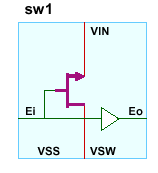
The following command models the power switch cell shown in Figure 5-23:
- define_power_switch_cell \
-
-cells sw1 \
-stage_1_enableEi-stage_1_output- -type
header \VSW- -power_switchable
-powerVIN-groundVSS
Modeling a Power Switch cell with Gate Bias
To model a single stage power switchable power switch cell with gate bias use the define_power_switch_cell command with the following options:
- define_power_switch_cell
-
-cells
cell_list[-library_setlibrary_set]-stage_1_enableexpression[-stage_1_outputexpression]- -type
header- -power_switchable
LEF_power_pin-powerLEF_power_pin[-groundLEF_ground_pin]-enable_pin_bias[float:]float-gate_bias_pinLEF_power_pin[ -stage_1_on_resistancefloat] [ -stage_1_saturation_currentfloat]- [ -leakage_current
float]
Typically the enable pin is related to the power and the ground pin. With gate bias the enable pin is related to the gate bias pin and the ground. The voltage on the gate bias pin is larger than the voltage of the power pin. Such as cell creates less leakage power compared to the cell without gate bias.
In Figure 5-24, the gate bias pin is VGB. Assume that input voltage VIN is at 1.2V and the gate bias pin is at 3.3 V.
Figure 5-24 Single Stage Power Switch with Gate Bias
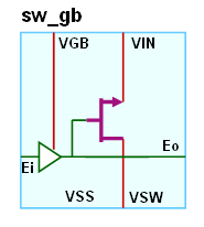
The following command models the power switch cell shown in Figure 5-24:
- define_power_switch_cell \
-
-cells sw1 \
-stage_1_enableEi-stage_1_output- -type
header \VSW- -power_switchable
-powerVIN-groundVSS \- -gate_bias_pin VGB -enable_pin_bias 2.1
Modeling a Single Stage Ground Switch Cell
To model a single stage ground switchable power switch cell use the define_power_switch_cell command with the following options:
- define_power_switch_cell
-
-cells
cell_list[-library_setlibrary_set]-stage_1_enableexpression[-stage_1_outputexpression]- -type
footer- -ground_switchable
LEF_ground_pin-groundLEF_ground_pin[-powerLEF_power_pin]- [-enable_pin_bias [
float:]float] [ -gate_bias_pinLEF_power_pin]- [ -stage_1_on_resistance
float] [ -stage_1_saturation_currentfloat]- [ -leakage_current
float]
Figure 5-25 shows a ground switch cell. VSS is the pin connected to the unswitched ground. VSW is the pin connected to the switchable ground that is connected to the logic. When the enable signal Ei is activated the unswitched ground is supplied to the logic. As shown in Figure 5-25, this type of cell usually contains a buffer that allows multiple ground switch cells to be chained together to form a ground switch column or ring. However the power and ground of this buffer must be unswitchable.
Figure 5-25 Single Stage Ground Switch
The following command models the ground switch cell shown in Figure 5-25:
- define_power_switch_cell \
-
-cells gw1 \
-stage_1_enableEi-stage_1_output- -type
header \GSW- -ground_switchable
-groundVSS-powerVDD
Modeling a Dual-Stage Power Switch Cell
To model a power switch cell with two stages, use the following command options:
- define_power_switch_cell
-
-cells
cell_list[-library_setlibrary_set]-stage_1_enableexpression[-stage_1_outputexpression]-stage_2_enableexpression[-stage_2_outputexpression]- -type
header- -power_switchable
LEF_power_pin-powerLEF_power_pin[-groundLEF_ground_pin]- [-enable_pin_bias [
float:]float] [ -gate_bias_pinLEF_power_pin]- [ -stage_1_on_resistance
float] [ -stage_1_saturation_currentfloat]- [ -stage_2_on_resistance
float] [ -stage_2_saturation_currentfloat]- [ -leakage_current
float]
Figure 5-26 shows a dual-stage power switch cell. VIN is the pin connected to the unswitched power. VSW is the pin connected to the switchable power that is connected to the logic. Only when both enable signals Ri and Ei are activated can the unswitched power be supplied to the logic. The Ri enable signal drives the stage-1 (weak) transistor which requires less current to restore the unswitched power. The Ei enable signal drives the stage-2 (strong) transistor which requires more current to fully supply the unswitched power to the logic. This type of cell usually contains two buffers that allow multiple power switch cells to be chained together to form a power switch column or ring. However the power and ground of these buffers must be unswitchable.
Figure 5-26 Dual-Stage Power Switch
The following command models the power switch cell shown in Figure 5-26:
- define_power_switch_cell \
-
-cells sw1 \
-stage_1_enableRi-stage_1_output-stage_2_enableEi-stage_2_output- -type
header \VSW- -power_switchable
-powerVIN-groundVSS
Modeling a Dual-Stage Ground Switch Cell
To model a ground switch cell with two stages, use the following command options:
- define_power_switch_cell
-
-cells
cell_list[-library_setlibrary_set]-stage_1_enableexpression[-stage_1_outputexpression]-stage_2_enableexpression[-stage_2_outputexpression]- -type
footer- -ground_switchable
LEF_ground_pin-groundLEF_ground_pin[-powerLEF_power_pin]- [-enable_pin_bias [
float:]float] [ -gate_bias_pinLEF_power_pin]- [ -stage_1_on_resistance
float] [ -stage_1_saturation_currentfloat]- [ -stage_2_on_resistance
float] [ -stage_2_saturation_currentfloat]- [ -leakage_current
float]
Figure 5-27 shows a dual-stage ground switch cell. VSS is the pin connected to the unswitched ground. GSW is the pin connected to the switchable ground that is connected to the logic. Only when both enable signals Ri and Ei are activated can the unswitched ground be supplied to the logic. The Ri enable signal drives the stage-1 (weak) transistor which requires less current to restore the unswitched ground. The Ei enable signal drives the stage-2 (strong) transistor which requires more current to fully supply the unswitched ground to the logic. This type of cell usually contains two buffers that allow multiple ground switch cells to be chained together to form a ground switch column or ring. However the power and ground of these buffers must be unswitchable.
Figure 5-27 Dual-Stage Ground Switch
The following command models the ground switch cell shown in Figure 5-27:
- define_power_switch_cell \
-
-cells gsw \
-stage_1_enableRi-stage_1_output-stage_2_enableEi-stage_2_output- -type
footer \GSW- -ground_switchable
-groundVSS-powerVDD
Modeling Pad Cells
CPF provides two methods to model a cell pad:
Note: if you created a simplified and detailed model, the detailed model (macro model definition) will take precedence.
Every instance of a pad cell must be instantiated in CPF:
If you created a simplified model, you must declare the pad instances with the
create_pad_rulecommand.If you created a detailed model, you can instantiate the pad instances with the
set_instancecommand or with thecreate_pad_rulecommand.
An instance is identified as a pad instance if the cell is defined in the define_pad_cell or there is a macro model definition for the cell that has the set_pad_ports command included.
Using a Pad Cell Definition to Create a Simplified Pad Cell Model
Consider the pad shown in Figure 5-28. This I/O pad cell has one pin (pad) that will be directly connected to the board. The signal coming in through this pin goes through internal level shifting that produces three signals connected to the core of the chip. The input pins pad, resetb, pdn, and pup connect to logic whose power is supplied by VDDO and VSSO, while the three other output pins (din, dout, and oeb) are driven by logic whose power is supplied by VDDC and VSSC.
Figure 5-28 I/O Pad Cell
For a simplified pad cell model you need to declare
The pins that connect directly to the package or the board
The groups of pins that are related to the same power supplies
You can specify a power or ground pin in multiple pin groups.
Each power and ground pin must belong to at least one group.
If a group has more than one power (ground) pin, these power (ground) pins are considered to be equivalent for that group.
If a power or ground pin appears in multiple pin groups, the top-level power domains that those groups are mapped to must have the same primary power or ground net defined. Otherwise, it is an error.
Pins in a group without power and ground pins, or not specified in any pin group are considered to be floating pins.
It is an error if you specify a non-power or ground pin in multiple pin groups.
The pins which connect to internal isolation logic
This information can be given with the define_pad_cell command as shown in Figure 5-29.
When you defined a simple pad cell model, you need to declare the pad instances using the create_pad_rule command. The pad rule defines how to map the pin groups of the pad instances to the top-level power domains.
 | It is an error If a pin group of a pad cell is not specified in the mapping option. |
Figure 5-29 shows an extract of a CPF file with the simplified pad cell definition and pad instantiation for the pad shown in Figure 5-28.
In this example all instantiations of cell data_io_3V that are connected to the ports of FOO[0:127] follow the same domain mapping specified in the pad rule. The pins resetb, pdn, pup, and pad belong to domain PD_PAD and the power pin VDDO and the ground pin VSSO must be connected to the primary power and ground nets of domain PD_PAD, respectively.
Similarly, the pins din, dout, and oeb belong to domain PD_CORE and the power pin VDDC and the ground pin VSSC must be connected to the primary power and ground nets of domain PD_CORE, respectively.
Figure 5-29 Pad Cell Definition and Instantiation
define_pad_cells-cells data_io_3V \
-pad_pins pad \
-pin_groups { IO:{ VDDO VSSO resetb pdn pup pad} \
CORE:{ VDDC VSSC din dout oeb} }
set_design top
create_power_domain -name PD_PAD ...
create_power_domain -name PD_CORE ...
create_pad_rule-name pad1 -of_bond_ports {FOO[0:127]} \
-mapping { {IO PD_PAD} {CORE PD_CORE}}
...
end_design
Using a CPF Macro Model to Create a Detailed Pad Cell Model
For the detailed model, you must declare the pins that connect directly to the package or the board in the macro model. Use the set_pad_ports command (between the set_macro_model and end_macro_model commands) to do this.
To model internal diodes in the macro model, you can use the set_diode_ports command to declare the pins of the macro cell that connect to the positive and negative pins of a diode.
To declare the instances of a pad cell in the CPF file, you can use either the set_instance command or the create_pad_rule command. The pad rule defines how to map the power domains of the pad cell macro model to the top-level power domains.
Figure 5-29 shows an extract of a CPF file with the detailed pad cell definition and pad instantiation for the pad shown in Figure 5-28.
The semantics of this example is the same as for the example shown in Figure 5-29.
Figure 5-30 Detailed Pad Cell Model and Instantiation
set_macro_model data_io_3V
set_pad_ports { pad }
create_power_domain  -name PDCore -default \
   	 -boundary_ ports  {din dout oeb}
update_power_domain -name PDCore -primary_power_net VDDC -primary_ground_net VSSC
create_power_domain -name PDIO -boundary_ ports {VDDO VSSO resetb pdn pup pad}
update_power_domain -name PDIO -primary_power_net VDDO -primary_ground_net VSSO
end_macro_model
set_design top
create_power_domain  -name PD_PAD ...
create_power_domain  -name PD_CORE ...
create_pad_rule  -name -of_bond_ports {FOO[ 0: 127]} \
   	 -mapping { {PDIO PD_PAD} {PDCore PD_CORE}}
...
end_design
Modeling a Voltage Regulator
Figure 5-31 shows an example of a voltage regulator. Pin HAVDD is the pin to which the high voltage supply needed for the proper operation of the voltage regulator is applied. The reference power and ground supplies are applied to pins AVDD and AVSS, respectively. The control signals to regulate the voltage are applied to pins C1 and C2. Pin VBB corresponds to the output power supply.
Figure 5-31 Voltage Regulator
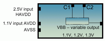
The voltage regulator of Figure 5-31 has three power domains. The power domain associated with the output power supply is referred to as a power source domain.
To model a voltage regulator, you need to use a CPF macro model:
The power source domain must be identified with the
-power_sourceoption in thecreate_power_domain.The power domain of the high input voltage supply must be declared as the base domain (
-base_domains) of the power source domain.Note: The primary supply voltage of the base domain can be different from the voltage of the power source domain.
The options of the
update_power_domaincommand for the power source domain depend on whether the output power supply is used as power source for the primary power supply or body bias supply of other domains:Use the
-primary_power_netoption if the power source can only be used a primary power supply of other domainsUse the
-primary_ground_netoption if the power source is a primary ground supply of other domainsThis occurs when a top design uses the ground bias supply to control the power dissipation and performance and uses the output of the voltage regulator for the ground connection.
Use the
-pmos_bias_netor-nmos_bias_netoption (without the-primary_power_netor-primary_ground_netspecification) if the power source can only be used as body bias supply of other domainsUse the
-primary_power_netand-pmos_bias_netoptions if the power source can be used as a primary power supply and pmos body bias supply of other domainsUse the
-primary_ground_netand-nmos_bias_netoptions if the power source can be used as a primary ground supply and nmos body bias supply of other domains
Note: If the macro has an internal regulator whose output supply only drives logic within the macro, the
update_power_domaincommand for the power source domain will not have any primary power, primary ground, or body bias net specifications. The power source domain is then referred to as an internal power source domain.Specify the reference signal for the power source domain with the
set_power_source_reference_pincommand.In any power mode definition, the nominal condition for the power source domain should have a lower voltage range than the nominal condition for its base domain.
Examples 5-31 through 5-31 apply to Figure 5-31.
Example 5-1 Voltage Regulator Model for Output Power Supply Used as PMOS Body Bias Supply
Power supply VBB will be used as the PMOS body bias supply of top-level domain PDDVFS.
set_macro_model regulator
create_power_domain -name PDVIN
update_power_domain -name PDVIN -primary_power_netHAVDD-primary_ground_net AVSS
create_power_domain -name PDVOUT-default -base_domains {PDVIN} -power_sourceupdate_power_domain -name PDVOUT-pmos_bias_net VBBcreate_power_domain -name PDREF -boundary_ports {C1 C2}
update_power_domain -name PDREF -primary_power_net AVDD -primary_ground_net AVSS
...set_power_source_reference_pin AVDD -domain PDVOUT voltage_range 1.0:1.1end_macro_model regulator
set_design top
create_power_domain -name PDDefault -default
update_power_domain -name PDDefault -primary_power_net AVDD \
-primary_ground_net AVSS
create_power_domain -name PDDirty
update_power_domain -name PDDirty -primary_power_net HighVdd \
-primary_ground_net VSS
create_power_domain -name PDDVFS -instances ...
update_power_domain -name PDDVFS -primary_power_net VDD -primary_ground_net VSS \
-pmos_bias_net VBB-nmos_bias_net VSS0
set_instance I_regulator -domain_mapping { {PDVIN PDDirty} {PDREF PDDefault} \
{PDVOUT PDDVFS}}
....
Example 5-2 Voltage Regulator Model for Output Power Supply Used as PMOS Body Bias Supply with Voltage Range Specification
In this example, the CPF contains voltage ranges for the nominal condition of the power source domain but does not specify how the output voltage is controlled. The simulation model could contain the output voltage behavior.
set_macro_model regulator
create_power_domain -name PDVIN
update_power_domain -name PDVIN -primary_power_net HAVDD -primary_ground_net AVSS
create_power_domain -name PDVOUT -default -base_domains {PDVIN} -power_source
update_power_domain -name PDVOUT -pmos_bias_net VBB
create_power_domain -name PDREF -boundary_ports {C1 C2}
update_power_domain -name PDREF -primary_power_net AVDD -primary_ground_net AVSScreate_nominal_condition -name LDO_range -voltage 1.1 -pmos_bias_voltage 1.1:1.3set_power_source_reference_pin AVDD -domain PDVOUT voltage_range 1.1:1.1
create_nominal_condition -name HVDD -voltage 2.45:2.55 -ground_voltage 0.0
create_nominal_condition -name REF -voltage 1.1 -ground_voltage 0.0
create_power_mode -name PM -default -domain_conditions \
{ PDREF@REF PDVIN@HVDD PDVOUT@LDO_range }
end_macro_model regulator
Example 5-3 Voltage Regulator Model for Output Power Supply Used as PMOS Body Bias Supply with Voltage Control Specification
In this example, the CPF does specify how the output voltage is controlled.
VBB=1.1v when C1=1, C2=0; VBB=1. 2v when C1=0, C2=1; VBB=1. 3v when C1=1, C2=1
set_macro_model regulator create_nominal_condition -name LDO1 -voltage 1.1 -pmos_bias_voltage 1.1create_nominal_condition -name HVDD -voltage 2.5 -ground_voltage 0.0
create_nominal_condition -name LDO2 -voltage 1.1 -pmos_bias_voltage 1.2
create_nominal_condition -name LDO3 -voltage 1.1 -pmos_bias_voltage 1.3
create_nominal_condition -name REF -voltage 1.1 -ground_voltage 0.0
create_power_domain -name PDVIN
update_power_domain -name PDVIN -primary_power_net HAVDD -primary_ground_net AVSS
create_power_domain -name PDVOUT -default -base_domains {PDVIN} -power_source \
-active_state_conditions { LDO1@"C1&!C2" LDO2@"!C1&C2" LDO3@"C1&C2" }update_power_domain -name PDVOUT -pmos_bias_net VBB
create_power_domain -name PDREF -boundary_ports {C1 C2}
update_power_domain -name PDREF -primary_power_net AVDD -primary_ground_net AVSScreate_power_mode -name PM1 -default -domain_conditions \set_power_source_reference_pin AVDD -domain PDVOUT voltage_range 1.1:1.1
{ PDREF@REF PDVIN@HVDD PDVOUT@LDO1 }
create_power_mode -name PM2 -domain_conditions \
{ PDREF@REF PDVIN@HVDD PDVOUT@LDO2 }
create_power_mode -name PM3 -domain_conditions \
{ PDREF@REF PDVIN@HVDD PDVOUT@LDO3 }
end_macro_model regulator
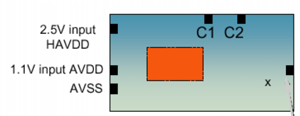
Example 5-4 Macro Cell with an Internal Regulator
The macro below has an internal power regulator. The macro has no pin to export the internal power supply. Some output data pins are driven by logic that are in tern driven by the internal supply.
Figure 5-32 Internal Voltage Regulator
set_macro_model regulator
create_power_domain -name PDVIN
update_power_domain -name PDVIN -primary_power_net HAVDD -primary_ground_net AVSS
create_power_domain -name PDVOUT -default -base_domains {PDVIN}-power_sourcecreate_power_domain -name PDREF -boundary_ports {C1 C2}
update_power_domain -name PDREF -primary_power_net AVDD -primary_ground_net AVSS
create_nominal_condition -name OUT -voltage 0.9:1.1
create_nominal_condition -name HDVV -voltage 2.5 -ground_voltage 0.0
create_nominal_condition -name REF -voltage 1.1 -ground_voltage 0.0
create_power_mode -name PM -default -domain_conditions \
{ PDREF@REF PDVIN@HVDD PDVOUT@OUT }
set_power_source_reference_pin AVDD -domain PDVOUT voltage_range 1.1:1.1
end_macro_model regulator
Power source domain PDVOUT has no update_power_domain command that contains any primary power, primary ground, or body bias net specifications.
Power Domain Mapping of a Power Source Domain
There are special semantics for power domain mapping in case of a power source domain,
The top-level domain inherits all the attributes related to the macro model power source domain:
The top-level domain uses the power ports of a power source domain as either primary supply or body bias supply depending on the specification in the macro model
If the top-level domain already has a shutoff condition specified, it must be functionally equivalent to the conditions specified for the power source domain and the domain must be an external switchable domain.
If the top-level domain also has active state conditions specified, it must be functionally equivalent to the corresponding condition specified for the power source domain.
A power source domain can be mapped into multiple top-level domains.
These top-level domains must have consistent nominal conditions in all power modes
It is an error if multiple power source domains are mapped into the same top-level domain.
The top-level domain's voltage range (specified across all power modes) must be within the voltage range specified with the power source domain.
Depending on the definition and usage of the regulator output port, the top-level domain's nominal operating voltages can be any of the following: power voltage, ground voltage, pmos bias voltage, or nmos bias voltage, or a combination of these. For example, if a regulator output port is defined as a pmos bias supply, then among all power mode definitions for the corresponding top level domain, its pmos bias voltage must be within the range of the operating voltage of the corresponding power source domain.
If a power source domain is switchable, and if the top-level domain it is mapped to is an unswitched domain, the top-level domain becomes switchable with the shutoff condition specified in the macro model using the cell pins. It is an error if a switchable power source domain is mapped into a top-level internal switchable domain.
If a power domain is an internal power source domain, the domain cannot be mapped. The update_power_domain command for the power source domain will not have any primary power, primary ground, or body bias port specifications.
Simulation Semantic
In simulation a power source domain is considered to be corrupted if
Its base domain is off or operates out of the required voltage ranges
Its reference pin is corrupted or operates out of the specified voltage ranges
When a power source domain is corrupted, the power domains mapped to this power source domain are corrupted as well. The corruption semantics applies recursively to all domain mappings that root from the power source domain.