Hierarchical Flow
Introduction to Hierarchical Flow
In Chapter 2, "Creating a CPF File," you learned about the CPF constructs to describe three of the most used low power techniques in a non-hierarchical flow. In this chapter, you will learn more about the additional constructs you need to use for a bottom-up hierarchical flow.
Typically in a bottom-up hierarchical flow, the design instantiates IPs.
If an IP is designed or implemented with a complex power structure, the IP will have a separate CPF file to describe its power intent.
CPF distinguishes the following categories:
A hard non-custom IP is a block that has been synthesized and placed and routed, but small modifications can still be made. It is also referred to as a hard IP.
A hard custom IP is a block that is mostly implemented by hand. Custom IP users cannot make any changes to the block. Examples are third-party memories. A hard custom IP is also referred to as a macro cell.
A soft IP is a design module that can be supplied by a third-party. Users have the full capability to (re-)synthesize and place and route the design. Examples are synthesizable CPU cores, and so on.
When the IP is instantiated at the top level, power domain mapping is required to indicate which power domains from the top-level need to provide power supplies to the IP.
Mapping a power domain of a block (IP) to another power domain at the top level when the block is instantiated in the top-level design involves
Connecting the primary power and ground pins or nets of the block-level domain to the primary power and ground net of the domain specified at the top level
Merging the elements of the power domain of the block into the top-level domain
Resolving the precedence of the top-level and block-level rules
Once a block-level power domain is mapped into a top-level power domain, the two power domains are considered identical and all instances of the two domains share the same power characteristics. For example, the standard cell instances of the two power domains will have their primary power and ground pin (follow pins) connected together to the same primary power and ground nets.
A simplified view of a DTMF receiver, the design used to illustrate the hierarchical flow, is shown in Figure 4-1.
The DTMF receiver design uncompresses and accumulates an eight-bit uLaw encoded dual tone data sampled over a100 millisecond period into a dual buffer memory.
Once an entire sample has been received embedded DSP (TDSP) cores will read the input buffer and execute a modified discrete Fourier transform (DFT) algorithm to calculate a partial frequency spectrum. Upon completion the DSP cores forward the resulting frequency response data for comparison to values corresponding to DTMF digits. If a match is found the 8 bit ASCII digit is presented at the output of the core.
The voltage of the core is scaled depending on the requested function of the design. If the processing speed is critical a higher voltage is used, if the processing speed is not critical, the voltage is dynamically scaled down together with the clock frequency to save power. For this design we assume that the voltage supply is dynamically controlled external to the chip.
Figure 4-1 Example of Hierarchical Design
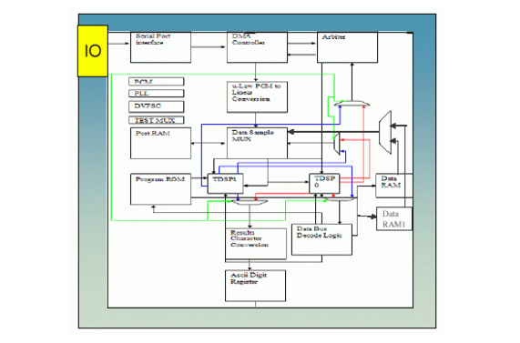
The core of the design is the DTMF_INST instance. The I/O pads are instantiated in a hierarchical instance IOPADS_INST.The DTMF receiver design further contains
A PLL block
This block is used to generate the clocks needed by all the blocks in the design. It has a reference clock,
refclk, that is used to generate all other clocks.Because the design uses two operating voltages, two clock signals are created.
This analog block needs to operate at a constant voltage to ensure correct operation. It therefore needs a dedicated power input,
Avdd.Two TDSP cores:
TDSP0andTDSP1(in Figure 4-1)These two digital signal processing blocks can operate at a higher voltage and frequency, and at a lower voltage and frequency when the processing speed is not critical. When the blocks do not need to be operational, they are powered down.
A
dvfs_ensignal at the input of the chip indicates to thedvfs_controllerwhen the voltage and frequency can be adjusted. The controller sends a signal to the PLL and to the external voltage regulator to adjust the clock frequency and the voltage, respectively.These blocks are instances of the soft block,
tdsp_core. Thetdsp.cpffile describes the power intent of this soft block.Data RAM1is a special RAM that can retain its memory when it is powered down. This RAM can operate at the same voltages as the design core.This RAM is an instance of the hard custom IP,
ram_256x16A. Theram.cpffile describes the power intent of this RAM instance.Data RAMis a regular RAM.This RAM can only operate at one voltage. It can also be powered down when not operational. This RAM does not retain its memory when it is powered down.
The
pm_instblock (not shown in Figure 4-1)
The top-level of the design has the following power domains:
The
PDpllDTMF_INST/PLLCLK_INST) and some of the IO pads (for example,IOPADS_INST/Prefclkip) that are connected to this block.The
PDtdsppower domain contains the two TDSP cores (DTMF_INST/TDSP_CORE_INST0, DTMF_INST/TDSP_CORE_INST1) and the special RAM (DTMF_INST/RAM_128x16_TEST_INST1).The
PDrampower domain contains the regular RAM (DTMF_INST/RAM_128x16_TEST_INST).The
PDshutoff_iopower domain contains two I/O instances that can be powered down.The
PDdefaultpower domain contains all other blocks that do not belong to any special power domain. All these blocks operate in DVFS mode.The
PDram_virtualpower domain contains no blocks.
Power domains PDdefault, PDpll and PDram_virtual are unswitched domains. Power domains PDtdsp, PDram, and PDshutoff_io are switchable domains.
Power domain PDshutoff_io is an on-chip controlled external switchable domain, while power domains PDtdsp and PDram are internal switchable domains; they can be switched off through an internal power switch network. The external power supply for the power switch network of power domain PDtdsp is provided by the power domain PDdefault, while the external power supply for the power switch network of power domain PDram is provided by the power domain PDram_virtual.PDdefault is the secondary power domain for domain PDtdsp, while PDram_virtual is the secondary power domain for domain PDram.
Table 4-1 shows the operating voltages for each of the power domains in the different power modes of the design.
Table 4-1 Voltages of the Power Domains at the Top Level in the Different Power Modes
Table 4-2 shows the different control signals needed at the top-level of the design to isolate logic, turn off the power supply switches, and save and restore the retention states. The always on domains do not need any control signals.
Table 4-2 Signals Controlling the Power Domains at the Top Level
no control signal1 |
|||
| 1 Although no state retention rules are specified at the top-level domain, state retention rules are defined for the special RAM, defined through the ram.cpf (see Macro CPF -- ram.cpf), and for the soft block, defined through the tdsp.cpf (see Soft IP CPF -- tdsp.cpf). |
All control signals are generated by the power control manager (PM_INST) which is an instance of the core.
Table 4-3 lists the operating corners for the design for the corresponding operating voltages.
Table 4-3 Operating Corners
CPF for Hierarchical Flow lists the complete CPF files used for this design.
Steps to Create the CPF File describes the specifics to create a CPF file for a hierarchical flow, assuming your design is using a hard and soft IP for which you have the CPF descriptions.
CPF for Hierarchical Flow
Technology CPF File -- tech.cpf
set_cpf_version 1.1
if { [set_instance] == [set_hierarchy_separator] } {
set libdir ../LIBS/N45GS/timing
set libdir_io ../LIBS/N65LP/timing
#######################################################################
#
#       Technology part of the CPF
#
########################################################################
define_always_on_cell -cells PTBUFFD2BWP \
   	 -power_switchable VDD -power TVDD -ground VSS
define_isolation_cell -cells ISO* \
   	 -power VDD -ground VSS \
   	 -enable ISO \
   	 -valid_location to
define_level_shifter_cell -cells LVL*HLD* \
   	 -input_voltage_range 0.72:0.81:0.09 \
   	 -output_voltage_range 0.72:0.81:0.09 \
   	 -direction down \
   	 -output_power_pin VDD \
   	 -ground VSS \
   	 -valid_location to
define_level_shifter_cell -cells PTLVL*HLD* \
   	 -input_voltage_range 0.72:0.81:0.09 \
   	 -output_voltage_range 0.72:0.81:0.09 \
   	 -direction down \
   	 -output_power_pin TVDD \
   	 -ground VSS \
   	 -valid_location to
define_level_shifter_cell -cells LVLLHCD* \
   	 -input_voltage_range 0.72:0.81:0.09 \
   	 -output_voltage_range 0.72:0.81:0.09 \
   	 -enable NSLEEP \
   	 -input_power_pin VDDL \
   	 -output_power_pin VDD \
   	 -direction up \
   	 -ground VSS \
   	 -enable NSLEEP \
   	 -valid_location to
define_level_shifter_cell -cells LVLLHD* \
   	 -input_voltage_range 0.72:0.81:0.09 \
   	 -output_voltage_range 0.72:0.81:0.09 \
   	 -input_power_pin VDDL \
   	 -output_power_pin VDD \
   	 -direction up \
   	 -ground VSS \
   	 -valid_location to
define_power_switch_cell -cells {HDRDID1BWPHVT HDRDIAOND1BWPHVT} \
   	 -power_switchable VDD -power TVDD \
   	 -stage_1_enable NSLEEPIN1 -stage_1_output NSLEEPOUT1 \
   	 -stage_2_enable NSLEEPIN2 -stage_2_output NSLEEPOUT2 \
   	 -type header
define_state_retention_cell \
   	 -cells {MSRSDFCSNQHD2BWP} \
   	 -cell_type "master_slave" \
   	 -clock_pin CP \
   	 -power TVDD -power_switchable VDD \
   	 -ground VSS \
   	 -restore_check "!CP" \
   	 -save_function "!CP" \
   	 -always_on_components DFF_inst
define_state_retention_cell \
   	 -cells {RSDFCSRHD2BWP} \
   	 -clock_pin CP \
   	 -power TVDD -power_switchable VDD \
   	 -ground VSS \
   	 -save_function "SAVE" \
   	 -cell_type "ballon_latch" \
   	 -restore_function "!NRESTORE" \
   	 -always_on_components save_data
########################################################################
## DEFINE LIBRARY SET
########################################################################
set lib_0v81_wc_base "$libdir/tcbn45gsbwpwc.lib"
set lib_0v81_wc_extra "\
   	 $libdir/tcbn45lpbwp_c070208wc0d720d9_modified.lib \
   	 $libdir/tcbn45lpbwp_c070208wc0d90d9_modified.lib \
   	 $libdir/tcbn45lpbwp_c070208wc_modified.lib \
   	 $libdir/pllclk_slow.lib \
   	 $libdir/ram_256x16A_slow_syn.lib \
   	 $libdir/rom_512x16A_slow_syn.lib "
set lib_0v81_bc_base "$libdir/tcbn45gsbwpbc.lib "
set lib_0v81_bc_extra "\
   	 $libdir/tcbn45lpbwp_c070208bc0d881d1_modified.lib \
   	 $libdir/tcbn45lpbwp_c070208bc1d11d1_modified.lib \
   	 $libdir/tcbn45lpbwp_c070208bc_modified.lib \
   	 $libdir/pllclk_slow.lib \
   	 $libdir/ram_256x16A_slow_syn.lib \
   	 $libdir/rom_512x16A_slow_syn.lib "
set lib_0v72_wc_base "$libdir/tcbn45gsbwpwc_0d72.lib "
set lib_0v72_wc_extra "\
   	 $libdir/tcbn45lpbwp_c070208wc0d90d72_modified.lib \
   	 $libdir/tcbn45lpbwphvt_c070208wc0d72_modified.lib \
   	 $libdir/tcbn45lpbwp_c070208wc0d72_ptlvl_modified.lib \
   	 $libdir/tcbn45lpbwp_c070208wc0d720d72_modified.lib \
   	 $libdir/ram_256x16A_slow_syn.lib \
   	 $libdir/rom_512x16A_slow_syn.lib "
set lib_0v72_bc_base "$libdir/tcbn45gsbwpbc_0d88.lib "
set lib_0v72_bc_extra "\
   	 $libdir/tcbn45lpbwp_c070208bc1d10d88_modified.lib \
   	 $libdir/tcbn45lpbwphvt_c070208bc0d88_modified.lib \
   	 $libdir/tcbn45lpbwp_c070208bc0d88_ptlvl_modified.lib \
   	 $libdir/tcbn45lpbwp_c070208bc0d880d88_modified.lib \
   	 $libdir/ram_256x16A_fast_syn.lib \
   	 $libdir/rom_512x16A_slow_syn.lib "
set io_lib_wc "$libdir_io/tpzn65lpgv2wc.lib"
set io_lib_bc "$libdir_io/tpzn65lpgv2bc.lib"
define_library_set -name wc_0v81 -libraries "$lib_0v81_wc_base \
   	 $lib_0v81_wc_extra $io_lib_wc"
define_library_set -name bc_0v81 -libraries "$lib_0v81_bc_base \
   	 $lib_0v81_bc_extra $io_lib_bc"
define_library_set -name wc_0v72 -libraries "$lib_0v72_wc_base \
   	 $lib_0v72_wc_extra $io_lib_wc"
define_library_set -name bc_0v72 -libraries "$lib_0v72_bc_base \
   	 $lib_0v72_bc_extra $io_lib_wc"
}
Top CPF File
set_cpf_version 1.1
set_hierarchy_separator /
set_design dtmf_chip
set constraintDir $env(test_PATH)/RELEASE/mmmc
include tech.cpf
########################################################################
## create power domains
########################################################################
create_power_domain -name PDdefault-default
update_power_domain -name PDdefault -primary_power_net VDD -primary_ground_net VSS
create_power_domain -name PDshutoff_io\
-instances {IOPADS_INST/Pspifsip IOPADS_INST/Pspidip} \
-boundary_ports {spi_fs spi_data} \
-shutoff_condition {io_shutoff_ack} \
-external_controlled_shutoff
update_power_domain -name PDshutoff_io -primary_power_net VDD_IO \
   	 -primary_ground_net VSS
create_power_domain -name PDpll\
-instances {DTMF_INST/PLLCLK_INST \
IOPADS_INST/Pibiasip \
IOPADS_INST/Ppllrstip \
IOPADS_INST/Prefclkip \
IOPADS_INST/Pvcomop \
IOPADS_INST/Pvcopop} \
-boundary_ports { ibias reset refclk vcom vcop pllrst }
update_power_domain -name PDpll -primary_power_net Avdd -primary_ground_net Avss
create_power_domain -name PDram_virtual
update_power_domain -name PDram_virtual -primary_power_net VDDL \
   	 -primary_ground_net VSS
create_power_domain -name PDram\
-shutoff_condition {!DTMF_INST/PM_INST/power_switch_enable} \
-base_domains PDram_virtual \
-instances DTMF_INST/RAM_128x16_TEST_INST
update_power_domain -name PDram -primary_power_net VDDL_sw -primary_ground_net VSS
create_power_domain -name PDtdsp\
-shutoff_condition {!DTMF_INST/PM_INST/power_switch_enable} \
-base_domains PDdefault
update_power_domain -name PDtdsp -primary_power_net VDD_sw -primary_ground_net VSS
########################################################################
## create power modes
########################################################################
create_nominal_condition -name nom_0v81 -voltage 0.81
update_nominal_condition -name nom_0v81 -library_set wc_0v81
create_nominal_condition -name nom_0v72 -voltage 0.72
update_nominal_condition -name nom_0v72 -library_set wc_0v72
create_power_mode -name PMdvfs1\
-domain_conditions {PDpll@nom_0v81 PDdefault@nom_0v81 PDtdsp@nom_0v81 \
PDram@nom_0v72 PDshutoff_io@nom_0v81 \
PDram_virtual@nom_0v72} \
-default
update_power_mode -name PMdvfs1 -sdc_files ${constraintDir}/dtmf_dvfs1.sdc
create_power_mode -name PMdvfs1_off\
-domain_conditions {PDpll@nom_0v81 PDdefault@nom_0v81 PDshutoff_io@nom_0v81 \
PDram_virtual@nom_0v72}
create_power_mode -name PMdvfs1_shutoffio_off\
-domain_conditions {PDpll@nom_0v81 PDdefault@nom_0v81 PDram_virtual@nom_0v72}
create_power_mode -name PMdvfs2\
-domain_conditions {PDpll@nom_0v81 PDdefault@nom_0v72 PDtdsp@nom_0v72 \
PDram@nom_0v72 PDshutoff_io@nom_0v72 \
PDram_virtual@nom_0v72}
update_power_mode -name PMdvfs2 -sdc_files ${constraintDir}/dtmf_dvfs2.sdc
create_power_mode -name PMdvfs2_off\
-domain_conditions {PDpll@nom_0v81 PDdefault@nom_0v72 PDshutoff_io@nom_0v72 \
PDram_virtual@nom_0v72}
create_power_mode -name PMdvfs2_shutoffio_off\
-domain_conditions {PDpll@nom_0v81 PDdefault@nom_0v72 PDram_virtual@nom_0v72}
create_power_mode -name PMscan\
-domain_conditions {PDpll@nom_0v81 PDdefault@nom_0v81 PDtdsp@nom_0v81 \
PDram@nom_0v72 PDshutoff_io@nom_0v81 PDram_virtual@nom_0v72}
update_power_mode -name PMscan -sdc_files ${constraintDir}/dtmf_scan.sdc
########################################################################
## domain mapping
########################################################################
set_instance DTMF_INST/TDSP_CORE_INST0 \
   	 -domain_mapping { {PDtdsp_block PDtdsp} } \
   	 -port_mapping { {retention_save DTMF_INST/PM_INST/state_retention_save} \
   	    	    	    	 {retention_restore DTMF_INST/PM_INST/state_retention_restore} }
include tdsp.cpf
set_instance DTMF_INST/TDSP_CORE_INST1 \
   	 -domain_mapping { {PDtdsp_block PDtdsp} } \
   	 -port_mapping { {retention_save DTMF_INST/PM_INST/state_retention_save} \
   	    	    	    	 {retention_restore DTMF_INST/PM_INST/state_retention_restore} }
include tdsp.cpf
set_instance DTMF_INST/RAM_128x16_TEST_INST1/RAM_128x16_INST \
   	 -domain_mapping { {RAM_DEFAULT PDtdsp} }
include ram.cpf
########################################################################
## create isolation and level shifter rules
########################################################################
create_isolation_rule -name ISORULE1 \
   	 -from PDtdsp \
   	 -to PDdefault \
   	 -isolation_condition {!DTMF_INST/PM_INST/isolation_enable} \
   	 -isolation_output high
create_isolation_rule -name ISORULE3 \
   	 -from PDram \
   	 -to PDdefault \
   	 -isolation_condition {!DTMF_INST/PM_INST/isolation_enable} \
   	 -isolation_output high
create_isolation_rule -name ISORULE4  \
   	 -from PDshutoff_io \
   	 -isolation_condition {!DTMF_INST/PM_INST/spi_ip_isolate} \
   	 -isolation_output low
create_level_shifter_rule -name LSRULE_H2L3 \
   	 -from PDdefault \
   	 -to  PDram \
   	 -exclude { DTMF_INST/PM_INST/power_switch_enable }
update_level_shifter_rules -names LSRULE_H2L3 -location to -cells LVLHLD2BWP
create_level_shifter_rule -name LSRULE_H2L3_SW \
   	 -from PDdefault \
   	 -to  PDram \
   	 -pins { DTMF_INST/PM_INST/power_switch_enable }
update_level_shifter_rules -names LSRULE_H2L3_SW \
   	 -location to \
   	 -cells PTLVLHLD2BWP \
   	 -prefix CPF_LS_SW
create_level_shifter_rule -name LSRULE_L2H2  \
   	 -from PDram \
   	 -to   PDdefault
create_level_shifter_rule -name LSRULE_H2L_PLL \
   	 -from PDpll
create_level_shifter_rule -name LSRULE_L2H3
   	 -from PDdefault   \
   	 -to   PDpll
########################################################################
## create power net
########################################################################
create_power_nets -nets VDD -voltage {0.72:0.81:0.09}
create_power_nets -nets VDD_sw -internal -voltage {0.72:0.81:0.09}
create_power_nets -nets VDDL -voltage 0.72
create_power_nets -nets VDDL_sw -internal -voltage 0.72
create_power_nets -nets Avdd -voltage 0.81
create_power_nets -nets VDD_IO -voltage {0.72:0.81:0.09} \
   	 -external_shutoff_condition {io_shutoff_ack}
create_ground_nets -nets Avss -voltage 0
create_ground_nets -nets VSS -voltage 0
########################################################################
## create analysis view
########################################################################
create_operating_corner -name PMdvfs2_bc \
   	 -process 1 -temperature 0 -voltage 0.88  \
   	 -library_set bc_0v72
create_operating_corner -name PMdvfs1_bc \
   	 -process 1 -temperature 0 -voltage 0.99 \
   	 -library_set bc_0v81
create_operating_corner -name PMdvfs1_wc \
   	 -process 1 -temperature 125 -voltage 0.81 \
   	 -library_set wc_0v81
create_operating_corner -name PMdvfs2_wc \
   	 -process 1 -temperature 125 -voltage 0.72 \
   	 -library_set wc_0v72
create_analysis_view -name AV_dvfs1_BC -mode PMdvfs1    \
   	 -domain_corners {PDpll@PMdvfs1_bc PDdefault@PMdvfs1_bc PDtdsp@PMdvfs1_bc \
   	    	    	    	    	 PDram@PMdvfs2_bc PDshutoff_io@PMdvfs1_bc}
create_analysis_view -name AV_dvfs1_WC -mode PMdvfs1 \
   	 -domain_corners {PDpll@PMdvfs1_wc PDdefault@PMdvfs1_wc PDtdsp@PMdvfs1_wc \
   	    	    	    	    	 PDram@PMdvfs2_wc PDshutoff_io@PMdvfs1_wc}
create_analysis_view -name AV_dvfs1_off_BC -mode PMdvfs1_off \
   	 -domain_corners {PDpll@PMdvfs1_bc PDdefault@PMdvfs1_bc \
   	    	    	    	    	 PDshutoff_io@PMdvfs1_bc}
create_analysis_view -name AV_dvfs1_off_WC -mode PMdvfs1_off \
   	 -domain_corners {PDpll@PMdvfs1_wc PDdefault@PMdvfs1_wc \
   	    	    	    	    	 PDshutoff_io@PMdvfs1_wc}
create_analysis_view -name AV_dvfs1_shutoffio_off_BC -mode PMdvfs1_shutoffio_off \
   	 -domain_corners {PDpll@PMdvfs1_bc PDdefault@PMdvfs1_bc}
create_analysis_view -name AV_dvfs1_shutoffio_off_WC -mode PMdvfs1_shutoffio_off \
   	 -domain_corners {PDpll@PMdvfs1_wc PDdefault@PMdvfs1_wc}
create_analysis_view -name AV_dvfs2_BC -mode PMdvfs2 \
   	 -domain_corners {PDpll@PMdvfs1_bc PDdefault@PMdvfs2_bc PDtdsp@PMdvfs2_bc \
   	    	    	    	    	 PDram@PMdvfs2_bc PDshutoff_io@PMdvfs2_bc}
create_analysis_view -name AV_dvfs2_WC -mode PMdvfs2 \
   	 -domain_corners {PDpll@PMdvfs1_wc PDdefault@PMdvfs2_wc PDtdsp@PMdvfs2_wc \
   	    	    	    	    	 PDram@PMdvfs2_wc PDshutoff_io@PMdvfs2_wc}
create_analysis_view -name AV_PMdvfs2_off_BC -mode PMdvfs2_off \
   	 -domain_corners {PDpll@PMdvfs1_bc PDdefault@PMdvfs2_bc \
   	    	    	    	    	 PDshutoff_io@PMdvfs2_bc}
create_analysis_view -name AV_PMdvfs2_off_WC -mode PMdvfs2_off \
   	 -domain_corners {PDpll@PMdvfs1_wc PDdefault@PMdvfs2_wc \
   	    	    	    	    	 PDshutoff_io@PMdvfs2_wc}
create_analysis_view -name AV_dvfs2_shutoffio_off_BC -mode PMdvfs2_shutoffio_off \
   	 -domain_corners {PDpll@PMdvfs1_bc PDdefault@PMdvfs2_bc}
create_analysis_view -name AV_dvfs2_shutoffio_off_WC -mode PMdvfs2_shutoffio_off \
   	 -domain_corners {PDpll@PMdvfs1_wc PDdefault@PMdvfs2_wc}
create_analysis_view -name AV_scan_BC -mode PMscan \
   	 -domain_corners {PDpll@PMdvfs1_bc PDdefault@PMdvfs1_bc PDtdsp@PMdvfs1_bc \
   	    	    	    	    	 PDram@PMdvfs2_bc PDshutoff_io@PMdvfs1_bc}
create_analysis_view -name AV_scan_WC -mode PMscan \
   	 -domain_corners {PDpll@PMdvfs1_wc PDdefault@PMdvfs1_wc PDtdsp@PMdvfs1_wc\
   	    	    	    	    	 PDram@PMdvfs2_wc PDshutoff_io@PMdvfs1_wc}
########################################################################
##power switch, level shifter, isolation cell
########################################################################
create_power_switch_rule -name PDram_SW -domain PDram -external_power_net VDDL
update_power_switch_rule -name PDram_SW \
   	 -cells HDRDID1BWPHVT \
   	 -prefix CDN_SW_RAM
create_power_switch_rule -name PDtdsp_SW -domain PDtdsp -external_power_net VDD
update_power_switch_rule -name PDtdsp_SW \
   	 -cells HDRDID1BWPHVT \
   	 -prefix CDN_SW_TDSP
end_design
Macro CPF -- ram.cpf
set_cpf_version 1.1
set_macro_model ram_256x16A
# This is a special RAM that retains its memory when it is powered down
# RAM has one power domain
create_power_domain -name RAM_DEFAULT -default \
   	 -boundary_ports {A* D* CLK CEN WEN Q*}
update_power_domain -name RAM_DEFAULT -primary_power_net VDD \
   	 -primary_ground_net VSS
# incomplete iso rule specified: the required iso value at inputs
# when driving domain is off
create_isolation_rule -name RAM_iso -isolation_output high -to RAM_DEFAULT
   	 -pins {A* D* CLK CEN WEN}
create_state_retention_rule -name RAM_ret -instances mem* -save_edge !CLK
end_macro_model
Soft IP CPF -- tdsp.cpf
set_cpf_version 1.1
set_design tdsp_core -ports { retention_save retention_restore }
include tech.cpf
########################################################################
## create power domains
########################################################################
create_power_domain -name PDtdsp_block -default
update_power_domain -name PDtdsp_block -primary_power_net VDDtdsp_SW \
   	 -primary_ground_net VSStdsp
create_nominal_condition -name nom_0v72 -voltage 0.72
update_nominal_condition -name nom_0v72 -library_set wc_0v72
create_nominal_condition -name off -voltage 0
create_isolation_rule -name PDtdsp_iso -to PDtdsp_block -isolation_output low
########################################################################
## create power modes
########################################################################
create_power_mode -name PMtdsp_ON \
   	 -domain_conditions {PDtdsp_block@nom_0v72} \
   	 -default
create_power_mode -name PMtdsp_OFF \
   	 -domain_conditions {PDtdsp_block@off}
########################################################################
## low power rules
########################################################################
create_state_retention_rule -name PDtdsp_retention_rule \
   	 -domain PDtdsp_block  -save_edge retention_save \
   	 -restore_edge {!retention_restore}
update_state_retention_rules -names PDtdsp_retention_rule \
   	 -cell_type "ballon_latch"
end_design
Steps to Create the CPF File
Note: The example shown in Figure 4-1 is used throughout this section.
Understanding the CPF file of the Macro Cell
A macro cell can have a behavioral model to describe its functionality. Implementation and verification tools therefore have to rely on the CPF modeling of the internal power network using the boundary ports. This section shows some of the constructs you can expect in a CPF macro model.
For the complete CPF macro model used in this design, refer to Macro CPF -- ram.cpf.
The definition of a CPF macro model starts with a
set_macro_modelcommand that specifies the name of the library cell that represents the macro cell.For the macro model used in the design in Figure 4-1:
The definition ends with an
end_macro_modelcommand.The CPF macro model lists all the power domains that the macro cell contains.
Only the (boundary) input and output pins of the macro cell are visible to the outside world. The input and output pins that belong to a specific power domain are specified through the
-boundary_portsoption of the correspondingcreate_power_domaincommand.The domain definition indicates whether the domain is always on or switchable. For switchable domains, the definition also indicates how the domain is powered down.
The CPF macro model used in the design in Figure 4-1 has one power domain. All of its boundary pins belong to this domain. The power domain is further unswitched.
The CPF macro model also specifies for each of its power domains the boundary ports that provide the power supply to that domain.
For the CPF macro model used in the design in Figure 4-1:
If the macro cell has switchable power domains, its CPF macro model can contain isolation rules.
A complete isolation rule in a macro cell describes the isolation logic implemented inside the macro cell. Complete rules contain the isolation condition and isolation output. Complete rules are optional but can be specified for documentation purposes.
IP blocks can have special requirements for input ports. For example, when the domains driving these input ports are switched off, the signals must be held at specific values. For these signals, no isolation condition can be specified because the IP developer has no knowledge of how the IP will be used.
For such cases, isolation rules without enable conditions (neither
-isolation_conditionnor-no_conditionoption specified) are specified. Such isolation rules are called incomplete isolation rules.For the CPF macro model used in the design in Figure 4-1, an incomplete isolation rule specifies the required isolation value at its inputs when the driving domain is powered down.
create_isolation_rule -name RAM_iso -to RAM_DEFAULT -isolation_output low \
   	 -pins {A* D* CLK CEN WEN}
Note: For more information on how incomplete isolation rules are addressed when the macro is used, refer to "Resolve the precedence of the top-level and block-level rules" in Instantiating the Macro Cell in the Top-Level CPF and Loading the Corresponding CPF.
If the macro cell has switchable power domains, the CPF macro model can contain state retention rules.
For the macro cell in Figure 4-1, one state retention rule is defined.
If the macro cell contains several switchable power domains, the CPF macro model can list its power modes. This allows the verification tools to check consistency between the modes defined at the top-level and in the macro to ensure that the macro cell is correctly integrated in the design.
 | Because a macro model is already implemented, there is no need to include a CPF file with technology-related information. |
For more information on macro modeling, refer to Modeling a Macro Cell in the Common Power Format Language Reference.
Understanding the CPF file of the Soft IP
As opposed to a macro cell, the power intent of a soft IP still needs to be implemented. A soft IP can therefore be seen as an independent small design.
For the complete CPF of the soft block used in this design, refer to Soft IP CPF -- tdsp.cpf.
The definition of a soft IP starts with a
set_designcommand that specifies the name of the module that represents the soft IP.If the soft IP requires virtual ports (additional ports that do not exist in the definition of this module before implementation) for the control signals of the low power logic such as isolation logic, state-retention logic, and so on, these ports are specified with the
-portsoption of theset_designcommand.For the soft block used in the design in Figure 4-1:
The definition ends with an
end_designcommand.All commands between
set_designandend_designdescribe the internal power intent of the soft IP.The constructs used depend on the low power technique used. For more information, see the Chapter 2, "Creating a CPF File."
Creating the CPF File for the Top-Level Design
The CPF of the top-level design contains the following information:
Definition of the power domains at the top level
Definition of the nominal conditions at the top level
Definition of the power modes at the top level
Association of the library sets with the nominal conditions
Instantiating the Macro Cell in the Top-Level CPF and Loading the Corresponding CPF
Instantiating a Soft IP in the Top-Level CPF and Loading the Corresponding CPF
Specification of the rules at the top-level
Specification of timing constraints, power targets, switching activities per mode
Declaration of the power and ground nets
Declaration of the global connections
Addition of implementation information to the rules
Specification of the operating corners
Specification of the analysis views
The steps shown in bold are unique to the hierarchical flow and will be further explained here.
For the complete CPF of the top-level design in Figure 4-1, refer to Top CPF File.
Instantiating the Macro Cell in the Top-Level CPF and Loading the Corresponding CPF
When you instantiate a macro cell in the design, you must indicate which CPF macro model applies to the specified instance. This can be done in one of the following ways:
First load the CPF macro model, then use the
set_instancecommand with the-modeloption to reference the CPF macro model.Explicitly (see Example 4-1)
Implicitly using the
includecommand (see Example 4-2)
Use the
set_instancecommand without the-modeloption, immediately followed by the CPF macro model.Explicitly (see Example 4-3)
Implicitly using the
includecommand (see Example 4-4)
Example 4-1 Explicit CPF Specification of Macro Loaded before Macro Instantiation
set_macro_modelram_256x16A
...end_macro_model
set_design dtmf_chip
create_power_domain ...
create_nominal_condition ...
update_nominal_condition ...
create_power_mode...
set_instanceDTMF_INST/RAM_128x16_TEST_INST1/RAM_128x16_INST-modelram_256x16A \
-domain_mapping { {RAM_DEFAULT PDtdsp} }
...
end_design
Example 4-2 Implicit CPF Specification of Macro Loaded before Macro Instantiation
includeram.cpf
set_design dtmf_chip
create_power_domain ...
create_nominal_condition ...
update_nominal_condition ...
create_power_mode...
set_instanceDTMF_INST/RAM_128x16_TEST_INST1/RAM_128x16_INST-modelram_256x16A \
-domain_mapping { {RAM_DEFAULT PDtdsp} }
...
end_design
Example 4-3 Explicit CPF Specification of Macro Loaded after Macro Instantiation
set_design dtmf_chip
create_power_domain ...
create_nominal_condition ...
update_nominal_condition ...
create_power_mode...
set_instanceDTMF_INST/RAM_128x16_TEST_INST1/RAM_128x16_INST \
-domain_mapping { {RAM_DEFAULT PDtdsp} }set_macro_modelram_256x16A
...
end_macro_model
...
end_design
Example 4-4 Implicit CPF Specification of Macro Loaded after Macro Instantiation
set_design dtmf_chip
create_power_domain ...
create_nominal_condition ...
update_nominal_condition ...
create_power_mode...
set_instanceDTMF_INST/RAM_128x16_TEST_INST1/RAM_128x16_INST \
-domain_mapping { {RAM_DEFAULT PDtdsp} }
includeram.cpf
...
end_design
When you instantiate a macro cell in the design, you must also indicate how the domains of the CPF macro model must be mapped to the domains of the parent level using the -domain_mapping option of the set_instance command. For the example in Figure 4-1:
set_instance DTMF_INST/RAM_128x16_TEST_INST1/RAM_128x16_INST \
   	 -domain_mapping { {RAM_DEFAULT PDtdsp} }
The ram_256x16A model contains one power domain, RAM_DEFAULT. The set_instance command indicates that this domain must be mapped to the PDtdsp domain.
By mapping the domains, the tools will be able to
Connect the primary power and ground pins of the block-level domain to the primary power and ground nets of the corresponding domain specified at the top level.
The primary power and ground pins of power domain
RAM_DEFAULTareVDDandVSS, while the primary nets of power domainPDtdspareVDDL_swandVSS. This implies thatVDDwill be connected toVDDL_sw, while theVSSpin will be connected to theVSSnet.Merge the elements of each block-level domain into the corresponding top-level domain.
Merge the power modes of the CPF macro model with the power modes of the top level.
In this design, the
ram_256x16Amodel does not have a power mode defined, it will have the same power modes as the top-level domainPDtdsp.Resolve the precedence of the power domain settings.
Power domain settings are also referred to as domain attributes. For more information, refer to Handling Domain Attributes after Domain Mapping in the Common Power Format Language Reference. In this design there are no domain attributes to be resolved.
Resolve the precedence of the top-level and block-level rules.
The top-level domain
PDtdsphas no state retention rules. Even if the domain did have a rule, the block-level rule would still overwrite the top-level rule.The CPF macro model used in this design also has an isolation rule.
The isolation rule
RAM_isois an incomplete rule and applies to the net segments that drive logic in theRAM_DEFAULTdomain. It also requires that the output value of the isolation gates be low when isolation is in effect. The rule specifies the isolation requirements at the selected ports of the macro and this information can be used by the top-level CPF to generate the correct isolation rule at this port.The tools will check the power domain to which the leaf level driver of a net selected by the rule belongs.
If the leaf-level driver belongs to the same power domain as the port that the rule applies to, or an unswitched power domain, no isolation of that net segment is needed.
If the leaf-level driver belongs to a different switchable power domain, the tools will check if that power domain has a default isolation condition. If a default isolation condition is defined, this condition can be used by the incomplete isolation rule to make the rule complete. If no default isolation condition was defined for the driving power domain, the incomplete isolation rule is treated as a design constraint.
Instantiating a Soft IP in the Top-Level CPF and Loading the Corresponding CPF
When you instantiate a soft block in the design, you must indicate which CPF specification applies to the specified instance. This can be done in one of the following ways:
First load the CPF specification, then use the
set_instancecommand with the-designoption.Explicitly (see Example 4-5)
Implicitly using the
includecommand (see Example 4-6)
Use the
set_instancecommand without the-designoption, followed by the CPF specification.Explicitly (see Example 4-7)
Implicitly using the
includecommand (see Example 4-8)
Example 4-5 Explicit CPF Specification of Soft IP Loaded before Soft IP Instantiation
set_designtdsp_core -ports { retention_save retention_restore }
...
end_design
set_design dtmf_chip
create_power_domain ...
create_nominal_condition ...
update_nominal_condition ...
create_power_mode...
set_instanceDTMF_INST/TDSP_CORE_INST0-designtdsp_core \
-domain_mapping { {PDtdsp_block PDtdsp} } \
-port_mapping { {retention_save DTMF_INST/PM_INST/state_retention_save} \
{retention_restore DTMF_INST/PM_INST/state_retention_restore} }
...
end_design
Example 4-6 Implicit CPF Specification of Soft IP Loaded before Soft IP Instantiation
includetdsp.cpf
set_design dtmf_chip
create_power_domain ...
create_nominal_condition ...
update_nominal_condition ...
create_power_mode...
set_instanceDTMF_INST/TDSP_CORE_INST0-designtdsp_core \
-domain_mapping { {PDtdsp_block PDtdsp} } \
-port_mapping { {retention_save DTMF_INST/PM_INST/state_retention_save} \
{retention_restore DTMF_INST/PM_INST/state_retention_restore} }
...
end_design
Example 4-7 Explicit CPF Specification of Soft IP Loaded after Soft IP Instantiation
set_design dtmf_chip
create_power_domain ...
create_nominal_condition ...
update_nominal_condition ...
create_power_mode...
set_instanceDTMF_INST/TDSP_CORE_INST0 -domain_mapping { {PDtdsp_block PDtdsp} } \
-port_mapping { {retention_save DTMF_INST/PM_INST/state_retention_save} \
{retention_restore DTMF_INST/PM_INST/state_retention_restore} }
set_designtdsp_core -ports { retention_save retention_restore }
... end_design
...
end_design
Example 4-8 Implicit CPF Specification of Soft IP Loaded after Soft IP Instantiation
set_design dtmf_chip
create_power_domain ...
create_nominal_condition ...
update_nominal_condition ...
create_power_mode...
set_instanceDTMF_INST/TDSP_CORE_INST0 -domain_mapping { {PDtdsp_block PDtdsp} } \
-port_mapping { {retention_save DTMF_INST/PM_INST/state_retention_save} \
{retention_restore DTMF_INST/PM_INST/state_retention_restore} }
includetdsp.cpf
...
end_design
When you instantiate a soft block in the design, you must also indicate
How the domains of the soft block must be mapped to the domains of the parent level using the
-domain_mappingoption of theset_instancecommand.How the virtual ports must be mapped to the parent-level drivers using the
-port_mappingoption of theset_instancecommand. If there are no virtual ports declared in the correspondingset_designcommand, this option is not needed.The values that must be assigned to the parameters declared in the block-level CPF using the
-parameter_mappingoption of theset_instancecommand. If there are no parameters declared in the correspondingset_designcommand, this option is not needed.Note: For an example of parameter mapping, see the Examples for the
set_instancecommand.
The example in Figure 4-1 has two instances of the same soft block:
set_instance DTMF_INST/TDSP_CORE_INST0 \
-domain_mapping{ {PDtdsp_block PDtdsp} } \
-port_mapping{ {retention_save DTMF_INST/PM_INST/state_retention_save} \
{retention_restore DTMF_INST/PM_INST/state_retention_restore} }
set_instance DTMF_INST/TDSP_CORE_INST1 \
-domain_mapping{ {PDtdsp_block PDtdsp} } \
-port_mapping{ {retention_save DTMF_INST/PM_INST/state_retention_save} \
{retention_restore DTMF_INST/PM_INST/state_retention_restore} }
The tdsp_core model contains only one power domain, PDtdsp_block, which is mapped to the PDtdsp power domain for both instances. The two virtual ports for state retention control signals are connected to two output pins of the power control module (PM_INST).
The PDtdsp_block domain is an external switchable block-level domain, so it can be mapped into any type of domain at the top level. For other cases of domain mapping, refer to Handling Power Domain Mapping in the Common Power Format Language Reference.
By mapping the domains, the tools will be able to
Connect the primary power and ground nets of the block-level domain to the primary power and ground nets of the corresponding domain specified at the top level.
The primary power and ground nets of power domain
PDtdsp_blockareVDDtdsp_SWandVSStdsp, while the primary nets of power domainPDtdspareVDDL_swandVSS. This implies thatVDDtdsp_SWwill be connected toVDDL_sw, whileVSStdspwill be connected to theVSSnet.Merge the elements of each block-level domain into the corresponding top-level domain.
Because the soft block In this design only has one block domain, the
TDSP_CORE_INST0andTDSP_CORE_INST1instances becomes instances of thePDtdspdomain.Merge the power modes of the soft IP with the power modes of the top level.
If all block-level domains are mapped into top-level domains, the top-level mode definitions also become the power modes for the soft block after the domain mapping.
In this design, the
tdsp_coremodel has two power modes defined. Because it's one power domain maps to a top-level power domain, the soft block will have the same power modes as the top-level domainPDtdsp.For more information, refer to Handling Power Modes after Domain Mapping in the Common Power Format Language Reference.
Resolve the precedence of the power domain settings.
Power domain settings are also referred to as domain attributes. For more information, refer to Handling Domain Attributes after Domain Mapping in the Common Power Format Language Reference. In this design there are no domain attributes to be resolved.
Resolve the precedence of the top-level and block-level rules.
create_state_retention_rule -name PDtdsp_retention_rule \
   	 -domain PDtdsp_block  -save_edge retention_save \
   	 -restore_edge {!retention_restore}
The top-level domain
PDtdsphas no state retention rules. Even if the domain did have a rule, the block-level rule would still overwrite the top-level rule.The CPF specification of the soft IP used in this design also has an isolation rule.
The isolation rule
PDtdsp_isois an incomplete rule and applies to the net segments that drive logic in thePDtdsp_blockdomain. It also requires that the output value of the isolation gates be low when isolation is in effect. However to complete the rule, the isolation condition must be derived from the corresponding top-level domain.The tools will check the power domain to which the leaf level driver of a net selected by the rule belongs.
If the leaf-level driver belongs to the same power domain, no isolation of that net segment is needed.
If the leaf-level driver belongs to a different switchable power domain, the tools will check if that power domain has a default isolation condition. If a default isolation condition is defined, this condition can be used by the incomplete isolation rule to make the rule complete. If no default isolation condition was defined for the driving power domain, the incomplete isolation rule is treated as a design constraint.
In this design the IP instances,
TDSP_CORE_INST0andTDSP_CORE_INST1,are driven by leaf-level drivers in thePDdefaultdomain, which is a non-switchable domain.For more information refer to Precedence of Rules in the Hierarchical Flow in the Common Power Format Language Reference