- Overview
- OpenAccess Compatibility for Mixed-Signal STA Flow
- Handling Schematic-Driven Designs Implemented Using a Non-Interoperable PDK
- Running STA by Flattening the Design
- Running STA by Using the FTM
- Difference between Flat and FTM Approaches
- Guidelines for Running STA Flow on Mixed-Signal Design
- Creating a Quick Timing Model for Analog IPs in Innovus
- Different Ways of Running assembleDesign
- Running assembleDesign in the Batch Mode
- Running assembleDesign in the Incremental Mode
- Differences between the Batch and Incremental Modes of assembleDesign
- Running assembleDesign with the -allTimingBlocks Option
- Tips on Running assembleDesign -allTimingBlocks
- Caveats for and Limitations of assembleDesign -allTimingBlocks
- Running assembleDesign in the Batch Mode and Subsequently in the Incremental Mode
- Limitations of assembleDesign
- Parasitic RC Extraction for Running MS-STA
- Running Quantus Extraction with postRoute Engine for a Routed Design
- Running Quantus Extraction with Signoff Effort Level
- Using the Quantus Layer Map File
- Auto-creation of the Quantus Layer Map File from Innovus
- Running Signoff Quantus Extraction in the OpenAccess Mode
- Auto-creation of Input Files from Innovus To Run Standalone Quantus QRC
- Running Standalone Quantus QRC and Loading the Resulting SPEF Files Back to Innovus
- Tips for Debugging the No Constrained Timing Path Issue Generated by report_timing
18.1 Overview
In analog mixed-signal designs, the digital logic is placed inside the analog mixed signal hierarchy and there is a need to accurately analyze the entire digital logic path during full-chip Static Timing Analysis (STA).
Generating dotlib Liberty models of the complete analog mixed-signal (AMS) block is a challenge because the dotlib information needs to be manually generated from extraction and Spice simulation results.
Ignoring the digital paths or stopping the timing analysis at the boundary of an AMS block and leaving large design margins has a direct impact on design performance. A solution is required to make it easy for mixed-signal design teams to execute comprehensive top-level STA that includes the entire digital logic in the chip.
Another challenge is that design methodologies of AMS blocks follow full-custom design flows using the Virtuoso platform, which poses a challenge in extracting a hierarchical netlist as well as parasitic information of all the nets. Therefore, it becomes difficult to analyze the embedded digital logic within the analog design hierarchy.
To address the above challenges, Cadence offers two ways of running STA on Innovus, through the interoperable Open Access database. The first way is to flatten the design to a certain physical level so that the timing paths to be analyzed are visible and extractable by Innovus. Another way is to generate full timing models (FTM) for mixed-signal blocks that contain the timing paths to be analyzed. The FTM contains full logical netlist information and RC parasitic information of the blocks that enables STA to be done in Innovus without providing the physical layout of the blocks. Both ways can be used either in a schematic-driven mixed signal flow or netlist-driven mixed signal flow. There is no need to generate dotlib Liberty models for the entire AMS block.
18.2 OpenAccess Compatibility for Mixed-Signal STA Flow
In many mixed-signal designs, the digital logic exists at various levels of the physical hierarchy. To perform an accurate analysis of such timing paths, the timer requires the digital logic in the lower levels of the hierarchy to be exposed for creation of the complete timing path. The digital tool should be able to trace the logical and the physical connectivity for the entire timing path.
To meet this requirement, mixed-signal designs must be created using OpenAccess, which is the underlying database for both Virtuoso and Innovus.
This section focuses on the requirements for interoperability of OpenAccess design objects between Virtuoso and Innovus for mixed-signal Static Timing Analysis (STA).
18.2.1 Basic Design Requirements
The basic guidelines for implementing mixed-signal blocks that will be involved in the STA flow are:
18.2.1.1 Design should be Virtuoso-XL compliant
The mixed-signal design should be Virtuoso-XL (VXL) compliant to the level in the physical hierarchy that fully contains the timing path in the design. For example, if there are eight levels of physical hierarchy in the design, but the timing path is from a register at the top level of the design to another register located at the third level of physical hierarchy, VXL compatibility is required only to the third level of the physical hierarchy.
Note: The focus here is only on the hierarchy from the top to the digital block. The hierarchy within the Analog Blocks is not important from the mixed-signal STA flow perspective.
The recommended method would be to create these mixed-signal blocks using Virtuoso-XL.
Use Connectivity -> Check -> XL Compliance in VXL to check for mismatches between instances, terminals, and nets. This check reports the following:
- Bound, unbound and un-generated instances
- Connectivity differences in the schematic and layout
- Parameter differences for instances
- Any unbound schematic terminal name which matches a label/text display in the layout to indicate missing layout terminals
- Mosaics in the layout
- Complex bindings for instances
The results for a VXL-compliant design should have everything bound properly:
INFO (LX-1501): Check finished: bound terminals 14 nets 66 instances 46
18.2.1.2 Design should have logical and physical connectivity
As Innovus is a connectivity-driven tool, it is essential to have logical and physical connectivity in the Virtuoso layout design that is being loaded in Innovus for analysis. Innovus cannot load the designs that are placed and routed by hand in Virtuoso and have no logical or physical connectivity. In addition, assembleDesign, which is required in mixed-signal STA flow, generates the following error:
% assembleDesign -block {designLib manualCell layout}
Reading EMH from OA ...
**ERROR:
 (IMPOAX-170): Top Module not found for specified design in OA. EMH data
 can not be read from the OA design. Rerun command after correcting the
OA database.
**ERROR: (IMPOAX-1149): Error in reading
 netlist from OA block Lib: designLib, Cell: manualCell, View: layout.
Refer to the errors above.
**ERROR: (IMPSYT-35001): Error in importing block netlist
For the mixed-signal STA flow, we therefore recommend that you create the mixed-signal blocks/IPs using VXL so that they are correct by construction.
If a design has not been implemented in VXL but is LVS clean, you can perform the following for restoring connectivity:
-
Use Connectivity -> Update -> Binding in VXL to create the binding between the layout and the schematic instances. It is good to keep the layout and schematic hierarchy in sync.
-
Use Connectivity -> Define Device Correspondence to create the mapping manually between the schematic and the layout instances.
- Use the Connectivity -> Update -> Extract Layout option to create the list of nets from scratch. With this option, all islands are extracted in complete mode and opens are computed for all nets. Nets are created on the top-level instance terminals based on the schematic connections or actual physical shapes overlap in the layout. It also creates nets on all physically connected top-level routing shapes, vias, and pin figures.
For the mixed-signal STA flow, VXL should not report any opens or shorts for top-level nets when the extraction level is set to 0. If there are opens, the correct connectivity propagation and RC extraction will not happen in Innovus. The only exception is for the non-pin shapes on interconnect layers in the layout view that are a part of the pin shapes in the abstract view for the cell. In this case, even though the VXL extractor shows opens, but since in Innovus, the cell will be bound to the abstract, these will not be actual opens. For this case, set the extraction level to 1 and turn on the option to allow extraction to unassigned shapes in the Extract Layout options.
Window -> Assistants -> Annotation Browser should not show any Opens/Shorts:INFO (LCE-1009): The cell verifier found no violations
In addition, the routing shapes for top-level nets should terminate on top of an instance pin figure for the entire net to be extracted properly.
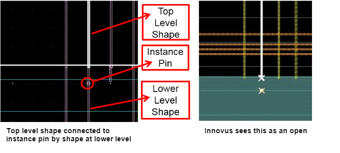
18.2.1.3 Routing shapes for a net should be at the same level
The routing shapes for a net should not be spread across the design hierarchy. If a net is routed in such a manner that the shapes/vias are at different levels, it will be difficult to figure out the levels to assemble in Innovus to expose the entire path at the top. In addition, it might not be possible to create the correct connectivity.
No opens with VXL Extract till level 1
In this design, the routing shapes at level 1 in Virtuoso-XL are fine and no opens are detected when extraction is run for level 1 in Virtuoso. However, Innovus cannot see the lower level shapes, as shown below, and reports opens.
Routing shapes missing in Innovus
18.2.1.4 Object names should match names in sdc file
The names of Layout objects should match with the names in the sdc file. If the sdc file is generated using the schematic as a reference, make sure that the layout and the schematic names also match. The layout should be created using the Generate From Source (GFS), Configure Physical Hierarchy (CPH) and the Generate Physical Hierarchy (GPH) commands. Keep the following points in mind to avoid naming mismatches:
- Avoid using the create instance and copy commands for adding instances because these are not schematic connectivity aware.
- Avoid Many-to-Many instance mappings or manually created instance name mappings because these can cause a mismatch in the names.
- The leading pipe (|) in instance names generated by Virtuoso-XL can cause issues of name mismatch when reading the sdc files. Specify the following variable in the Virtuoso-XL setup to create instances without the leading pipe (|) character:
envSetVal("layoutXL" "prefixLayoutInstNamesWithPipe" 'boolean nil)
18.2.2 Requirements for Correct Connectivity Propagation
For correct connectivity propagation in mixed-signal designs, ensure the following:
18.2.2.1 Logical connectivity
The nets on the instance terminals should be properly connected for logical connectivity to be propagated. Mosaics should be avoided in the design because although Innovus creates the instance from the mosaic, assembleDesign does not map the top-level nets to the lower-level mosaic instances.
18.2.2.2 Pin shape creation
All cells should have shape pins on interconnect layers placed on the cell boundary.
The dot pins used in the design are not understood by Innovus and verifyConnectivity reports opens:
**ERROR: (IMPOAX-641): Found pin shape of type 'Dot' for terminal 'clkin'. Only shapes of type RECT or POLYGON or LINE and vias are supported as pin shapes. This shape will be ignored.
18.2.2.3 Via object creation
OpenAccess via objects should be used and not instances of cells from the library. The create via command should be used to create an OpenAccess via object with a valid viaDef from the technology. Do not use the create instance command or any cell from the library that acts as a via. If you do so, VXL and Innovus would not be able to trace through these instances.
Do not use instances instead of via objects
18.2.2.4 Symbolic type routing
Routing should preferably be of type symbolic. If all the routing is of type geometric, extractRC fails and the following error is reported:
% extractRC: Design must be routed before running extractRC
To prevent such errors, avoid creating paths/rectangles manually. Instead, use the Create -> Wiring -> Wire/Bus or the Auto Routing and point-to-point routing capabilities in Virtuoso to create paths.
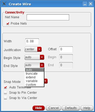
Note that if you choose truncate or extend as begin and end styles, the nets will be read in as regular nets in Innovus. If you choose variable or custom as begin and end styles, the nets will be read in as special nets in Innovus.
18.2.2.5 No MultiPart Paths for bus routing and shielding nets
Avoid the use of MultiPart Paths (MPPs) for bus routing and shielding nets. Use the Create -> Wiring -> Bus feature in Virtuoso for bus routing. Use the Auto Router for shielding the nets. If MPPs are used as buses or to shield nets, make sure that the correct net is set on each of the subpart. Note that MPPs can be used as guard rings because guard rings are not used for timing analysis.
18.2.3 Requirements for OpenAccess Compatibility
For OpenAccess compatibility, the following requirements must be met.
18.2.3.1 Interoperable PDK
A basic requirement for OpenAccess compatibility is an interoperable PDK created by the PDK factory team. To set up an interoperable PDK:
- Import LEF rules into OA database
- Review/compare LEF and OA technology files
- Merge LEF rules with Virtuoso technology data. The additional layer definitions come from LEF import, whereas Virtuoso technology has super set rules.
- Create incremental technology database to include additional data from LEF
For more information on setting up an interoperable PDK, refer to the Technology Data Preparation chapter.
18.2.3.2 OpenAccess Reference Libraries and Cell Setup
For the implementation of a top-level design, OpenAccess libraries must be available for all the standard cells and macros with an abstract view must be available for each cell. If the abstract is not available while reading an OpenAccess design, an abstract is created on the fly from the layout (provided it has the prBoundary object and the pins). The abstract created on the fly contains bare minimum data and allows the flow to continue. However, as such an abstract is not production quality, it should not to be used for production flow.
For the assembleDesign command in Innovus for STA, make sure that the pin count in the layout matches the pin count in the abstracts. In addition, make sure that the pin models are set up properly for the Macros:
- Strongly connected shapes (multiple shapes of one PORT in LEF) indicate that a signal router is allowed to connect to one shape of the PORT, and continue routing from another shape of the same PORT.
- Weakly connected shapes (separate PORTs of the same PIN in LEF) are assumed to be connected through resistive paths inside the MACRO that should not be used by routers. The signal router should connect to one or the other PORT, but not both.
- Mustjoin pins indicate that these are to be connected together by the router outside of the cellview
18.2.3.3 OpenAccess Objects instead of LPPs
OpenAccess interoperability works on database objects and not layer-purpose pairs (LPPs).
- Blockages should be created as an OpenAccess blockage object and not a shape on a layer/purpose pair:
- Use Create -> P&R Objects -> Blockage in Virtuoso to create an OpenAccess blockage object.
- The cell Boundary should be a prBoundary type object and is needed by Innovus for all cells:
- Use Create -> P&R Objects -> P&R Boundary in Virtuoso to create a prBoundary type object. Otherwise, you will get the following error:
**ERROR: (IMPOAX-815): PRBoundary is not present in OA design. Cannot restore the design from given OA database. Correct the data and retry.
- Use Create -> P&R Objects -> P&R Boundary in Virtuoso to create a prBoundary type object. Otherwise, you will get the following error:
- Pins must be created as Pin Objects with shapes on interconnect layers and not as shapes with text on top:
- Use Create -> Pin in Virtuoso and select metal layer as per LDRS to create Pin Objects.
- All metal shapes on any purpose are treated as routing shapes and shorted.
18.2.3.4 Correct sigType for Pins and Nets
Set the correct sigType for the Power and Ground pins and nets. If not, the following warning is generated:
**WARN: (IMPDB-1256): Power pin VDD of instance DFF7 is connected to non-p/g net vdd_1p2v. Mark the net as power net and create associated snet
The top-level power/ground net should be marked global in Virtuoso in case the assembled block has physical-only power/ground pins. Otherwise, the following error is generated:
**ERROR: (IMPOAX-1087): Cannot create instance terminal 'VDD' of instance ‘DFF7' connecting to net ‘vdd_1P2' : A physical-only instTerm cannot connect to a net located in a different occurrence
To set the sigType, select the pins in Virtuoso, and then use the Navigator and the property editor widgets. The proper sigType is needed for marking nets as Analog as well. Nets marked as Analog are ignored by NanoRoute in Innovus.
18.2.3.5 PCell Cache Generation
Generate the parameterized cell (PCell) cache from Virtuoso before loading the OpenAccess DB into Innovus:
- From the Layout in Virtuoso Window, invoke Tools -> Express Pcell Manager.
- Fill in the directory name to save the PCell cache.
- Select the Enable Express Pcells check box.
- Select the Auto Save check box.
- Click Ok.
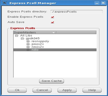
This is equivalent to:
setenv CDS_ENABLE_EXP_PCELL true
setenv CDS_EXP_PCELL_DIR ./.expressPcells
18.2.3.6 Bus Ordering and Continuity
Run Verilog Annotate on the cells to set the bus bit information on the cells' pins before the data is loaded in Innovus. This is needed to set the bus terminal information and order on each cell that has bus pins so that the bus connections can be established properly by Innovus. If this not done, the following warning is generated:
**WARN: (IMPOAX-252): Found BusBit terminals of bus 'i_cnt[1]' of cell ‘Design_Top' without bus ordering information in OA library ‘designLib'. This may lead to problems during saveDesign. It is recommended to run verilogAnnotate on the library for annotating bus ordering information to such terminals.
You also need to make sure that the bus indices are continuous. Otherwise, the following warning is generated:
**WARN: (IMPDB-2080): Non-continuous bus index in cell TESTLV_HIGH_TOP. Missing pin info between A[31] and A[64]
**WARN: (IMPDB-2080): Non-continuous bus index in cell TESTLV_LOW_TOP. Missing pin info between A[63] and A[96]
In addition, the OpenAccess flow at present does not support negative bus indices, such as the following, in the Verilog netlist:
wire [15:-16] CNTRL_O;
wire [15:-16] CNTRL_T;
wire [0:-15] CNTRL_S;
You should use logic synthesis to avoid generating such netlists.
18.2.3.7 Bus Annotation Set by Default
To make sure that the bus annotation is set up by default, enable the option to create implicit inherited terminals while creating the layout in VXL using Generate From Source and Generate Physical Hierarchy (preferred way to design). verilogAnnotate is not needed for blocks created with Virtuoso-XL and abstract Generator post the 615 ISR16 release because this option has been turned on by default from this release. For older cells/IPs, you can export a verilog stub from the symbol view of the cell and run the following command for setting the bus terms and bus order correctly:
verilogAnnotate -verilog block.v –refLibs cellsLib -libDefFile cds.lib -refViews "layout abstract“
18.2.3.8 Fixed or Placed Placement Status
The placement status for instances and pins should be set as placed or fixed.
Sample skill to check/set the status:
% cv~> instances~> status- Returns nil for all instances% cv ~> instances~> status = “placed”- Sets as placed for all instances% cv ~> terminals~> pins~> status- Returns nil for all terminals% cv ~> terminals~> pins~> status = “placed”- Sets placed for all terminals
You can even check or set the status via the property editor.
Innovus has the following option (on by default) to counter this issue:
setOaxMode -instPlacedIfUnknown true - Sets the status for instances from none/unplaced to placed
18.2.4 Useful Utilities and Information
18.2.4.1 Using OpenAccess Mapper for Migration
The OpenAccess Mapper assists to convert the LPP-based shapes to OpenAccess objects and change the layerName for the pins to use the interconnect layers. The OpenAccess Mapper is available at the following path in your installation:
your_Virtuoso_installation/tools/dfII/bin/mapper
The syntax for the mapper is as follows:
mapper -objectmap mapFileName | -map mapFileName -lib libName [-cells cellName] [-views viewName] [-reportallerrors] [-namemap] [-copy]
To move the pins to interconnect layers, use LPP-to-LPP mapping (-map parameter). The sample layer map file syntax is as follows:
MET1PN drawing MET1 drawing
To migrate the boundary/blockage LPP shapes to OpenAccess objects, use object mapping (-objectmap parameter). The sample object map file syntax is as follows:
BOUNDARY drawing boundary pr
MET1 obs blockage route
MET1 dbk blockage fill
For more information about the OpenAccess Mapper utility, refer to the chapter "Post-Processing of the Translated Data" of the cdboa.pdf document at
your_Virtuoso_installation/doc/cdboa/cdboa.pdf.
18.2.4.2 Using GDS flow for Setting Up Layer/Object Map Files
The following are samples of the Virtuoso stream out layer and object map files which can be useful in the OpenAccess flow:
- Layer mapping for pin shapes: Assume there are pin shapes and some regular shapes on the same LPP (M4 drawing):
- If the layer map is "
M4 drawing 8 1":
All shapes onM4 drawingdata will go on the stream layer purpose <8:1>. - If the layer map is "
M4 drawing 7 1 pin":
All pin shapes onM4 drawingwill go on the stream layer purpose <7:1>.
- If the layer map is "
- Object mapping for blockages or boundary: A sample object map file for stream out is as follows:
Boundary PR 1 1layerBlockage routing MET1 2 2 (for “MET obs” lpp)layerBlockage fill MET1 3 3 (for “MET dbk” lpp)
For more information, refer to the Virtuoso streamOut document available at $CDSHOME/ doc/transrefOA/transrefOA.pdf.
18.2.4.3 Using OpenAccess Database Checker for Verification
The OpenAccess Database Checker (OA DB Checker) allows you make various checks for the technology and design setup to achieve OpenAccess interoperability between Virtuoso and Innovus. Broadly, the OA DB Checker allows you to check for the following:
- Technology setup, such as constraint groups and so on
- Design objects and OpenAccess compliance, such as prBoundary
- Setup required for interoperability like PCell cache and bus annotation
- Design constraints
For more information about this utility, refer to the OpenAccess Database Interoperability Checker chapter.
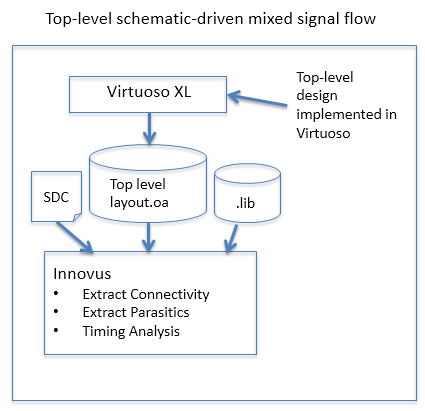
In the above example, the top-level design is implemented in Virtuoso using a schematic for top level. It can be brought over to Innovus through the OpenAccess database to run timing analysis between digital logic of AMS block and digital P&R block.
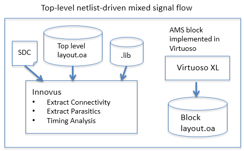
The above example shows the case where the top level is implemented in Innovus through a Verilog netlist. After the physical layout is implemented, it is possible to perform timing analysis on the timing paths between the digital logic at the top physical level and the digital logic at the lower physical level of the AMS block.
18.3 Handling Schematic-Driven Designs Implemented Using a Non-Interoperable PDK
As mentioned earlier in the Requirements for OpenAccess Compatibility section, an Interoperable PDK is required to provide an interoperable technology library for the design. For schematic-driven designs, it is possible that the designs were already implemented based on a non-interoperable (or a non-MSOA) PDK long before the interoperable PDK was available. This section discusses what can be done to run static timing analysis in such a situation without making significant changes. Note that the interoperable PDK is still needed but some steps are needed to re-reference the top-level design, or a copy of the top-level design, to the interoperable PDK.
18.3.1 Checking the Technology Database Graph of a Specific Design Library
To check the technology library to which the design is referenced or attached, you can run either Virtuoso or Innovus:
18.3.1.1 Checking in Virtuoso
For Virtuoso, use the Technology Tool Box that can be invoked from the Command Interface Window (CIW). To check the technology library of a specific design library, perform the following steps:
-
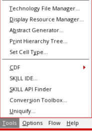
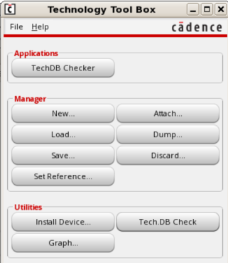
In the CIW, select Tools -> Technology File Manager to invoke the Technology Tool Box.
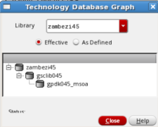
- In the Technology Tool Box, click the Graph button to invoke the Technology Database Graph form.
- In the Technology Database Graph form, click the Library drop-down list to select the design library to be verified.
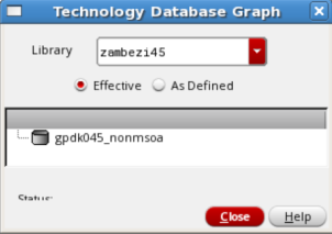
In this example,zambezi45is selected. The Technology Database graph form shows that the design library,zambezi45is attached to thegpdk045_nonmsoatechnology library. Note that thegpdk045_nonmsoatechnology library is not interoperable (that is,it is non-MSOA).
18.3.1.2 Checking in Innovus
Alternatively, you can determine the tehcnology library in Innovus by using the report_oa_lib command with the -filter tech_graph option.
For the same example as above, the command will be"
> report_oa_lib zambezi45 -filter tech_graph
Innouvs will report the following in the log file:
Technology Graph:
Zambezi45
gpdk045_nonmsoa (attached)
18.3.2 Opening a Design Attached to a Non-Interoperable PDK in Innovus
When a non-interoperable PDK-based design is loaded in Innovus, the tool may issue some error messages.
For example, assume that the top-level design is the layout view of cell LP_pll from the zambezi45 library, and a script containing the following commands is run to load the design cellview into Innovus:
Here, assume that set init_design_netlisttype {OA}set init_oa_design_lib {zambezi45}set init_oa_design_cell {LP_pll}set init_oa_design_view {layout}set init_oa_ref_lib {gsclib045}set init_mmmc_file {scripts/LP_pll.viewDefinition.tcl}init_designgsclib045 is the MSOA technology library that is based on an interoperable PDK ITDB. Now, although gsclib045 is specified with init_oa_ref_lib, but as the zambezi45 design is based on gpdk045_nonmsoa library, Innovus will still read the technology information from gpdk045_nonmsoa.
Innovus may issue error messages, such as the following:
Reading tech data from OA library 'zambezi45' ...
...
**ERROR: (IMPOAX-1304): Base constraint group name 'LEFDefaultRouteSpec' for reading all the rules is not found. Provide one or change the base constraint group using 'set init_oa_default_rule <name>' and read the OA database again.
**ERROR: (IMPSYT-6692): Invalid return code while executing 'run.tcl' was returned and script processing was stopped. Review the following error in 'f1.tcl' then restart.
**ERROR: (IMPSYT-6693): Error message: run.tcl: **ERROR: (IMPSYT-16006): Fail to read LEF information from OA reference libraries. Check the OA database provided and your inputs.
18.3.3 Ways To Switch a Design Library from a Non-Interoperable to an Interoperable PDK
The loading of the design requires the technology library to be based on an interoperable PDK. You can resolve the above issue, without having to re-implement the design, by following either of the two approaches described below:
18.3.3.1 Re-Referencing the Design Library to an Interoperable PDK
Assume that the interoperable PDK is an ITDB with the following hierarchy:
gsclib045 (second level) => gpdk045_msoa (base level)
If the original design is attached to a non-MSOA PDK, the update_oa_lib command in Innovus can be used to switch the kind of relationship from “Attach” to “Reference”:
For example, to switch the zambezi45 design library to reference to the gsclib045 library, perform the following steps:
-
Run the following command in Innovus:
update_oa_lib -tech_attach_to_reference zambezi45
Upon completion, Innovus issues a message similar to the following:Successfully converted the library 'zambezi45' to use a tech reference from the attached tech. -
In Virtuoso, in the CIW, select Tools -> Technology File Manager to invoke the Technology Tool Box.
-
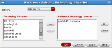
In the Technology Tool Box, click the Set Reference button to open the Referencing Existing Technology Libraries form.
- From the Library drop-down list in the Referencing Existing Technology Libraries form, select the zambezi45 library:
-
Select
gpdk045_nonmsoain the Reference Technology Libraries list and click the <- button so that it is no longer the reference library. Then, selectgsclib045in the Technology Libraries list and click the -> button so that it appears under the Reference Technology Libraries list as shown below: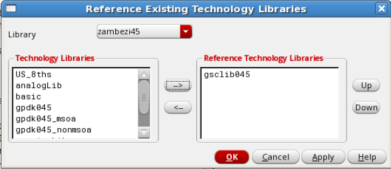
- Click the OK button to commit the changes.
-
Now, verify the technology graph of the design library by performing the steps described in the Checking the Technology Database Graph of a Specific Design Library section.
Note that thezambezi45design library now references thegsclib045library.
18.3.3.2 Copying the Top-Level Cellview to a New, Interoperable PDK-Based Design Library
The second approach is to create a new design library that is based on the interoperable PDK and copy the top-level cellview to this new design library. Note that only the top-level cellview is to be copied; copying of the cellviews of lower levels are not required. Then, load the top-level cell view from the new design library into Innovus for timing analysis:
- In the Library Manager, select File -> New -> Library to open the New Library form. Then, specify a new design library name, such as
zambezi45_msoaand click the OK button.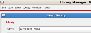
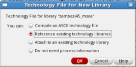
- In the Technology File for New Library form, select the Reference existing technology libraries option and click the OK button.
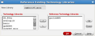
- In the Reference Existing Technology Librariesform, scroll to the desired MSOA library (for e.g.
gsclib045), select it and click the -> button to move it to the Reference Technology Libraries list.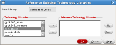
- Click the OK button to commit the change.
- In the Library Manager, select the top-level cellview of the original design library and choose Copy.
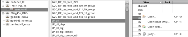
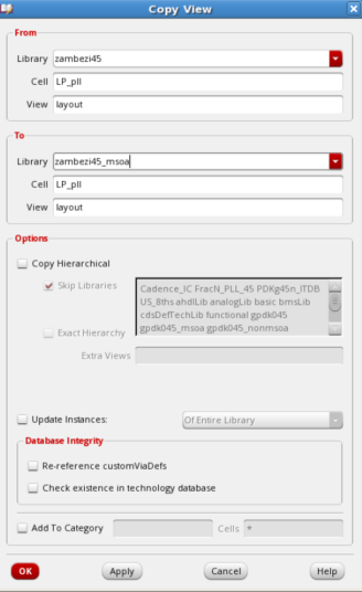
-
In the Copy View form, select Zambezi45_msoa from the Library drop-down list in the To section. Keep the Cell and View names in the To section the same as that in the From section. Click OK to commit the copy.
-
Load this cellview
zambezi45_msoa LP_pll layoutinto Innovus to run the static timing analysis flow:set init_design_netlisttype {OA}set init_oa_design_lib {zambezi45_msoa}set init_oa_design_cell {LP_pll}set init_oa_design_view {layout}set init_oa_ref_lib {gsclib045}set init_mmmc_file {scripts/LP_pll.viewDefinition.tcl}init_design
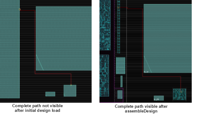
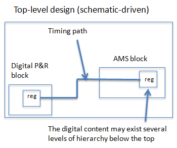
18.4 Running STA by Flattening the Design
In this method, the Innovus command assembleDesign is used to flatten the physical hierarchy to bring the instances and wires at the lower physical level to the top for parasitic extraction and timing analysis.
Note that the physical hierarchy of the design is flattened only to enable static timing analysis. It does not alter the physical structure of the design in any way.
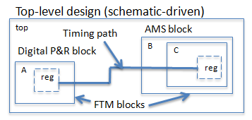
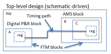
To time a path between registers inside a digital P&R block and an AMS block, the following shows the flow diagram of running STA using the flatten approach on a top-level, schematic-driven design.
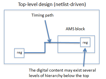
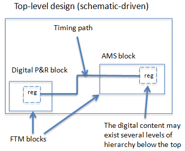
For a netlist-driven, top-level design, the following shows the flow diagram of running STA on the timing paths between the register at the top and the register inside the AMS block using the flatten approach.
18.4.1 Steps for Running STA Using the Flatten Approach
You can run STA on your design using the following steps:
- Load the top-level design
- Flatten the blocks
- Load and commit power intent, if necessary
- Specify Parasitic Extraction options
- Run static timing analysis
18.4.1.1 Load the top-level design
If the top-level design is originally a schematic-driven design implemented by Virtuoso, the init_design command should be used to load the OpenAccess design:
For a top-level design that is netlist-driven, If the design is saved by Innovus into a cellview, Note: Innovus uses the following order of precedence to determine which technology library to use: Therefore, when using an OpenAccess cellview as the design, the tech lib always comes from the design library that contains the cellview. In this case, the set init_design_netlisttype {OA} set init_oa_design_lib {mylib} set init_oa_design_cell {top} set init_oa_design_view {layout} set init_oa_ref_lib {gsclib045} set init_pwr_net {VDD AVDD} set init_gnd_net {GND AGND} set init_mmmc_file {viewDefinition.tcl} init_designinit_design can be used to start the place and route flow. The following example shows how to specify the init global variables.set init_design_netlisttype {Verilog} set init_verilog {top.v} set init_oa_ref_lib {gsclib045} set init_pwr_net {VDD AVDD} set init_gnd_net {GND AGND} set init_mmmc_file {viewDefinition.tcl} init_designrestoreDesign can be used to retrieve the OpenAccess database.lib from restoreDesign -cellview "lib cell view"init_oa_design_libinit_oa_ref_lib listinit_oa_ref_lib list is used only for loading cells and not for technology information. The first lib in the init_oa_ref_lib list is used for technology information only when the design is read from a Verilog netlist.
18.4.1.2 Flatten the blocks
For the top-level, schematic-driven design shown below, the two blocks can be flattened by running the following commands:
assembleDesign -block {mylib B layout} -block {mylib C layout}
assembleDesign -block {mylib D layout}
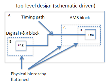
Similarly, to flatten an AMS block that has digital logic one level below the top, the following Tcl command can be run:
assembleDesign -block {mylib B layout}
Note: In the above example, assembleDesign is run in the incremental mode. You can also run assembleDesign in the batch mode. Refer to the section "Different Ways of Running assembleDesign" for details.
18.4.1.3 Load and commit power intent if necessary
This step is required only when the digital logic to be timed belongs to more than one power domain. In such a situation, you have to load and commit the Common Power Format (CPF) file because the CPF file provides information about the instance's power domain. It is possible that two instances placed in different power domains are of the same cell type (same physical design). However, when the instances are placed in different power domains with connections to different power signals (for example, one is dvdd and the other is VDDsw), a CPF file is necessary to let Innovus know which timing library set should be used for these two instances.
An example of the Tcl script for this step is:
read_power_intent -cpf top_design_flat.cpf
 commit_power_intent -keepRows
The main purpose of specifying -keepRows is to instruct Innovus to keep the rows of the digital P&R block (if present). It is recommended to use this option for commit_power_intent in hierarchical flow (after assembleDesign is used). If the -keepRows option is not specified, commit_power_intent removes the existing rows by default and recreates them. If the rows of the assembled block are not aligned with the rows at the top, the newly created rows will be misaligned with the instances that are brought to the top from the P&R block.
18.4.1.4 Specify parasitic extraction options
Typically, when the design is already routed, the extraction engine should be set to the postRoute mode to enable detailed extraction of the wires and to report coupling.
setExtractRCMode -engine postRoute
For accuracy, you can use the correct extraction engine setting to use standalone Quantus or Integrated Quantus (IQuantus) from Innovus. To invoke the IQuantus extraction engine,
setExtractRCMode -effortLevel high
To invoke the standalone Quantus extraction engine, use the signoff option and provide a layer-mapping file between the Quantus technology file and the technology library used in Innovus.
setExtractRCMode -effortLevel signoff
setExtractRCMode -lefTechFileMap Quantus_LEF.layermap_10lm.oxide
18.4.1.5 Run timing analysis
To run timing analysis, use:
report_timing
or
timeDesign -postRoute
The above commands will automatically run parasitic extraction before analyzing the timing path, if the tool has not performed parasitic extraction earlier.
18.5 Running STA by Using the FTM
The process of running STA by using the FTM can be divided into two main tasks:
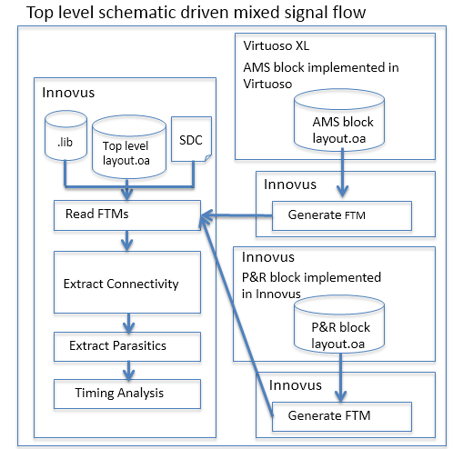
The following shows the flow diagram of running STA using the FTM approach on a top-level schematic-driven design.
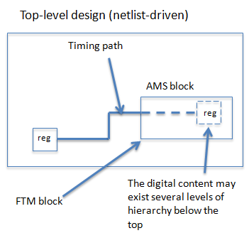
The following diagram depicts the flow for running STA using the FTM approach on a top-level netlist-driven design.
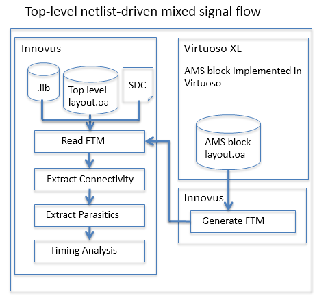
18.5.1 Generating the FTM for Each Block
You can generate the FTM for your blocks using the following steps:
- Load the block design.
- Flatten sub-blocks, if necessary.
- Load and commit power intent, if necessary.
- Specify the parasitic extraction options.
- Create and save the FTM.
18.5.1.1 Load the block design
If the block design is implemented using Innovus, restoreDesign can be used to load the design. If the block design is originally a schematic-driven design implemented by Virtuoso, the init_design command should be used to load the OpenAccess design. For example, to create the FTM block for block B below, run init_design with the following:
set init_design_netlisttype {OA}set init_oa_design_lib {mylib}set init_oa_design_cell {B}set init_oa_design_view {layout}set init_oa_ref_lib {gsclib045}set init_pwr_net {VDD AVDD}set init_gnd_net {GND AGND}set init_mmmc_file {viewDefinition.tcl}init_design
18.5.1.2 Flatten sub-blocks if necessary
For the example shown above, because the logic instances to be timed are at a lower level (in the sub-block C), it is necessary to flatten the sub-block using assembleDesign.
assembleDesign -block {mylib C layout}
18.5.1.3 Load and commit power intent if necessary
If the block is a low power design, load and commit the CPF file. For example:
read_power_intent -cpf block_flat.cpf
commit_power_intent -keepRows
18.5.1.4 Specify the parasitic extraction options
Typically, when the design is already routed, the extraction engine should be set to the postRoute mode to enable detailed extraction of the wires and report coupling.
setExtractRCMode -engine postRoute
For accuracy, you can use the correct extraction engine setting to use standalone Quantus or IQuantus from Innovus.
To invoke the IQuantus extraction engine, use the following command:
setExtractRCMode -effortLevel high
18.5.1.5 Create and save the FTM
To create the FTM, use the createInterface-removePowerGroundLogic command with the -keepAll option to keep the full Verilog netlist. This will ensure that there is no trimming of any logic. This command will run RC extraction and save the RC parasitic information and netlist along with the cell view location specified by the -cellview option.
createInterface-removePowerGroundLogic -cellview {mylib B layout} -keepAll
If a design is originally created in Virtuoso, it is common to see power/ground ports and nets created in the netlist database of the FTM model. Tools like Genus do not accept the FTM model with power/ground ports or net. To create an FTM that has no power/ground ports and nets, specify the -removePowerGround option.
createInterface-removePowerGroundLogic -cellview {mylib B layout} -keepAll -removePowerGround
Note: The saved FTM data will be used in top-level analysis and the library, cell, and view name will be used to help the tool determine the location of the FTM data.
18.5.2 Running STA on Top-level Design with FTM of Blocks
You can run STA on your design with the FTM of blocks using the following steps:
- Load the top-level design
- Specify FTM blocks
- Switch to the ILM view
- Load and commit power intent, if necessary
- Specify parasitic extraction options
- Run timing analysis
18.5.2.1 Load the top-level design
If the top-level design is originally a schematic-driven design implemented by Virtuoso, the init_design command should be used to load the OpenAccess design:
For a top-level design that is netlist-driven, If the design is saved by Innovus into a cellview, set init_design_netlisttype {OA}set init_oa_design_lib {mylib}set init_oa_design_cell {top}set init_oa_design_view {layout}set init_oa_ref_lib {gsclib045}set init_pwr_net {VDD AVDD}set init_gnd_net {GND AGND}set init_mmmc_file {viewDefinition.tcl}init_designinit_design can be used to start the place and route flow. The following example shows how to specify the global init variables.set init_design_netlisttype {verilog}set init_design_netlisttype {top.v}set init_oa_ref_lib {gsclib045}set init_pwr_net {VDD AVDD}set init_gnd_net {GND AGND}set init_mmmc_file {viewDefinition.tcl}init_designrestoreDesign can be used to retrieve the OpenAccess database.
Notes:
- The timing constraint file(s) used for FTM analysis should be a "flat" type constraint file that contains the constraints for the top design and instances inside the block. The top-design-only timing constraint file that constrains till to the boundary of the block should not be used for FTM analysis.
- For timing analysis done with FTM blocks, the timing constraint file must be specified using the
-ilm_sdc_filesoption, whether it is for thecreate_constraint_modestatement inviewDefinition.tcl,or for theupdate_constraint_mode,which is an interactive command.
For example, in the viewDefinition.tcl loaded into the top-level global file, the timing constraint file to be used for FTM analysis, top_flat.sdc is specified as follows:
create_constraint_mode -name mode1\
-sdc_files [list ../DATA/top.sdc] -ilm_sdc_files {../DATA/top_flat.sdc}
If the -ilm_sdc_files option of create_constraint_mode in the viewDefinition.tcl is not specified, you can run update_constraint_mode after init_design as follows:
update_constraint_mode -name mode1 -ilm_sdc_files {../DATA/top_flat.sdc}
18.5.2.2 Specify FTM blocks
This step is to specify the FTM location for each block to be read as FTM.
specifyIlm -cellview {myLib A layout}
specifyIlm -cellview {myLib B layout}
By using the -cellview option of specifyIlm, the tool is able to find the OpenAccess path based on the cds.lib in the current working directory.
Note: If the FTM approach is used for the above example, only one assembleDesign is done to flatten sub-block C when generating the FTM for block B. In the flat approach, after the top-level design is loaded into Innovus, block A and block B have to be flattened using assembleDesign, while in the FTM approach, they are only specified as FTM blocks (no flattening is done.)
18.5.2.3 Switch to the ILM view
Switch to the ILM view by running the following command:
flattenIlm
While this command is being run, Innovus reads in the logical netlist and parasitic information of each FTM block. After the command completes running, the tool issues the following statement:
*** Switch to ILM view done
In the default mode (blackbox view), all FTMs blocks are perceived as blackboxes. The tool sees the connectivity only down to the boundary level (ports) of FTM. Switching to the ILM view enables the tool to see the instances and nets inside the FTM block(s). The physical boundary of the FTM block will be transparent to the tool in this ILM view. The tool now has the logical connectivity information for the instances inside the FTM block(s) to run timing analysis. For example, it is able to report timing on a path that starts from an instance outside the FTM block and ends at an instance inside the FTM block.
Note: Some commands that perform physical-only functions, such as verifyConnectivity, are not supported in this mode. Therefore, some of the top menus, such as Floorplan and Verify, appear grayed out in the main window in this mode. To run these commands, return to the default mode (blackbox view) by specifying the following command:
unflattenIlm
18.5.2.4 Load and commit power intent if necessary
Similar to the step done in flatten approach (see Steps to Run Static Timing Analysis using the flatten approach), this step is only required when the digital logic to be timed belongs to more than one power domain. An example of the TCL script for this step is as follows:
read_power_intent -cpf top_design_flat.cpf
commit_power_intent -keepRows
Note: The above two commands have to be specified after flattenIlm. The CPF file specified has to be a flat CPF (i.e. not a hierarchical CPF) that contains detailed specification for instances inside the FTM block(s). The macro model, which contains power domain information at the boundary port level, is not detailed enough for the FTM block(s). It is okay to use the macro model to represent non-FTM blocks.
18.5.2.5 Specify parasitic extraction options
Typically, when the design is already routed, the extraction engine should be set to postRoute mode to enable the detailed extraction of the wires and to report coupling.
setExtractRCMode -engine postRoute
To invoke the IQuantus extraction engine, use the following command:
setExtractRCMode -effortLevel high
18.5.2.6 Run timing analysis
To generate full and detailed timing reports, specify:
timeDesign -postRoute
The above command automatically runs parasitic extraction before analyzing the timing path if the tool has not performed parasitic extraction earlier.
Alternatively, you can run the following command to report information about the various paths in the design:
report_timing
Note: The report_timing command must be specified after flattenIlm.
Note: Make sure the timing constraint file is specified using -ilm_sdc_files (Refer to Note in "Load the top-level design" step.)
If the timing constraint files for FTM analysis are not specified using either create_constraint_mode –ilm_sdc_files or update_constraint_mode –ilm_sdc_files, Innovus issues the following message:
No constrained timing paths found.
Paths may be unconstrained (try '-unconstrained' option)
18.6 Difference between Flat and FTM Approaches
The following table compares the FTM and flat approaches.
| FTM | Flat | |
|---|---|---|
| Dealing with Physical hierarchy |
No |
Runs one or more assembleDesign till instances are seen on top level |
|
Representation of the block |
The block is represented by a Verilog netlist and SPEF file(s) for the RC parasitic which make it portable. | Does not require writing out the logical connectivity in the Verilog netlist and RC parasitic in the form of SPEF for the block. Innovus extracts the logical connectivity and RC parasitic from the flattened block. |
|
Usability and Debugging |
|
|
18.7 Guidelines for Running STA Flow on Mixed-Signal Design
Consider the following guidelines before running the design data flow:
- The mixed-signal block physical implementation must be done using the VLS-XL connectivity-driven physical implementation methodology using Configure Physical Hierarchy (CPH) and Generate Physical Hierarchy (GPH) methodology. Multiple logical hierarchies in the design netlist are fully supported.
- While in the Virtuoso platform, do not copy a library or cell or view and save it by changing the cell name. This will cause problems while reading the changed cell name view in Innovus.
- The physical database created in Innovus after running assembleDesign on AMS block should not be used for any physical implementation steps or while exporting GDS. The physical database is only for analysis.
- Names of objects (for example, instances) in timing constraint must match the layout design loaded into Innovus. This implies that:
- If the instance in the layout has a pipeline character (i.e. "|"), the corresponding statement in the timing constraint that has constraint over this instance must contain the pipeline character as well.
- The hierarchy of the instances must match between the layout and timing constraint.
18.8 Creating a Quick Timing Model for Analog IPs in Innovus
In the netlist-on-top flow, the design could contain one or more analog blocks/IPs. The what-if timing analysis capability in Innovus allows for the creation of a quick timing model for such blocks, so that timing analysis can be performed at the top level. For more information on what-if timing model creation capability, refer to the "What-If Timing Analysis" chapter of the Innovus User Guide.
For the what-if timing model creation to work in Innovus, you need to set the blocks as blockBlackBox while using Virtuoso.
Following is the description of how a block is converted to a black box in Virtuoso.
- Set the cellType to blockBlackBox.
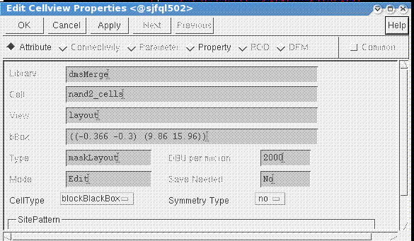
- Now when you run
restoreDesign -cellview, you see the cloned instances as black boxes. This was done with a quick abstract, but can also be done with an abstract cellview.
- The black box can now be modified for What-If Timing analysis.
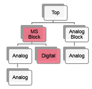
18.9 Different Ways of Running assembleDesign
The assembleDesign command supports different types of data. It can read an FE database, such as a DEF file and a Verilog netlist file, as well as an OpenAccess (OA) database. For the mixed-signal flow, the OA-based database should be used for interoperability. You can use the -topDesign and -block options of assembleDesign to specify the library, cell, and view information for the top-level design and the blocks, respectively. Options such as -topDir, -blockData and -blockDir are meant for non-OA type data and will not be discussed here.
You can run the assembleDesign command in two modes, batch and incremental. It is also possible to start an Innovus session by running assembleDesign in the batch mode followed by running incremental assembleDesign for blocks that are at the next lower hierarchy.
When running in the incremental mode, you can also use the -allTimingBlocks option, without the need to specify the library, cell and view information, which allows the tool to perform automatic detection and assembly of blocks that has digital content. The -allTimingBlocks option can be used with the -blockCell option to force certain blocks to be assembled manually, the -exceptBlocks option to override the default list and exclude certain blocks from being assembled, or both.
18.9.1 Running assembleDesign in the Batch Mode
When running assembleDesign in the batch mode, a new Innovus session is initiated. After loading the top-level design and block(s), assembleDesign performs physical flattening and assembles the top-level design and block(s) together. In this mode, the library, cell, and view names of the top-level design and the block(s) are specified together. The following command shows how to run assembleDesign in batch mode to flatten two blocks, blockA and blockB, which are one physical level below the top-level design, top:
assembleDesign -topDesign myLib top layout_for_asm -block {myLib blockA layout} -block {myLib blockB layout} -mmmcFile flat.viewDefinition.tcl
18.9.1.1 Loading a Design that Is Not Saved in Innovus
To run assembleDesign in batch mode, the top-level design must be such that it can be restored in Innovus.
For Innovus to read or restore an OA-based database, it requires the presence of a Here is a sample script to load the top-level design and migrate it to an Innovus-restorable design:.global file, which contains the specification of various variables. The variables that have init as prefix are used by Innovus to initialize the design. If the top-level design has not been saved in Innovus, for example, if it is implemented through Virtuoso, use the init_design command to load it, and then use the saveDesign command to migrate it to an Innovus-restorable design. After saving it into a new design, the new database will contain the .global file with no change to the original physical layout database.set init_design_netlisttype {OA}set init_oa_design_lib {mylib}set init_oa_design_cell {top}set init_oa_design_view {layout}set init_oa_ref_lib {gsclib045}init_designsaveDesign -cellview {myLib top layout_for_asm}exit
Alternatively, you can do the above through an interactive session using GUI as follows:
- Invoke Innovus to start a new session.
- From Innovus menu bar, select File > Import Design.
- Fill in the variables and click OK when done.
- After the design is loaded, select File > Save Design from the menu bar.
- Specify the library name and a new view name. Click OK when done.
- Exit Innovus.
18.9.1.2 MMMC Configuration File and Terminology
To run STA, Innovus requires the Multi-Mode Multi-Corner (MMMC) settings to be specified. This configuration file is typically named as viewDefinition.tcl. In this file, timing-related information, such as timing libraries, PVT (process, variation and temperature) operating conditions for the cells in the design, and the timing constraint file are specified. The MMMC configuration file also contains the information needed to run parasitic extraction for wire resistance and capacitance, such as technology file details.
Note: Though named MMMC, the configuration file supports single mode and single corner as well. The single mode and single corner settings are similar but simpler as compared to MMMC settings.
The term top-level timing constraint file is ambiguous in hierarchical flow and STA flow for mixed-signal design. To avoid confusion:
- The timing constraint file that contains constraints for only the top-level module (without covering the blocks) is called the top-level only timing constraint file
- The timing constraint file that contains constraints for the full chip (top module + block) is called the flat, full chip timing constraint file. To run STA in a flattened design or when FTM is used, the flat, full chip timing constraint file should be used.
18.9.1.3 Loading the MMMC Configuration File in the Batch Mode
In the batch mode, use the -mmmcFile option of assembleDesign to load an MMMC configuration file that contains the flat, full chip timing constraint and settings for the flattened design. The MMMC configuration file that might be available in the top-level design will be ignored by assembleDesign after the assembly.
Alternatively, the -cpfFile option of assembleDesign can be used instead of -mmmcFile if the CPF file has the MMMC settings.
Note: The -cpfFile option instructs assembleDesign to load the timing-related settings specified in the CPF file to initialize the MMMC settings for running STA. It does not load all the power intent related specification contained in the CPF file. After assembleDesign, the read_power_intent -cpf and commit_power_intent commands are still needed to be loaded to commit all the power intent specification contained in the CPF file.
18.9.2 Running assembleDesign in the Incremental Mode
To run assembleDesign in incremental mode, the top-level design must be already loaded. In the example shown below, the top-level design is not saved in Innovus. The init_design command initializes and loads the design with the init variables provided. After the top-level design is loaded, the specified block is then flattened using the assembleDesign command. An example is shown below:
set init_oa_design_lib {myLib} set init_oa_design_cell {top} set init_oa_design_view {layout} set init_design_netlisttype {OA} set init_mmmc_file {top.viewDefinition.tcl}
init_design assembleDesign -block {myLib blockA layout} -block {myLib blockB layout}
If the top-level design is previously saved in Innovus, the restoreDesign command can be used to load the design. Then, run assembleDesign with the specified blocks to perform incremental assembly.
restoreDesign -cellview {mylib top layout}
assembleDesign -block {myLib blockA layout} -block {myLib blockB layout}
The incremental mode allows the assembleDesign command to be run multiple times in sequence to flatten blocks of multiple levels of physical hierarchy (for example, blocks within blocks). For example, assume there are two blocks, blockA and blockB, in the top-level design to be flattened. blockA has a sub-block, blockAa, while blockB has blockBb as its sub-block. Both blockAa and blockBb are to be flattened.
The following script can be used to assemble them incrementally. Each assembleDesign command flattens the design for one level of physical hierarchy.
assembleDesign -block {myLib blockA layout} -block {myLib blockB layout}
assembleDesign -block {myLib blockAa layout} -block {myLib blockBb layout}
Thus, the incremental capability of assembleDesign enables the physical flattening of a design with multiple levels of physical hierarchy through a single Innovus session.
18.9.2.1 Loading the MMMC Configuration File in the Incremental Mode
The top-level design must be loaded before assembleDesign is run in incremental mode. In addition, the top-level design must contain an MMMC configuration file. If not, Innovus will go into the physical-only mode. Typically, this MMMC configuration file contains the top-level only timing constraints. To reload a new flat, full chip timing constraint file, you must source it after assembleDesign as follows:
You can specify an MMMC configuration file that has the flat, full chip timing constraint file when the design is loaded using set init_oa_design_lib {myLib} set init_oa_design_cell {top} set init_oa_design_view {layout} set init_design_netlisttype {OA}
set init_mmmc_file {top.viewDefinition.tcl}
init_designassembleDesign -block {myLib blockA layout} -block {myLib blockA layout} source flat.viewDefinition.tcl init_design as follows. set init_mmmc_file {flat.viewDefinition.tcl}
In this case, you need not reload the MMMC configuration file after assembleDesign. The only drawback for this flow is that Innovus may issue warning and error messages while reading the MMMC configuration file during init_design. When the flat, full chip timing constraint file contains constraint statements on objects, such as instances, or paths that are inside the blocks to be assembled, Innovus issues messages that the specified path or objects could not be found. This is because those paths or objects will exist only after assembleDesign. Therefore, at this point in time, certain constraint statements in the timing constraint will be deemed to be invalid before assembleDesign.
Notes
- The
-mmmcFileoption of theassembleDesigncommand is meant only for batch mode. - The incremental capability of the
assembleDesigncommand does not currently support a design that has a physical netlist. For example, the netlist hasVDDandVSSas input ports in the module. Run the commandsaveNetlist design.vto check whether the netlist has power and ground ports. Run batch modeassembleDesignto handle this type of design. One way of running batch modeassembleDesignto handle such a design with multiple levels of physical hierarchy can be as follows:
#First Innovus session
assembleDesign -topDesign {myLib top layout_for_asm} -block {myLib blockA layout} -block {myLib blockB layout}
saveDesign -cellview {myLib top layout_stage1}
exit
#Second Innovus session
assembleDesign -topDesign {myLib top layout_stage1} -block {myLib blockAa layout} -block {myLib blockBb layout} -mmmcFile flat.viewDefinition.tcl
18.9.3 Differences between the Batch and Incremental Modes of assembleDesign
| Batch Mode | Incremental Mode | |
|---|---|---|
| Loading the top-level design | The top-level design and block(s) are loaded using -topDesign and -block, respectively. The -topDesign option is used only in the batch mode. |
The top-level design must be loaded first using init_design or restoreDesign. The top-level design is never specified using assembleDesign. |
|
Use of command/ |
Use only once. The top-level design and the block(s) must be specified together. |
Can be used multiple times to specify different blocks or blocks at different levels of physical hierarchy. |
| Need to save the top-level design in Innovus | The top-level design must be saved by Innovus before. (assembleDesign uses similar function as restoreDesign to load the top-level design). For a design from Virtuoso, use init_design to load and save the design with a new view name. Then specify the new view name using the -topDesign option of assembleDesign. |
The top-level design does not need to be saved by Innovus before. This means you can use init_design to load a design implemented using Virtuoso. |
Loading viewDefinition.tcl |
Use the -mmmcFile or the -cpfFile option of assembleDesign to load viewDefinition.tcl. These two options are meant for the batch mode only. |
viewDefinition.tcl is loaded with init_design or restoreDesign. |
18.9.4 Running assembleDesign with the -allTimingBlocks Option
When the -allTimingBlocks option is specified, the assembleDesign command uses the following criterion to determine if a cell is to be assembled:
- A standard cell (with CORE celltype) exists in the cellview.
- The cellview has a cell that is bound with the timing library, thus requiring the
viewDefinition.tcland the timing library files to be loaded in the beginning of the flow. - Any of the cellview below the current level of the cell has met either of the above two conditions.
Note: If a cellview itself is bound with timing library, it will not get flattened.
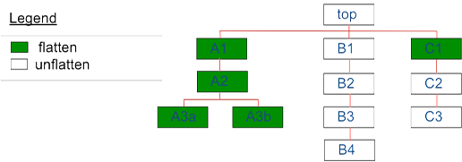
For example, consider a design that has the physical hierarchy shown above. The cellviews at its lower hierarchy bear the following conditions:
- A3a has a standard cell.
- A3b has a cell bound with the timing library.
- None of the B* cells have standard cells or cells bound with the timing library.
- C2 itself is bound with the timing library.
The cellview will be assembled as follows due to the reasons stated below:
- A3a will be flattened because there is standard cell in it.
- A2 and A1 (the cellviews above A3a) will be flattened because A3a has to be flattened.
- A3b will be flattened because there is cell in this cellview bound with the timing library.
- A2 and A1 (the cellviews above A3b) will be flattened because A3b has to be flattened.
Note: As long as either A3a or A3b is to be flattened, the A2 and A1 cellviews will be flattened as well. - None of the B* cells are flattened because no digital content is found at any level.
- C1 will be flattened because C2 (i.e. a cell in C1) is bound to the timing library
- C2 and C3 will not be flattened because C2 has to be a leaf cell, which has timing library bound.
18.9.5 Tips on Running assembleDesign -allTimingBlocks
- View the log file to see which blocks are flattened.
One example is shown below:<CMD> assembleDesign -allTimingBlocks -exceptBlocks {pll_lf pll_lpf pll_vcodiv pll_cp pll_pfd} -blockCell {LP_pll_dig_wSPI}This command "assembleDesign -allTimingBlocks -exceptBlocks {pll_lpf ..." required an extra checkout of license invs_ms.Additional license(s) checked out: 1 'Innovus_MS_Opt' license(s)Following 4 blocks (lib cell view) would be assembled:block 1: zambezi45 LP_pll_dig_combo layoutblock 2: zambezi45 LP_pll_dig_wSPI layoutblock 3: zambezi45 pll_fbdiv layoutblock 4: zambezi45 pll_ls_dvdd2avdd layout -
View the verbose log file to see the reason why a block is flattened or not flattened.
Some sample statements are shown below.
[07/09 14:38:44 13s] Block zambezi45/pll_lf/layout would NOT be assembled as it is excluded by user.[07/09 14:38:44 13s] Block zambezi45/pll_bypclf/layout would NOT be assembled as it does not have any instance of leaf cell or timing library cell inside.[07/09 14:38:44 13s] Block zambezi45/pll_pfd/layout would be assembled as it has instance of standard cell.[07/09 14:38:44 13s] Block zambezi45/LP_vco/layout would be assembled as it has sub block (zambezi45/pll_vco_calsw/layout) which is detected to be assembled.[07/09 14:38:44 13s] Block zambezi45/pll_ls_dvdd2avdd/layout would be assembled as it has instance of timing library cell.[07/09 14:38:44 13s] Block zambezi45/LP_pll_dig_combo/layout would be assembled as it has instance of block zambezi45/LP_pll_dig_wSPI/layout which is specified by user to assemble.[07/09 14:38:44 13s] Block zambezi45/LP_pll_dig_wSPI/layout would be assembled as it is specified by user to assemble.
18.9.6 Caveats for and Limitations of assembleDesign -allTimingBlocks
- If
assembleDesign -allTimingBlocksis used to explore and run on design that is not entirely XL compliant (i.e. some blocks are XL compliant while some are not), it may error out and exit if it attempts to flatten any of the blocks that are not XL compliant.
Use-exceptBlocksto exclude those cellviews or blocks that are not XL compliant.
Alternatively, runassembleDesignwith the-blockoption. - The
-allTimingBlocksoption works for the incremental mode only. For example, it works in the following flow:source scripts/LP_pll.globalsinit_designassembleDesign -allTimingBlocks
It is not supported in the batch mode. IfassembleDesign -allTimingBlocksis run along with-topDesign, an error message will be shown.assembleDesign -topDesign {zambezi45 LP_pll layout_init} -allTimingBlocks**ERROR: (ENCSYT-35004): Cannot run assembleDesign with -allTimingBlocks option because design is not loaded. -allTimingBlocks option is supported in incremental assembleDesign only. Load the design and then run assembleDesign.
18.9.7 Running assembleDesign in the Batch Mode and Subsequently in the Incremental Mode
It is possible to start an Innovus session by running assembleDesign in the batch mode, follows by running incremental assembleDesign for blocks that are at the next lower hierarchy.
For the same example as described in the Running assembleDesign in Incremental Mode section, the following script should show similar results:
assembleDesign -topDesign {myLib top layout} -block {myLib blockA layout} -block {myLib blockB layout}
assembleDesign -block {myLib blockAa layout} -block {myLib blockBb layout}
18.9.8 Limitations of assembleDesign
18.9.8.1 Innovus is not able to read instances with the same cell name but different library names
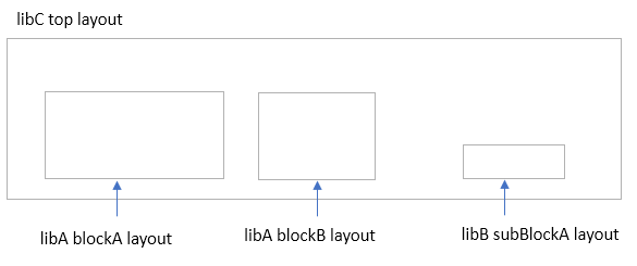
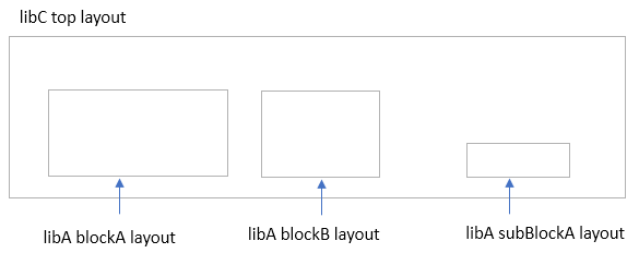
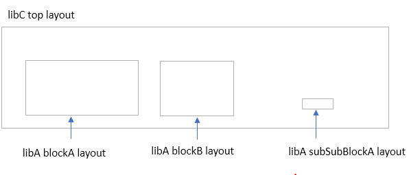
In Virtuoso, a design can have blocks specified with the same cell name but different design library names. However, if such a design is loaded into Innovus, Innovus will see both the cells as having the same design library. For example, consider a design, {libC top layout}, which contains three blocks as shown below. Two of the blocks have the same cell name blockA but are under different libraries, libA and libB.
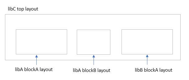
After loading the design, Innovus will read in both cells as either {libA blockA layout} or {libB blockA layout}, depending on which block it reads first.
If Innovus reads both cells as libA blockA layout, during init_design, Innovus will issue a message like the following:
**WARN: (IMPOAX-745): Cell 'blockA' from cellview 'layout' has already been read in from 'libA'. A cell can be read only once, so the second version will be ignored. Review the setting of the init_oa_ref_lib variable and update it to remove the library that has the duplicate cell.
Thus, if assembleDesign is run to flatten blockA, the flattened content of both the blocks will be the same.
18.9.8.2 assembleDesign is not able to support instances with the same cell name but different library names
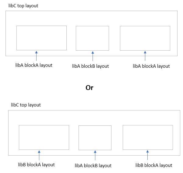
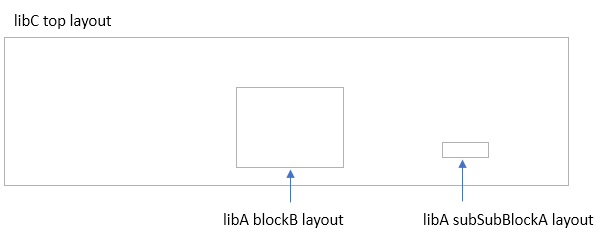
Consider a design, {libC top layout}, which contains the three blocks shown below:
Now suppose the block {libA blockA layout} contains a sub-block, {libA subBlockA layout}. This sub-block has the same cell name as the top-level block {libB subBlockA layout}. However, since the library name is different, the contents of both blocks are most likely different.
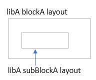
If assembleDesign is run to flatten blockA (assembleDesign -block {libA blockA layout), the resulting output will be as follows:
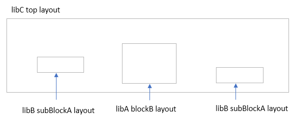
Notice that after the flattening, the cellview {libB subBlockA layout} appears in place of the cellview {libA subBlockA layout}. This is because the tool has already read in the cellview (subBlockA) earlier on during init_design and the library that it sees or binds to this cell is libB.
18.9.8.3 Handling of cells that appear at different hierarchy levels
For cellviews that are being instantiated at a different hierarchy level of a design, the sequence in which the design is assembled with assembleDesign matters in ensuring that the flattening of the design is done successfully in Innovus. To explain the concept, consider a design that has the three blocks shown below:
The cellview {libA blockA layout} contains a cellview that is the same as the one at the top, {libA subBlockA layout}. The cellview {libA subBlockA layout} in turn contains a block {libA subSubBlockA layout}.
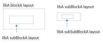
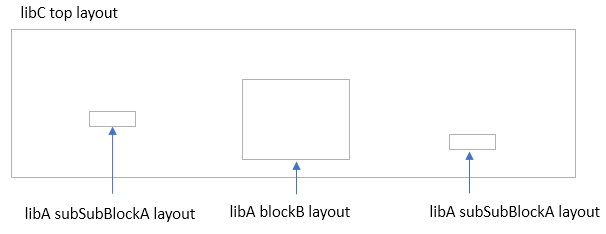
If the block {libA subBlockA layout} is flattened first (that is, the command assembleDesign -block {libA subBlockA layout} is run), the resulting output will be as follows. Notice that the cell subSubBlockA appears on the right.
However, if the following command is then run, there is nothing on the left side:
assembleDesign -block {libA blockA layout}
This is because after the first assembleDesign of {libA subBlockA layout}, a logical module of subBlockA is created. This means Innovus now interprets subBlockA as a logical module and not as a physical instance. This limitation comes from the Verilog netlist definition that Innovus used for its its logical netlist structure.
To flatten both blocks (blockA and subBlockA) correctly at the top and the child instance, the correct sequence of assembleDesign should be:
assembleDesign -block {libA blockA layout}
assembleDesign -block {libA subBlockA layout}
The resulting output is as follows:
18.10 Parasitic RC Extraction for Running MS-STA
Parasitic RC (resistance and capacitance) extraction of wiring interconnects is an important step in STA. In physical implementation, the logic instances are connected by the metal interconnects. The parasitic RC of the interconnect impacts the signal path delay. In a typical nanometer design, the parasitic RC of interconnect can account for the majority of the delay in the design.
18.10.1 Running Quantus Extraction with postRoute Engine for a Routed Design
Typically, for a design that is fully routed, the mode of extraction should be set to postRoute by specifying the following command statement:
setExtractRCMode -engine postRoute
You can use setExtractRCMode -effortLevel to further specify which extraction engine is to be used.
In the postRoute mode, -effortLevel can be specified as one of the following:
-effortLevel mediumto invoke the TQuantus extraction engine-effortLevel highto invoke the IQuantus extraction engine-effortLevel signoffto invoke the standalone Quantus extraction engine.
The TQuantus and IQuantus extraction engines are native to Innovus. To run the standalone Quantus extraction engine, the path for the Quantus binary has to be specified before invoking Innovus. All these engines require the Quantus techfile to be specified in the viewDefinition.tcl file.
18.10.2 Running Quantus Extraction with Signoff Effort Level
If the timing analysis is for signing off purpose, the -effortLevel option should be set to signoff to invoke the standalone Quantus extraction engine. The signoff effort level offers the highest level of accuracy. This is also the recommended option to handle a design that contains complex wire shapes.
The IQuantus extraction engine in Innovus is typically used for handling normal wires created by the router in the place and route environment and not for complex wires shapes that are created in Virtuoso. The following is a sample message if the design contains complex wire shapes and the effort level is not set to signoff.
**WARN: (IMPEXT-1452): Internal representation of wires of net 'por_h' at (231600 800740 3) is complex and may have overlapping geometries. So, IQuantus extraction is not possible for this net. RC estimation will be used but any SPEF that is generated subsequently will not include any RC's for this net. If this net falls in the critical path, use the signoff extractor by setting the setExtractRCMode -effortLevel to signoff for better accuracy.
Please note that if the design being analyzed contains macros that are represented as GDS because an accurate abstract is not available, the GDS representations of such macros would need to be passed to Quantus when using the Quantus integration in Innovus to perform extraction. This is done using the following settings in Innovus:
setExtractRCMode -effortLevel signoff
setExtractRCMode -coupled true
setExtractRCMode -engine postRoute
setExtractRCMode -qrcCmdType partial
setExtractRCMode -qrcCmdFile macrogds.cmd
In the above example the -qrcCmdType partial indicates that the macrogds.cmd file needs to be merged with the regular Quantus command file. The user also needs to indicate the layermap file to be used by Quantus.
18.10.3 Using the Quantus Layer Map File
This layer map is required when running the RC extraction with the signoff effort level. The layer names in the Quantus technology file may be different from the layer names used by Innovus (e.g. the layer names used in the technology file). The Quantus layer map file provides layer mapping between the technology file of Innovus and the Quantus technology file.
The following shows an example of the layer map file:
extraction_setup \
-technology_layer_map \
Metal1 METAL_1 \ Via1 VIA_1 \ Metal2 METAL_2 \ Via2 VIA_2 \ Metal3 METAL_3 \ Via3 VIA_3 \ Metal4 METAL_4 \ Via4 VIA_4 \ Metal5 METAL_5 \ Via5 VIA_5 \ Metal6 METAL_6 \ Via6 VIA_6 \ Metal7 METAL_7 \ Via7 VIA_7 \ Metal8 METAL_8 \ Via8 VIA_8 \ Metal9 METAL_9 \ Via9 VIA_9 \ Metal10 METAL_10 \ Via10 VIA_10 \ Metal11 METAL_11
Note: When the IQuantus extraction engine is selected, you do not need to specify the Quantus layer map file because Innovus will auto-create it in this mode. However, in some complex cases that have non-metal routing layer, the automatically created map file may not be correct. In such a situation, you have to specify a layer map for it.
18.10.4 Auto-creation of the Quantus Layer Map File from Innovus
To get Innovus to create a Quantus layer map file to be used or edited for other purposes (e.g. for the signoff mode), select IQuantus as the extraction engine and set the effort level to high. Then, run RC extraction.
setExtractRCMode -engine postRoute -effortLevel high
extractRC
After RC extraction is complete, look for a directory named extLogDir in the current working directory. Then look for the latest sub-directory inside the extLogDir directory (if there are multiple sub-directories). The name of the sub-directory should start with IQuantus followed by the running date, time, and so on (e.g. IQuantus_06-Jul-2017_15:16:51_18410_Q6Gdq9).
In that sub-directory, look for a file named extr.LP_pll.layermap.log. This will contain the content of the layer map that was used for running IQuantus.
18.10.5 Running Signoff Quantus Extraction in the OpenAccess Mode
By default, the signoff Quantus extraction is based on a LEF/DEF flow. To run signoff Quantus extraction in the OpenAccess mode, specify:
setExtractRCMode -useQrcOAInterface true
18.10.6 Auto-creation of Input Files from Innovus To Run Standalone Quantus QRC
During the signoff mode, Innovus generates the design input, library inputs, technology inputs and the command file to Quantus. Then it will run RC extraction in the background and read back the resulting SPEF file into Innovus. By default, the above files are stored in a temporary directory and the directory will be deleted upon completion of the whole RC extraction process.
You can use the command, write_extraction_spec to generate the command file and a directory that stores other inputs files. Use the -out_dir option to specify the directory name that stores the input files.
For example, assume the following is specified:
setExtractRCMode -engine postRoute
setExtractRCMode -effortLevel signoff
setExtractRCMode -useQrcOAInterface true
setExtractRCMode -lefTechFileMap QRC.layermap
write_extraction_spec -out_dir standalone_qrc_dir
In this case, the Quantus command file (also called the CCL file), qrc.cmd, should be generated in the working directory. In the directory named standalone_qrc_dir, you should find the input files (for example, the tech file) for Quantus QRC.
18.10.7 Running Standalone Quantus QRC and Loading the Resulting SPEF Files Back to Innovus
To run Quantus QRC in the LEF/DEF mode with qrc.def as the design input, use:
qrc -cmd qrc.cmd qrc.def
To run Quantus QRC in the OpenAccess mode, run:
qrc -qrc.cmd
The OpenAccess-mode Quantus QRC run does not require an additional design input file because the specification of the library, cell, and view names of the cellview is present in the command file, qrc.cmd.
Note: If the OpenAccess design contains PCells, Quantus requires the PCell cache, generated using Virtuoso’s Express Pcell Manager, to read in the PCells. The CDS_ENABLE_EXP_PCELL and CDS_EXP_PCELL_DIR environment variables are also consumed by Quantus for locating the PCell cache directory. For example, the following statements specify that the PCell cache is stored in the ./.expressPcells directory.
setenv CDS_ENABLE_EXP_PCELL true
setenv CDS_EXP_PCELL_DIR ./.expressPcells
To load the resulting SPEF back into Innovus (assuming two SPEF files are created for two RC corners), the commands are:
spefIn -rc_corner rc_worst LP_pll_rc_worst.spef
spefIn -rc_corner rc_best LP_pll_rc_best.spef
For more information on Quantus QRC extraction, refer to the "RC Extraction" chapter of the Innovus User Guide.
Note: In certain cases, the designs coming from Virtuoso could contain macros for which a GDS file exists, but an accurate LEF abstract is not available. If you wish to do only timing analysis at the top level, you do not need to create a detailed abstract for the macros in the design that only have GDS information. To run standalone Quantus extraction and pass the GDS representation of the macros in the design to Quantus, the following syntax needs to be used in the Quantus command file.
input_db -type oa \
 -design_cell_name <cellname> <viewname> <Design library name> \
 -library_cell_name * abstract <reference library name> \
 -gds_file_list <files containing GDS description of Macro's>\
 -library_definitions_file <the name of the cds.lib ile where libraries are defined>
Note that if -library_cell_name * abstract <reference library name> \ is not defined and -gds_file_list has been specified, Quantus will automatically use the layout view of the leaf-level cells, if available. In this case, if the layout views of the leaf-level cells have issues with pin, etc, Quantus may run into a problem and not extract certain nets.
18.11 Tips for Debugging the No Constrained Timing Path Issue Generated by report_timing
When you run report_timing, the timer may sometimes issue the following message instead of generating a timing report:
> report_timing -from wdac/a_reg/D
No constrained timing paths found. Design may not be unconstrained or library is missing timing information.
This section will help you understand what this message means, the reasons why the timer issues such a message, and the ways to debug and fix the issue. However, before you do so, it is important to review the basic conditions that must be met for the timer to generate a timing report on a path. The following case study will help you understand these conditions.
18.11.1 Case Studies
The goal is to time a path between two registers (dig/launch_reg to dig/cap_reg) inside a digital block (DIG).
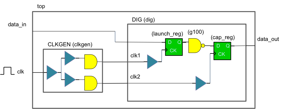
A timing constraint is specified at the primary input port (clk) of the top level design:
create_clock -name clk -period 10 [get_ports clk]
The clock signal has to propagate through a CLKGEN block before reaching the DIG block. Internally, the clock signal goes through some buffers and clock gating cells. As this is a hierarchical design, assuming the top-level design is already loaded, you need to run the assembleDesign command to flatten the CLKGEN and DIG blocks.
assembleDesign -block {designLib CLKGEN layout} -block {designLib DIG layout}
Assume that the two blocks are XL-compliant so that when they are flattened, there is logical connectivity for all instances on the clock and data paths of the two registers. With the timing library for all the standard cells loaded into the tool, the timer should see a valid path from the primary input port (clk) to both registers (dig/launch_reg to dig/cap_reg).
When the following command is run, a timing report such as the one given below is displayed:
> report_timing -from dig/launch_reg/Q -to dig/cap_reg/D
Path 1: MET Setup Check with Pin dig/cap_reg/CKEndpoint: dig/cap_reg/D (v) checked with leading edge of 'clk' Beginpoint: dig/launch_reg/Q (^) triggered by leading edge of 'clk' Path Groups: {clk} Analysis View: max Other End Arrival Time 0.437
- Setup 0.048
+ Phase Shift 10.000
= Required Time 10.389
- Arrival Time 0.818
= Slack Time 9.571
Clock Rise Edge 0.000
+ Clock Network Latency (Prop) 0.437
= Beginpoint Arrival Time 0.437
+---------------------------------------------------------------------+
| Instance | Arc | Cell | Delay | Arrival | Required |
| | | | | Time | Time |
|----------------+-------------+---------+-------+---------+----------|
| dig/launch_reg | CK ^ | | | 0.437 | 10.008 |
| dig/launch_reg | CK ^ -> Q ^ | DFFRX1 | 0.315 | 0.752 | 10.322 |
| dig/g100 | A ^ -> Y v | NAND2X1 | 0.067 | 0.819 | 10.389 |
| dig/cap_reg | D v | DFFRX1 | 0.000 | 0.818 | 10.389 |
+---------------------------------------------------------------------+
18.11.1.1 Case 1 - the create_clock constraint is specified at the wrong point
What would be the result if the create_clock statement is specified at the pin level instead of the primary port level of the DIG block? For example:
create_clock -name clk -period 10 [get_pins dig/clk1]
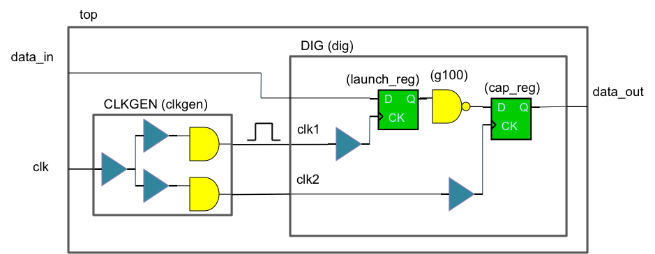
When the same path is now timed, the timer reports no constrained timing path:
> report_timing -from dig/launch_reg/Q -to dig/cap_reg/D
No constrained timing paths found. Design may not be unconstrained or library is missing timing information.
To debug the issue, run the command again with the additional option -unconstrained to check if the timer reports more information:
> report_timing -from dig/launch_reg/Q -to dig/cap_reg/D -unconstrained
The unconstrained output shown in the report indicates that something is not right at the capturing end (or the capturing clock).Path 1:Endpoint: dig/cap_reg/D (v) (unconstrained output)
Beginpoint: dig/launch_reg/Q (^) triggered by leading edge of 'clk'
Arrival Time 0.450
Analysis View: max
+ Clock Network Latency (Prop) 0.068
= Beginpoint Arrival Time 0.068
+----------------------------------------------------------+
| Instance | Arc | Cell | Delay | Arrival |
| | | | | Time |
|----------------+-------------+---------+-------+---------|
| dig/launch_reg | CK ^ | | | 0.068 |
| dig/launch_reg | CK ^ -> Q ^ | DFFRX1 | 0.315 | 0.383 |
| dig/g100 | A ^ -> Y v | NAND2X1 | 0.067 | 0.450 |
| dig/cap_reg | D v | DFFRX1 | 0.000 | 0.450 |
+----------------------------------------------------------+
In fact, its clock path is not constrained. The capturing register is not receiving a clock signal.
Now, what if the create_clock statement is specified at the other clock input of the DIG block?
create_clock -name clk -period 10 [get_pins dig/clk2]
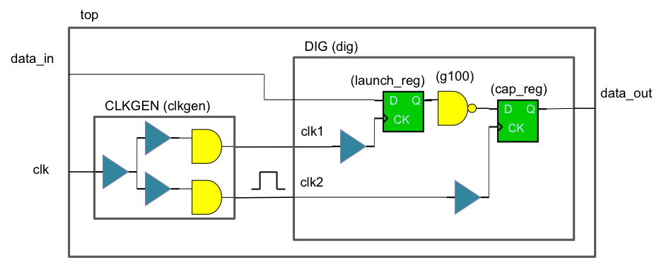
The timer reports no constrained timing path in this case as well.
> report_timing -from dig/launch_reg/Q -to dig/cap_reg/D
No constrained timing paths found. Design may not be unconstrained or library is missing timing information.
To debug, run the command again with the -unconstrained option:
> report_timing -from dig/launch_reg/Q -to dig/cap_reg/D -unconstrained
This time, the timer reports that the beginning point is not constrained.
Path 1:Endpoint: dig/cap_reg/D (v)
Beginpoint: dig/launch_reg/Q (^) (unconstrained input)
Arrival Time 0.382
Analysis View: max
+ Clock Network Latency (Ideal) 0.000
= Beginpoint Arrival Time 0.000
+----------------------------------------------------------+
| Instance | Arc | Cell | Delay | Arrival |
| | | | | Time |
|----------------+-------------+---------+-------+---------|
| dig/launch_reg | CK ^ | | | 0.000 |
| dig/launch_reg | CK ^ -> Q ^ | DFFRX1 | 0.315 | 0.315 |
| dig/g100 | A ^ -> Y v | NAND2X1 | 0.067 | 0.382 |
| dig/cap_reg | D v | DFFRX1 | 0.000 | 0.382 |
+----------------------------------------------------------+
Both these examples highlight the case where the timing path is not fully constrained.
18.11.1.2 Case 2 - the CLKGEN block is not flattened
Consider another situation in which the assembleDesign command is run only on the DIG block.
> assembleDesign -block {designLib DIG layout}
In this case, the CLKGEN block is not flattened. As a result, the actual path becomes the following:
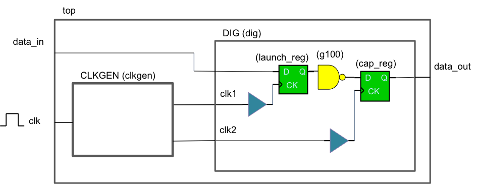
No constrained timing path will be reported if the same path is to be timed.
> report_timing -from dig/launch_reg/Q -to dig/cap_reg/D
No constrained timing paths found. Design may not be unconstrained or library is missing timing information.
Run report_timing with the -unconstrained option:
report_timing -from dig/launch_reg/Q -to dig/cap_reg/D -unconstrained
It reports that the beginning point is not constrained properly.Path 1:Endpoint: dig/cap_reg/D (v) Beginpoint: dig/launch_reg/Q (^) (unconstrained input) Arrival Time 0.381 Analysis View: max + Clock Network Latency (Ideal) 0.000 = Beginpoint Arrival Time 0.000 +----------------------------------------------------------+ | Instance | Arc | Cell | Delay | Arrival | | | | | | Time | |----------------+-------------+---------+-------+---------| | dig/launch_reg | CK ^ | | | 0.000 | | dig/launch_reg | CK ^ -> Q ^ | DFFRX1 | 0.313 | 0.313 | | dig/g100 | A ^ -> Y v | NAND2X1 | 0.068 | 0.381 | | dig/cap_reg | D v | DFFRX1 | 0.000 | 0.381 | +----------------------------------------------------------+
To further investigate whether the issue falls on the clock path, run the following command:
report_timing -unconstrained -clock_from clk
Path 1:Endpoint: clkgen/clk (v) (unconstrained output)
Beginpoint: clk (v) triggered by trailing edge of 'clk'
Arrival Time 0.000
Analysis View: max
= Beginpoint Arrival Time 0.000
+---------------------------------------------+
| Instance | Arc | Cell | Delay | Arrival |
| | | | | Time |
|----------+-------+--------+-------+---------|
| | clk v | | | 0.000 |
| clkgen | clk v | CLKGEN | 0.000 | 0.000 |
+---------------------------------------------+
The result shows that the clock propagation stops at the input of CLKGEN and is not able to reach the clock input of launch_reg and cap_reg of DIG block. In this case, the timing constraint is valid. However, the clock is not able to propagate through the CLKGEN block unless a timing library for the CLKGEN block is provided. If the CLKGEN block is flattened so that those standard cells (which have timing library loaded to the tool) on the clock path are brought to the top for timing analysis, then the path will become valid.
Use the report_instance_library command to check if an instance is bound with timing library.
> report_instance_library -instance clkgen
Instance : clkgen Analysis View : max Power Domain : - Op Cond : P->1.000000, V->0.900000, T->125.000000 (slow_oc)
The output shows that the clkgen instance is not bound with any timing library.
If a cell is bound with timing library, the name of the library file that is bound to it is displayed in the output. For example, if you run the same command for dig/launch_reg, the output is as follows:
> report_instance_library -instance dig/launch_reg
Instance : dig/launch_reg Analysis View : max Power Domain : - Library/Libset(early) : slow/slow_libset Library File (early) : gsclib045/timing/slow_vdd1v0.lib Library/Libset(late) : slow/slow_libset Library File (late) : gsclib045/timing/slow_vdd1v0.lib Op Cond : P->1.000000, V->0.900000, T->125.000000 (slow_oc) Cell Type : gateCell
Without the timing library, the timer is not able to understand the timing relationship between the input and output pins of the CLKGEN block. This example highlights one common reason why a path is viewed as an invalid or broken timing path by the timer. As a result, the timer is unable to time it.
18.11.2 Basic Conditions for Reporting the Timing on a Path
As seen in the case study, the timer can report the timing on a path only if the path is constrained with timing constraint. In other words, the following basic conditions must be met for the timer to report the timing on a path:
- The timing constraint for the path to be timed exists and is valid.
- The path covered by the constraint exists and is not broken.
So, what does the following message actually mean?
No constrained timing paths found. Design may not be unconstrained or library is missing timing information.
'No constrained timing paths' can be interpreted as either 'No constraint' or 'No timing paths'.
- 'No constraint' means that there is no valid timing constraint for the paths of concern.
- 'No timing paths' means that the paths are broken or invalid.
18.11.3 Common No Constraint Situations
Here are some common situations where the timer either cannot find a timing constraint or the timing constraint found is not valid.
18.11.3.1 No timing constraint loaded
In the assembleDesign flow, make sure that the timing constraint file is specified using create_constraint_mode in viewDefinition.tcl . The example below shows how a timing constraint file, func.sdc , is specified.
create_constraint_mode -name func -sdc_files [list func.sdc]
In the FTM flow, make sure that the timing constraint file is specified using the -ilm_sdc_files option, whether it is for the create_constraint_mode statement specified in viewDefinition.tcl, or for update_constraint_mode, which is a TCL command run after init_design. For example, if the timing constraint file name is func_flat.sdc, the statement or command should be:
create_constraint_mode -name func -sdc_files [list func_top.sdc] -ilm_sdc_files {func_flat.sdc}
update_constraint_mode -name func -ilm_sdc_files {func_flat.sdc}
Refer to the "Load the top-level design" of the Running STA by Using the FTM section for more details on the difference between top-design-only timing constraint (i.e. func_top.sdc) and flat timing constraint (i.e. func_flat.sdc). The flat type (here, func_flat.sdc) should be used for the FTM flow.
In both flows, the specified constraint mode should be tied to an analysis view and the analysis view should be specified using the set_analysis_view command. Basically, each analysis view contains a constraint mode and a delay corner. For example, to include the func constraint mode in analysis views and specify the associated analysis views for both setup and hold analysis, use the following commands:
create_analysis_view -name func_worst -constraint_mode func –delay_corner dc_worst
create_analysis_view -name func_best -constraint_mode func –delay_corner dc_best
set_analysis_view -setup [list func_worst] -hold [func_worst func_best]
18.11.3.2 No appropriate timing constraint for each type of path
Depending on the type of the path to be timed, appropriate timing constraint statement has to be specified in the timing constraint file.
Register-to-register path
At least one create_clock constraint is needed to time a register-to-register path. Typically, when the clock path involves a clock divider or clock multiplier, the create_generated_clock constraint is required.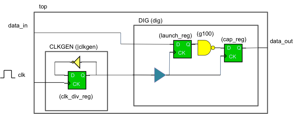
For the above diagram, the clocks can be specified as follows:
create_clock -name clk -period 10 [get_ports clk]
create_generated_clock -name clk_div -source [get_ports clk] -divide_by 2 [get_pins clkgen/clk_div_reg/Q]
Without the create_generated_clock constraint, the clock propagation stops at the CK pin of clk_div_reg and will not propagate through the Q pin of clk_div_reg.
Input-to-register path
The data arrival times should be specified at the specified input ports, relative to the clock specified by the -clock option using the set_input_delay constraint.
For example:
create_clock -name clk -period 10 [get_ports clk]
set_input_delay 2.43 -clock [get_clocks clk] [get_ports data_in]
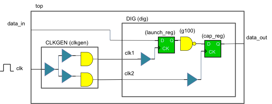
Note that, if set_input_delay is not specified, the tool is still able to report the timing, with an exception that the beginning point is not triggered by a clock (therefore, it shows @). One example is shown below:> report_timing -to dig/launch_reg/D -from data_in
Path 1: MET Setup Check with Pin dig/launch_reg/CK Endpoint: dig/launch_reg/D (^) checked with leading edge of 'clk' Beginpoint: data_in (^) triggered by leading edge of '@' Path Groups: {clk} Analysis View: max Other End Arrival Time 0.437 - Setup 0.100 + Phase Shift 10.000 = Required Time 10.337 - Arrival Time 0.000 = Slack Time 10.337 Clock Rise Edge 0.000
+ Input Delay 0.000
= Beginpoint Arrival Time 0.000 +------------------------------------------------------------------+ | Instance | Arc | Cell | Delay | Arrival | Required | | | | | | Time | Time | |----------------+-----------+--------+-------+---------+----------| | | data_in ^ | | | 0.000 | 10.337 | | dig/launch_reg | D ^ | DFFRX1 | 0.000 | 0.000 | 10.337 | +------------------------------------------------------------------+
Register-to-output path
The data required times should be specified at the specified output ports, relative to the clock specified by the -clock option using the set_output_delay constraint. For example:
create_clock -name clk -period 10 [get_ports clk]
set_output_delay 1.23 –clock [get_clocks clk] [get_ports data_out]
If set_output_delay is not specified, the timer reports no constrained timing paths found. An example is shown below:
> report_timing -from dig/cap_reg/CK -to data_out
No constrained timing paths found. Design may not be unconstrained or library is missing timing information.
To debug the issue, specify the -unconstrained option and run the command again.
> report_timing -from dig/cap_reg/CK -to data_out -unconstrained
Path 1:Endpoint: data_out (^) (unconstrained output) Beginpoint: dig/cap_reg/Q (^) triggered by leading edge of 'clk' Arrival Time 0.744 Analysis View: max + Clock Network Latency (Prop) 0.437= Beginpoint Arrival Time 0.437 +-------------------------------------------------------+ | Instance | Arc | Cell | Delay | Arrival | | | | | | Time | |-------------+-------------+----------+-------+---------| | dig/cap_reg | CK ^ | | | 0.437 | | dig/cap_reg | CK ^ -> Q ^ | DFFRX1 | 0.307 | 0.744 | | | data_out ^ | | 0.000 | 0.744 | +--------------------------------------------------------+
Combination path
A combination path involves no actual clock path. One common example of timing a combination path is to time a path from an input port to an output port that has no register in between.
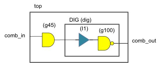
For this type of path, you can specify the set_input_delay and set_output_delay constraints with a virtual clock. A virtual clock is a clock that is not associated with any part of the design.
create_clock -name v_clk -period 10 set_input_delay 4 -clock [get_clocks v_clk] [get_ports comb_in] set_output_delay 4 -clock [get_clocks v_clk] [get_ports comb_out]
Alternatively, you may choose to specify set_max_delay to constrain such a type of path for setup time analysis and set_min_delay for hold time analysis.
set_max_delay 2 -from [get_ports comb_in] -to [get_ports comb_out] set_min_delay 1 -from [get_ports comb_in] -to [get_ports comb_out]
18.11.3.3 Design object specified in timing constraint does not match with the actual layout
A few examples of design objects are instances, primary ports, or pins of an instance. If the timer is not able to recognize a design object referenced in a timing constraint statement, that constraint statement is rejected. Some common situations are explained here:
Pipeline character in instance name of AOT design
If the top-level design is implemented in Virtuoso, the pipeline (|) character may be part of the instance name for blocks instantiated in the top-level design. In the mixed-signal OpenAccess (MSOA) flow, Innovus reads the design object from the physical layout cellview and not from the schematic cellview. If the timing constraint file is originally created based on the schematic, it may have to be modified to add | characters to the instance name to match with the corresponding name in the physical layout.
In the example below, the DIG block has been implemented in Innovus while the AMS block is a custom digital bock implemented by Virtuoso. Both blocks are integrated in Virtuoso, making it a schematic-on-top or Analog-on-Top (AOT) design.
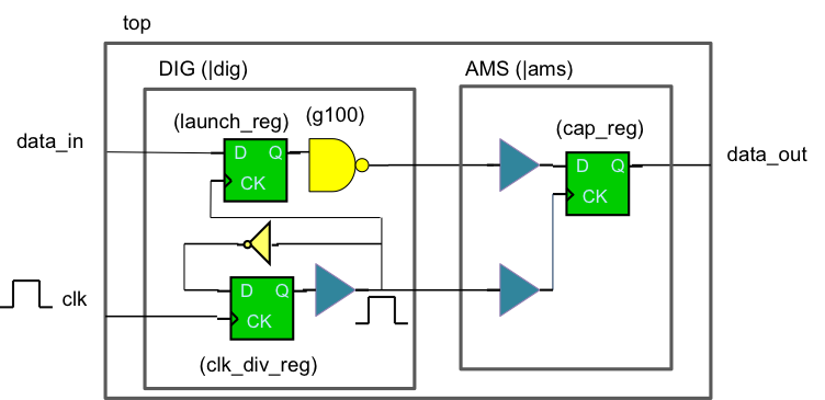
Assume the original timing constraints that are based on the schematic diagram are as follows:
create_clock -name clk -period 10 [get_pins dig/clk_div_reg/CK] create_generated_clock -name clk_div -source [get_pins dig/clk_div_reg/CK] -divide_by 2 [get_pins dig/clk_div_reg/Q]
However, to time this OpenAccess design in Innovus (or Tempus), the timing constraint should be as follows:
create_clock -name clk -period 10 [get_pins |dig/clk_div_reg/CK] create_generated_clock -name clk_div -source [get_pins |dig/clk_div_reg/CK] -divide_by 2 [get_pins |dig/clk_div_reg/Q]
Timing constraint at the wrong design level
Another reason why the design object does not match could be that the timing constraint is meant for a different design level.
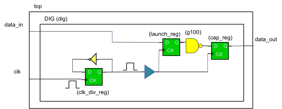
For example, for this schematic diagram, assume a timing constraint file with the following content is received from a designer:
create_clock -name clk -period 10 [get_pins clk_div_reg/CK] create_generated_clock -name clk_div -source [get_pins clk_div_reg/CK] -divide_by 2 [get_pins clk_div_reg/Q]
By examining the content, one can easily see that the constraint is specified at the DIG (dig) level and not at the top level. Probably, the designer is the designer of the DIG block.
Whether assembleDesign is run on the DIG block ( assembleDesign -block {designLib DIG layout} ) or the FTM for the DIG block is created and specified ( specifyIlm -cell DIG -dir dig_FTM ), the required timing constraints should have an additional hierarchy ( dig ) for the specified instance name.
create_clock –name clk -period 10 [get_pins dig/clk_div_reg/CK]
create_generated_clock -name clk_div -source [get_pins dig/clk_div-reg/CK] -divide_by 2 [get_pins dig/clk_div_reg/Q]
Block not flattened or FTM not specified
Consider the case below:
create_clock -name clk -period 10 [get_pins clkgen/clk_div_reg/CK]
create_generated_clock -name clk_div -source [get_pins clkgen/clk_div_reg/CK] -divide_by 2 [get_pins clkgen/clk_div_reg/Q]

Here, the timing constraints are correct. However, if the CLKGEN block is not flattened using assembleDesign or an FTM is not created and specified for it, the diagram look likes the following and the timer does not accept these timing constraint statements. This is because the timer cannot find any instance in the physical layout cellview with name equal to clkgen/clk_div_reg .
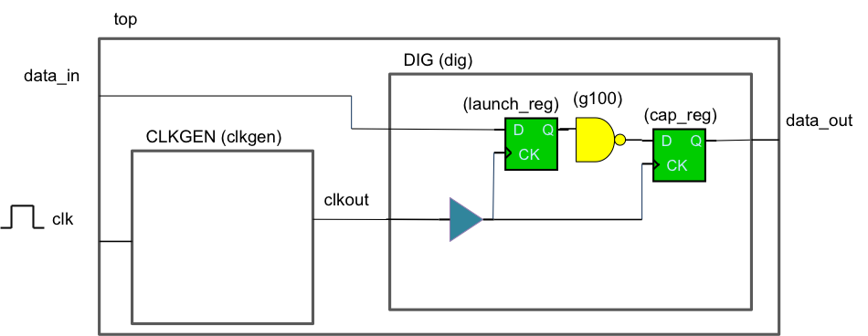
The workaround is to either get a timing library for the CLKGEN block (which takes more effort and time) or modify the timing constraint as follows:
create_clock -name clk -period 20 [get_pins clkgen/clkout]
18.11.4 Checking the Validity of a Timing Constraint
How can you check whether a timing constraint is valid or, in other words, acceptable to the timer?
You can look at the log file and search for the timing constraint file name. When the timer parses a timing constraint file and detects something wrong with the constraints, it will issue warnings or errors in the log file.
Let us use the previous case again to illustrate how you can check the validity of the timing constraints.
The timing constraints are:
create_clock -name clk -period 10 [get_ports clk]
create_generated_clock -name clk_div -source [get_ports clk] -divide_by 2 [get_pins clkgen/clk_div_reg/Q]
Assume these constraints are specified in a file called simple.sdc, and this timing constraint file is specified in viewDefinition.tcl.
18.11.4.1 Successful case for the assembleDesign flow
Assume the assembleDesign flow is run for the above case and the script is as follows:
set_db init_design_netlisttype {OA}set_db init_oa_design_lib {designLib}set_db init_oa_design_cell {top}set_db init_oa_design_view {layout}set_db init_oa_ref_lib {gsclib045}set_db init_mmmc_file {viewDefinition.tcl}
init_design
setExtractRCMode -engine postRoute
setExtractRCMode -effortLevel high
assembleDesign -block {designLib DIG layout} -block {designLib CLKGEN layout}
source viewDefinition.tcl
Now, when you search for simple.sdc in the log file, you should see something like the following:
CTE reading timing constraint file 'simple.sdc' ...
Note - Ignore the message that is issued during init_design. At this point in time, errors related to timing constraints are expected because the CLKGEN block is not yet flattened. Therefore, the tool cannot find objects such as clkgen/clk_div_reg/Q in the layout.
To check whether the timing constraints are accepted by the timer, you can run source viewDefinition.tcl after assembleDesign is done.
If the constraints are read successfully, it should show something like the following:
CTE reading timing constraint file 'simple.sdc' ... Current (total cpu=0:00:19.5, real=0:01:16, peak res=325.1M, current mem=660.9M) INFO (CTE): Constraints read successfully.
18.11.4.2 Unsuccessful case for the assembleDesign flow
Now, suppose the assembleDesign command is run as follows:
assembleDesign -block {designLib DIG layout} source viewDefinition.tcl
As the CLKGEN block is not flattened, the timer reports errors on the timing constraints when the viewDefinition.tcl is sourced again after assembleDesign.
CTE reading timing constraint file 'simple.sdc' ... Current (total cpu=0:00:08.5, real=0:00:15.0, peak res=201.2M, current mem=544.5M) **WARN: (TCLCMD-513): The software could not find a matching object of the specified type for the pattern 'clkgen/clk_div_reg/Q' (File simple.sdc, Line 2). **ERROR: (TCLCMD-917): Cannot find 'pins' that match 'clkgen/clk_div_reg/Q' (File simple.sdc, Line 2). **ERROR: (TCLCMD-917): Cannot find 'ports or pins' that match '' (File simple.sdc, Line 2). INFO (CTE): read_dc_script finished with 1 WARNING and 2 ERROR.
18.11.4.3 Successful case for the FTM flow
Assume the FTM flow is run for the same case and the script is as follows:
set_db init_design_netlisttype {OA}set_db init_oa_design_lib {designLib} set_db init_oa_design_cell {top} set_db init_oa_design_view {layout} set_db init_oa_ref_lib {gsclib045} set_db init_mmmc_file {viewDefinition.tcl}
init_design
setExtractRCMode -engine postRoute
setExtractRCMode -effortLevel high
specifyIlm -cell DIG -dir dig_FTM
specifyIlm -cell CLKGEN -dir clkgen_FTM
flattenIlm
update_constraint_mode -name func -ilm_sdc_files {simple.sdc}
Assume the timing constraint mode specified in viewDefinition.tcl is created as follows:
create_constraint_mode -name func -sdc_files [list simple.sdc]
When looking at the log file,ignore the errors and warning reported by the timer during init_design. At this point of time, the tool is not able to see any internal content inside the CLKGEN block and, therefore, is expected to report errors. Look at the lines after create_constraint_mode and the constraints should have been read successfully.
<CMD> update_constraint_mode -name func -ilm_sdc_files {simple.sdc} CTE reading timing constraint file 'simple.sdc' ... Current (total cpu=0:00:13.2, real=0:00:17.0, peak res=316.0M, current mem=636.9M) INFO (CTE): Constraints read successfully.
Note that the command update_constraint_mode is not necessary if the -ilm_sdc_files option is already specified in the timing constraint mode in viewDefinition.tcl as follows:
create_constraint_mode -name func -sdc_files [list simple.sdc] -ilm_sdc_files {simple.sdc}
Then, check whether constraints are read successfully during the command flattenIlm.
<CMD> flattenIlm Reading one ILM netlist ...
... CTE reading timing constraint file 'simple.sdc' ... Current (total cpu=0:00:11.9, real=0:00:17.0, peak res=305.0M, current mem=632.3M) INFO (CTE): Constraints read successfully.
18.11.4.4 Unsuccessful case for FTM flow
If you have specified the FTM only for the DIG block, the timer will report errors on the timing constraint when the flattenIlm or update_constraint_mode commands are run.
specifyIlm -cell DIG -dir dig_FTM #specifyILM -cell CLKGEN -dir clkgen_FTM flattenIlm
CTE reading timing constraint file 'simple.sdc' ... Current (total cpu=0:00:08.5, real=0:00:15.0, peak res=201.2M, current mem=544.5M) **WARN: (TCLCMD-513): The software could not find a matching object of the specified type for the pattern 'clkgen/clk_div_reg/Q' (File simple.sdc, Line 2). **ERROR: (TCLCMD-917): Cannot find 'pins' that match 'clkgen/clk_div_reg/Q' (File simple.sdc, Line 2). **ERROR: (TCLCMD-917): Cannot find 'ports or pins' that match '' (File simple.sdc, Line 2). INFO (CTE): read_dc_script finished with 1 WARNING and 2 ERROR.
18.11.5 Checking the Existence of a Design Object in the Layout
When a timing constraint is not accepted by the timer because a design object is not found, how can you verify that the specified design object exists in the design layout? Or if there is a typo in the object name specified, how can you find the right name of the object?
In the above example, the tool returns the following message when reading the timing constraint:
**WARN: (TCLCMD-513): The software could not find a matching object of the specified type for the pattern 'clkgen/clk_div_reg/Q' (File simple.sdc, Line 2).
To check if the object clkgen/clk_div_reg exists in the design, open the Design Browser from the Tools menu in Innovus. You can use the * character as a wild card.
Note - The Design Browser verification has to be done after the blocks are flattened. A block that has not been flattened is viewed as a blackbox logically by the tool.
In the following screenshot, *clkgen/*reg* is entered in the Design Browser and it shows up all instances that match with the input.
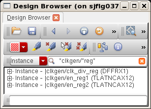
After checking the Design Browser and examining the simple.sdc file, you can see that the design object is not specified correctly in the following constraint:
create_generated_clock -name clk_div -source [get_ports clk] -divide_by 2 [get_pins clkgen/clk_div_reg/Q]
It should be:
create_generated_clock -name clk_div -source [get_ports clk] -divide_by 2 [get_pins |clkgen/clk_div_reg/Q]
18.11.6 Common Invalid Timing Path Situations
Here are some common situations that could cause the timing path to be invalid. In each case, either the timing library is not present or the signal propagation is blocked.
18.11.6.1 Block not flattened or FTM not read
The diagram below shows a case where the data path is broken. The timing constraint is:
create_clock -name clk -period 10 [get_ports clk]
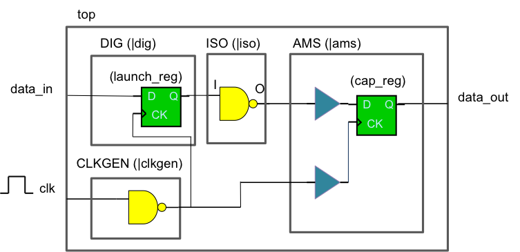
Assume the timing library for all the above standard cells is available and loaded. In the above case, either assembleDesign has to be run or FTM has to be specified for the DIG , CLKGEN , ISO and AMS blocks to report the timing between the two registers.
However, if the ISO block that contains the isolation cells (assuming this is a low power design) is not flattened or its FTM is not specified, the path is viewed by the timer as follows:
As a result, the timer will report an unconstrained timing path if you run report_timing on the path:
> report_timing -from dig/launch_reg/Q -to dig/cap_reg/D
No constrained timing paths found. Design may not be unconstrained or library is missing timing information.
To further investigate whether the propagation of the data signal stops at ISO cell, you can run the following:
> report_timing -from dig/launch_reg/Q -to dig/iso/I -unconstrained Path 1:Endpoint: dig/cap_reg/D (v) (unconstrained output) Beginpoint: dig/launch_reg/Q (^) triggered by leading edge of 'clk' Arrival Time 0.383 Analysis View: max + Clock Network Latency (Prop) 0.068 = Beginpoint Arrival Time 0.068 +----------------------------------------------------------+ | Instance | Arc | Cell | Delay | Arrival | | | | | | Time | |----------------+-------------+---------+-------+---------| | dig/launch_reg | CK ^ | | | 0.068 | | dig/launch_reg | CK ^ -> Q ^ | DFFRX1 | 0.315 | 0.383 | | dig/iso | I ^ | ISO 1 | 0.000 | 0.383 | +----------------------------------------------------------+
The above report shows that the propagation of the data path stops at the input of the ISO cell, resulting in a broken path.
18.11.6.2 Cell not bound with timing library
When timing a path, the timer needs to understand the function and delay attributes of all leaf cells along the timing path. Therefore, all these leaf cells must have timing library representation. Typically, the issue of cell not bound with timing library occurs when the library set is not specified with a complete set of library files in the viewDefinition.tcl file.
For example, for designs with multiple timing library files, especially ones with multiple power domains (e.g. with different sets of supply voltages, or threshold voltages, for specific low power cells), a certain amount of effort and time is required to find out all the necessary timing library files to be loaded into the tool. Therefore, it is possible that in the first few runs of timing analysis, some of the timing library files are left out and not specified in the viewDefinition.tcl file.
To debug if a cell is bound with the timing library, run report_instance_library with the instance name specified.
The example below shows that the instance dig/ram4k is not bound with the timing library.
report_instance_library -instance dig/ram4k
Instance : dig/ram4k Analysis View : max Power Domain : - Op Cond : P->1.000000, V->0.900000, T->125.000000 (slow_oc)
The example below shows that the instance dig/ram4k is bound with two timing library files, custom_best.lib and custom_worst.lib.
report_instance_library -instance dig/ram4k
Instance : dig/ram4k Analysis View : max Power Domain : - Library/Libset(early) : custom/1v32_min Library File (early) : /lib/custom_best.lib Library/Libset(late) : custom/1v08_max Library File (late) : /lib/custom_worst.lib Op Cond : P->1.000000, V->0.900000, T->125.000000 (slow_oc)
The following options suggest how the library set should be specified in the viewDefinition.tcl file for two specific situations:
Cell exists only inside a flattened block
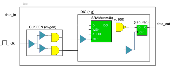
In the above case, suppose you want to time the path from dig/ram4k/DO to dig/cap_reg/D. Assume the library information is as follows:
- The timing library model for the SRAM cell is contained in a file called
sram.lib. - The timing library model for all other standard cells is
slow.lib. - The physical library that stores the abstract cellview for the standard cells is
gsclib045.
Specify all the timing library files, including the ones that have cells appearing only in the blocks to be flattened (e.g. SRAM), in the viewDefinition.tcl file:
create_library_set -name lib_worst -timing [list lib/slow.lib lib/sram.lib]
The following is a sample script to run the flattened flow.
set_db init_design_netlisttype {OA}set_db init_oa_design_lib {designLib}set_db init_oa_design_cell {top}set_db init_oa_design_view {layout}set_db init_oa_ref_lib {gsclib045}set_db init_mmmc_file {viewDefinition.tcl}
init_design
setExtractRCMode -engine postRoute
setExtractRCMode -effortLevel high
assembleDesign -block {designLib DIG layout} -block {designLib CLKGEN layout}
report_timing -from dig/ram4k/DO -to dig/cap_reg/D
Cell exists only inside an FTM block
Similarly, in the FTM flow, specify all the timing library files in the viewDefinition.tcl upfront. An example is shown below:
create_library_set -name lib_worst -timing [list lib/slow.lib lib/sram.lib]
A sample script for the FTM flow is shown below:
set_db init_design_netlisttype {OA}set_db init_oa_design_lib {designLib}set_db init_oa_design_cell {top}set_db init_oa_design_view {layout}set_db init_oa_ref_lib {gsclib045}set_db init_mmmc_file {viewDefinition.tcl}
init_design
specifyILM -cell DIG -dir dig_FTM
setExtractRCMode -engine postRoute -effortLevel high
flattenILM
update_constraint_mode -name func -ilm_sdc_files {simple.sdc}
report_timing -from dig/ram4k/DO -to dig/cap_reg/D
18.11.6.3 Bad timing library
The cell is bound with the timing library but the timing description in the timing library is incomplete. For example, the following cell appears to be a buffer or inverter but the pin's specification has no timing arc description:
pin(A) { direction : input; capacitance : 0.008908; }
pin(Y) { direction : output; capacitance : 0.0; }
A proper specification for pin Y should describe its function and relationship to a particular input pin and should contain timing sense description that talks about unateness and timing look up tables for cell rise delay, rise transition, cell fall delay, and fall transition. A simple example is shown below.
pin(Y) { direction : output; output_signal_level : RAIL_VDD; capacitance : 0; max_capacitance : 0.507904; function : "A"; timing() { related_pin : "A"; timing_sense : positive_unate; cell_rise(delay_template_2x2) { index_1 ("0.008, 0.28"); index_2 ("0.01, 0.45"); values ( \ "0.079673, 0.877286", \ "0.178436, 0.976339"); } rise_transition(delay_template_2x2) { index_1 ("0.008, 0.28"); index_2 ("0.01, 0.45"); values ( \ "0.056876, 1.66719", \ "0.060035, 1.66718"); }
cell_fall(delay_template_2x2) { index_1 ("0.008, 0.28"); index_2 ("0.01, 0.45"); values ( \ "0.079517, 0.996017", \ "0.174628, 1.09146"); }
fall_transition(delay_template_7x7) { index_1 ("0.008, 0.28"); index_2 ("0.01, 0.45"); values ( \ "0.060737, 1.87573", \ "0.063819, 1.8791"); } } }
18.11.6.4 Logical connectivity issue in the path
Typically, a logical connectivity issue occurs when the design or the block to be timed is not Virtuoso XL-compliant. Refer to the Requirements for Correct Connectivity Propagation section for details on connectivity propagation. Note that the logical connectivity issue is different from the physical connectivity issue. A physical connectivity issue can be as simple as a net not routed or the wire not touching the pin shape of a cell, causing it to be an open violation. However, a logical connectivity issue refers to, for example, the tool not being able to see any logical connection between two blocks. This could be because one of the blocks has no terminals or has terminals that have been left dangling logically, even though wires are physically connecting the two blocks.
Note: To avoid misunderstanding, this section uses the word "terminal" to refer to the input or output of a cell. In static timing analysis, the input or output of a cell is often referred as a "pin" or "port". In Virtuoso, the "pin" usually refers to the physical pin shape while "terminal" refers to the corresponding logical port.
To check for logical connectivity issue, you can:
- Open Design Browser from the Tools menu in Innovus to check if the input or output of an instance is connected as expected.
- Dump out a verilog netlist in Innovus using the
saveNetlistcommand and view the content of the Verilog file to check the connection of the instances, - Load the top-level design in Virtuoso, select the instance, and select Connectivity -> Nets -> Propagate… from the top pull-down menu to view the logical connectivity of the terminals.
The following situations could lead to a logical connectivity issue in the path:
Terminal not connected or shape having no connectivity
Typically, this issue occurs because the physical wire does not have an associated net name. In Virtuoso, it is usually referred as shape having no connectivity.
In the following case, a logical connectivity issue exists at the top-level net, clk_out1, which is viewed as a floating net in Innovus.
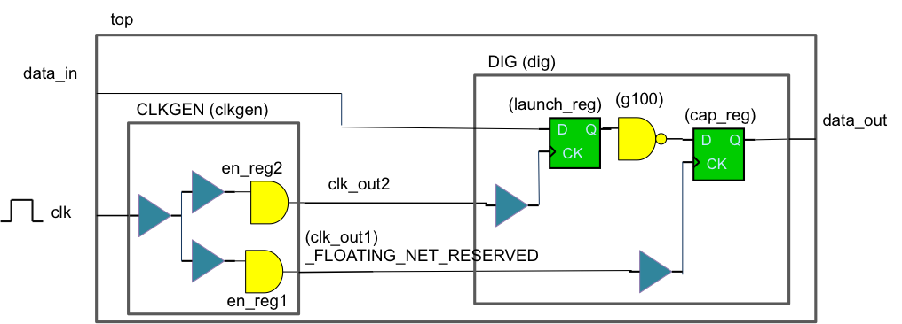
When you select the floating net in Innovus (left-click the wire) and view its attributes (press q), it is displayed as FLOATING_NET_RESERVED.
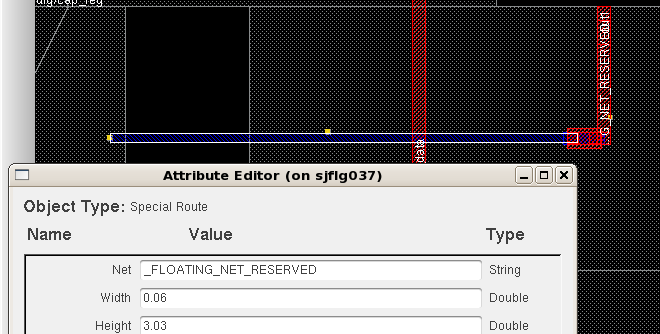
When you view the netlist or check in Design Browser, the output of the clkgen/en_reg1 instance appears to be dangling.
module top ... CLKGEN clkgen (.clk_out2(clk_out2), .clk(clk)); ... endmodule
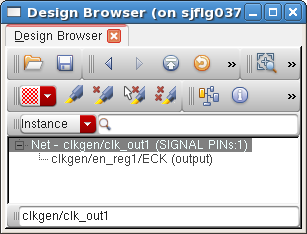
However, as can be seen in the following screenshot, the output of the clkgen/en_reg2 is connected to the top level net, clk_out2.
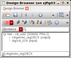
If you open the top-level design in Virtuoso and select the CLKGEN block, and then select Connectivity -> Nets -> Propagate… from the top pull-down menu, the following information can be seen:
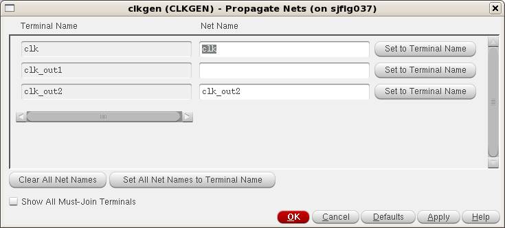
In some cases, it could be that none of the terminals are connected, and the netlist displays as follows:
module top CLKGEN clkgen (); ... endmodule
In this case, when you open the top-level design in Virtuoso and select the CLKGEN block, and then select Connectivity -> Nets -> Propagate… from the top pull-down menu, the following information can be seen:
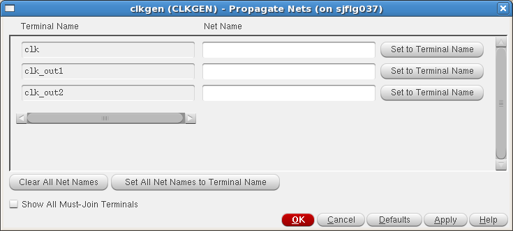
Such a situation could happen if the block is imported to Virtuoso from a GDSII file (which has no connectivity information). Typically, for a block imported through GDSII, the content of the Verilog netlist generated from the block has the following characteristics:
- The instance name starts with
I__xxxx,xxxxare numbers. - No logical connection exists between instances.
An example is shown below:
SDFFSHQX2 I__1729 (); TLATNX1 I__1730 (); TLATNX1 I__1731 (); AOI222X1 I__1732 (); ...
Missing terminal
In the previous case, the block has terminals but the terminals are dangling. In this case, the block to be assembled has no terminals at all. This is another example of non-compliance of Virtuoso XL. To check if a cell has a terminal in Innovus, select the instance in the Innovus main window and open Design Browser from the Tools menu. Alternatively, just open the Design Browser and enter the cell name.
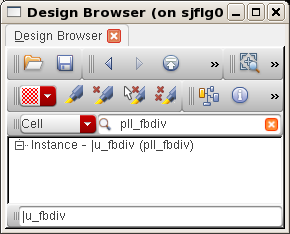
Here, the cell pll_fbdiv has no terminals. In contrast, the cell pll_reg in the screenshot below has several terminals.
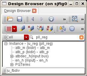
Remember to click the + symbol to the left of Instance to check if terminals exist for the cell. The + symbol becomes - when expanded.
18.11.6.5 Path not to be timed
In this case, the path is intended to be unconstrained, either by definition in the timing library or in the timing constraint file. Some situations where an unconstrained path may be used are listed below:
False path
A false path is a timing path that is not required to meet its timing constraints for the design to function properly. One typical example is an asynchronous path between multiple clocks.
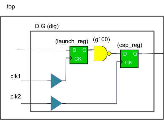
In the timing constraint file, the constraints are as follows:
create_clock -name clk1 -period 10 [get_pins dig/clk1] create_clock -name clk2 -period 10 [get_pins dig/clk2] set_false_path -from [get_clocks clk1] -to [get_clocks clk2]
> report_timing -from dig/launch_reg/Q -to dig/cap_reg/D
No constrained timing paths with given description found. Paths may be unconstrained (try '-unconstrained' option) or may not exist.
To look for these kind of false paths, you can run report_path_exceptions:
> report_path_exceptions
+---------------------------------+ | From | To | Late | View | | | | | Name | |--------+--------+-------+-------| | "clk1" | "clk2" | false | max | +---------------------------------+
Disabled timing arcs
Static timing analysis uses timing arcs to describe the cell delay from each input to each output, and the constraints between input pins. Disable a timing arc breaks a specific timing path. When a pin on a cell get disabled, all timing arcs from or to that pin is disabled. The timing arc or pin on a cell can be disabled by timing constraint, constant propagation during timing analysis, or by the timing library.
Examples of timing constraints that disable timing arcs are set_disable_timing, set_case_analysis, and set_disable_clock_gating_check.
Innovus provides TCL commands, such as
report_inactive_arcs
and
report_case_analysis
, to help you analyze such kinds of timing exceptions.
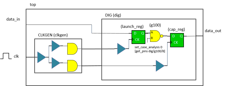
For the above example, assume the following constraints are specified in the timing constraint file:
create_clock -name clk -period 10 [get_ports clk]
set_case_analysis 0 [get_pins dig/g100/B]
> report_timing -from dig/launch_reg/Q -to dig/cap_reg/D
No constrained timing paths with given description found. Paths may be unconstrained (try '-unconstrained' option) or may not exist.
When you run report_inactive_arcs and report_case_analysis, the following reports are generated:
> report_inactive_arcs -type const
+----------------------------------------------------------------------------------+
| From | To | ArcType | Sense | Reason | View |
|------------+------------+---------------+----------------+----------------+------|
| dig/g100/A | dig/g100/Y | combinational | negative_unate | dig/g100/Y = 1 | max |
| dig/g100/B | dig/g100/Y | combinational | negative_unate | dig/g100/B = 0 | max |
+----------------------------------------------------------------------------------+
> report_case_analysis
               +-------------------------------+
  |  Pin name  |   User   | View  |
  |            |   case   | Name  |
  |            | analysis |       |
  |            |   value  |       |
  |------------+----------+-------|
  | dig/g100/B | 0        | max   |
  +-------------------------------+
For the following example which is due to constant propagation, use report_inactive_arcs because report_case_analysis reports disabled arcs only for case analysis.
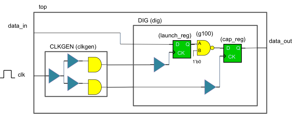
The timing constraint is:
create_clock -name clk -period 10 [get_ports clk]
> report_timing -from dig/launch_reg/Q -to dig/cap_reg/D
No constrained timing paths with given description found. Paths may be unconstrained (try '-unconstrained' option) or may not exist.
When you run report_inactive_arcs, the following reports are generated.
> report_inactive_arcs -type const
+----------------------------------------------------------------------------------+
| From | To | ArcType | Sense | Reason | View |
|------------+------------+---------------+----------------+----------------+------|
| dig/g100/A | dig/g100/Y | combinational | negative_unate | dig/g100/Y = 1 | max |
| dig/g100/B | dig/g100/Y | combinational | negative_unate | dig/g100/B = 0 | max |
+----------------------------------------------------------------------------------+
> report_case_analysis
report_case_analysis does not report anything because there is no set_case_analysis statement in the timing constraint.