4
Checking Electrical Rules (ERC)
This chapter discusses Electrical Rules Checking in Dracula, focusing on the following topics:
Electrical Rules Checker
The Dracula Electrical Rules Checker (ERC) checks for electrical rule violations. ERC isolates the exact locations at which shorts occur, eliminating the time-consuming process of finding shorts between global signals. ERC detects the following kinds of errors:
This chapter describes the ERC commands and shows detailed examples of the commands used in an ERC run. This chapter also describes hierarchical ERC (HERC).
ERC Commands
The ERC Input-Layer block commands CONNECT-LAYER and TEXTSEQUENCE determine the mask order of conductor layers and the order in which Dracula attaches text. For details about how Dracula handles text, see
The ERC Operation block commands can be grouped into the following three categories:
For details about each of the Operation block commands, refer to
Electrical Node Extraction Commands
The electrical node extraction commands define the connectivity between layers where the connection physically derives from the contacts. The CONNECT-LAYER command in the Input-Layer block defines the sequence. You define the contacts that connect the prescribed layers in the Operation block.
Electrical nodes are formed by the layer processing sequence and the interlayer contacts. Dracula forms and uniquely labels each electrical node formed by the CONNECT-LAYER and CONNECT commands. This process is called “stamping.” Dracula can carry the stamping information to newly generated layers in two ways:
- Dracula automatically stamps layers produced by the AND and NOT commands. Dracula stamps the output layer with the node label of the first specified layer.
- The STAMP command stamps the node labeling from one layer to another. Stamping occurs only for stamped layer polygons that overlap nodes in the stamping layer.
Circuit Element Extraction Commands
The circuit element extraction commands extract MOS devices, pads, and electrical parameters such as widths and lengths. When you define electrical nodes with the CONNECT command, the circuit element extraction commands automatically generate a circuit netlist. You can use this extracted circuit for ERC, LPE, and LVS operations.
Dracula checks the devices defined by ELEMENT commands to verify that the devices are correctly formed. If the terminals of a device are missing or not formed properly, Dracula reports the coordinates of the device in the .ERC file.
Electrical Rules Checking Commands
The electrical rules checking commands check for incorrect devices and gross continuity errors. Some of these rules are global and some are local.
After completing your ERC checks, Dracula flags electrical nodes and elements as potential violations and generates graphic output. For electrical nodes, Dracula traces continuity through the contacts to all areas of layers with the same electrical potential. Dracula uses a definition area to identify elements. For example, the channel area can represent the MOS device to help locate specific violations.
Because ERC operates on the internal data structure that represents the layout by trapezoids, and not polygons, the graphic output and the original layout might look different even though the covered area is the same. If multiple layers are involved in a violation, Dracula assigns consecutive output layer numbers with the lowest number being the one you specify in the command. In the following example, the MULTILAB command outputs errors to layer 50.
* INPUT-LAYER
;
diff      =  1          ; Diffusion input layer
epi       =  4          ; Epi-contact input layer
poly      =  5          ; Polysilicon input layer
cont      =  6          ; Metal-contact input layer
metal     =  7 TEXT 60  ; Metal input layer
vapox     =  8          ; VAPOX input layer for pads
natural   =  9          ; Natural XTOR implant layer
harddep   =  10         ; Hard depletion XTOR implant
softdep   =  11         ; Soft depletion XTOR implant
TEXT      =  60         ; Text layer
;
CONNECT-LAYER = srcdrn poly metal
*END
*OPERATION
CONNECT metal poly by mc
CONNECT metal srcdrn by mc
MULTILAB OUTPUT mullab 50
*END
Because multiple layers are involved, Dracula assigns graphic output layers as follows:
metal    to  layer  50
poly     to  layer  51
srcdrn   to  layer  52
mc       to  layer  53
ERC Output
ERC summaries are put in a file with a.ERC extension and the same root name as the.SUM file. The.ERC file contains the number of nodes and regions and all successfully attached text information, including the text name, its coordinate, node number, and text type. The file also records text not attached to any layer, text that caused open or short circuits, soft connection violations, and all ERC results.
To do electrical rules checks, ERC uses electrical nodes derived from the layout and text input through your CAD system, EDTEXT, or both. If your ERC run generates error output cells from MULTILAB or SAMELAB commands, you must resolve these errors before inspecting any other output.
Before loading the graphic error output cells onto your CAD system:
- Inspect module IDLAB, which is the entire text/label read in. Check the conversion of label names and their x,y coordinates.
-
Inspect module POSATT, which is the text/label processed for attachments. Dracula groups together text that must be attached to particular conductor layers by CONNECT-LAYER and lists these attachments in the far right column. The attachment might indicate whether the x,y coordinates of the text are correct. Node numbers are also listed.
POSATT shows which group of text/labels is shorted to each other (MULTILAB) and which group of text/labels is opened (SAMELAB). You find these groups listed under the warning in the.ERC summary file. - Find the layer assignment by searching for the error output name, such as SHORTS40 or OPENS40. Because MULTILAB and SAMELAB both output nodes, the error output cell layer assignments are listed under the ERC checks in the.ERC summary file.
The following is an abbreviated example of a .ERC summary file.
ERC Examples
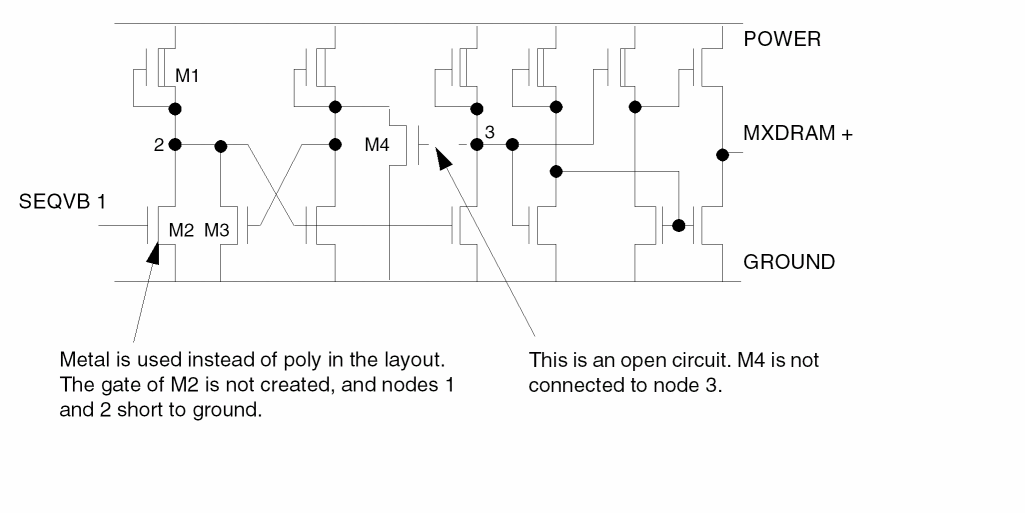
This section shows an input file that demonstrates the operation and features of ERC. One cell of a 3.5-micron NMOS technology memory chip is used for these examples. The following figure shows the layout and schematic of this cell.
For information about debugging an ERC run, refer to
Description Block
In the Description block, you define the input or output devices and file names, CAD layout graphics system, graphics unit scale factor, cell (or portion of cell), and execution mode.
*DESCRIPTION
;
PRIMARY      =  demo       ; Primary cell name
SYSTEM       =  GDS2       ; CAD graphics system
INDISK       =  demoerc    ; Input file name
OUTDISK      =  demout     ; Output file name
SCALE        =  0.001 mic  ; Graphics scale factor
PRINTFILE    =  ercprt     ; Output print file
MODE         =  exec now   ; Execution mode
RESOLUTION   =  0.125 mic  ; Minimum layout increment
;
; *END
The statistics of the memory cell in this example are as follows:
Technology            =   3.5-micron NMOS
Number of transistors =   14
CAD graphics system   =   GDS II
Graphics unit scale   =   0.001 micron
Input Layer Block
In the Input-Layer block, you correlate the layout layer number with your own symbolic name and define the mask sequence for the major layers in the technology process.
* INPUT-LAYER
;
diff      =  1          ; Diffusion input layer
epi       =  4          ; Epi-contact input layer
poly      =  5          ; Polysilicon input layer
cont      =  6          ; Metal-contact input layer
metal     =  7 TEXT 60  ; Metal input layer
vapox     =  8          ; VAPOX input layer for pads
natural   =  9          ; Natural XTOR implant layer
harddep   =  10         ; Hard depletion XTOR implant
softdep   =  11         ; Soft depletion XTOR implant
TEXT      =  60         ; Text layer
;
CONNECT-LAYER  =  srcdrn poly metal ;Layer process order
;
*END
The reverse order of the CONNECT-LAYER sequence is the default TEXTSEQUENCE that is used to attach text to the layout, that is, to metal, then to poly, and then to surgery.
Operation Block
You specify your electrical rules in the Operation block. The following example describes the set of rules you need to comply with ERC specifications.
*OPERATION
;
; ***ELECTRICAL NODE DESCRIPTION***
;
; FORM TRANSISTORS
;
AND   poly     diff     podiff
;
NOT   podiff   epi      xtor
;
OR    harddep  softdep  depl
OR    natural  depl     eblk
;
AND   xtor     depl     chnld
AND   xtor     natural  chnln
NOT   xtor     eblk     chnle
;
; FORM SOURCE-DRAIN LAYER
;
NOT   diff     xtor     srcdrn
;
; ELECTRICAL NODE CONSTRUCTION
;
; FORM PAD WINDOWS
;
AND        metal    vapox   padwin
CONNECT    metal    poly    BY cont
CONNECT    metal    srcdrn  BY cont
CONNECT    poly     srcdrn  BY epi
;
; ***NETWORK CONSTRUCTION***
;;
; FORM NETWORK
;
ELEMENT    MOS[D]   chnld   poly    srcdrn
ELEMENT    MOS[N]   chnln   poly    srcdrn
ELEMENT    MOS[E]   chnle   poly    srcdrn
ELEMENT    PAD      padwin  metal
;
; ***ELECTRICAL RULE CHECKS***
;
PROBE      vcc      OUTPUT  vcc     50
PROBE      vss      OUTPUT  vss     50
;
MULTILAB   OUTPUT   shorts  50
;
SAMELAB    OUTPUT   opens   50
;
PATHCHK    LEVEL 1  OUTPUT  path1r  50
PATHCHK    LEVEL 2  OUTPUT  path2r  50
PATHCHK    LEVEL 3  OUTPUT  path3r  50
;
ELCOUNT    mos      all     EQ 0    OUTPUT  float   50
;
NDCOUNT    mos      all     EQ 1    OUTPUT  mosnil  40
NDCOUNT    mos      srcdrn  EQ 1    OUTPUT  moscap  40
;
ECONNECT   mos[D]   srcdrn CONN vss OUTPUT  mdconn  40
; *END
After you create the Description, Input-Layer, and Operation blocks, you can store the blocks in one or more files, such as the following:
Description block   ercdesc.com
Input-Layer block   ercinpl.com
Operation block     ercoper.com
You can read these files into the preprocessor with the following commands:
/GET ercdesc NOLIST
/GET ercinpl NOLIST
/GET ercoper NOLIST
/FINISH
NMOS ERC Rules File
The following sample input file is for NMOS circuits. Because ERC checks for standard MOS digital circuit designs, some of the ERC checks are not useful for memory or linear circuits.
;********************************************************
;              SILICON GATE NMOS ERC CHECKS
;        FOR STANDARD DIGITAL DESIGN TECHNIQUES
;******************************************************** ;
;
*DESCRIPTION
;
INDISK = inchip  ; Graphic database file
OUTDISK = ercout  ; Graphic error database file
PRIMARY = top  ; Top cell name
MODE = exec now  ; Mode execution
SYSTEM = gds2  ; Graphic CAD database format
PROGRAM-DIR = drac:  ; Program directory of Dracula modules
SCALE = .001 micron  ; Graphic database scale factor
RESOLUTION = .5 micron  ; Graphic digitized grid increments
PRINTFILE = ercprt  ; Print-file name ERC run
;
*END
;
;**********************************************************
;  INPUT-LAYER BLOCK
;**********************************************************
*INPUT-LAYERS
;
diff =1  ; Thin oxide region
depl = 2  ; Depeltion VT adjust implant
bcon = 3  ; Buried contact for poly to diffusion
poly =4  ; Polysilicon
mcon = 5  ; Metal contacts
metal =6 TEXT 30  ; Metal & Text layer 30
pad = 7  ; Pad opening
;
CONNECT-LAYER= srcdrn poly metal
;*** The conductor layers of the NMOS process ***
;
*END
NDCOUNT MOS all EQ 1 OUTPUT mixup 33
; Transistors with their source,drain,and gate connected
; together.
;
NDCOUNT MOS srcdrn GT 2 OUTPUT sdx 35
; Transistor with source/drain count greater than two
; ( illegal MOS device ?MOS ).
;
ELCOUNT MOS all EQ 0 OUTPUT flonod 30
; Node with no MOS device connected.
ELCOUNT MOS all EQ 1 OUTPUT sindev 30
; Node with only one device connected.
;
ECONNECT MOS[D] poly CONN vss OUT dgtvss 36
; Depletion transistors with their gates connected to VSS.
ECONNECT MOS[E] poly CONN vdd OUT egtvdd 37
; Enhancement transistors with their gates connected to VDD.
;
ECONNECT MOS[E] srcdrn CONN vdd &
ECONNECT MOS[E] poly DISC vdd &
NDCOUNT MOS[E] all LT 3 &
NDCOUNT MOS[E] srcdrn EQ 2 OUTPUT noimp 38
; Enhancement transistor connected in a depletion mode
; configuration.
;
ELCOUNT MOS[D] srcdrn GT 1 OUTPUT gtdepl 30
; Node with more than one depletion load device.
;
;*BREAK lvs
;LVSCHK ; Include this if you want to run LVS
*ENDCMOS ERC Rules File
The following example is an ERC rules file for a silicon-gate CMOS technology.
;*******************************************************
;              SILICON GATE CMOS ERC CHECKS
;         FOR STANDARD DIGITAL CMOS DESIGN TECHNIQUES
;****************************************************** *DESCRIPTION
;
INDISK = inchip ; Graphic database file name
OUTDISK = ercout ; Graphic error cell file name
PRIMARY = top ; Top cell name
MODE = exec now ; Mode execution
SYSTEM = gds2 ; Graphic CAD database format
PROGRAM-DIR = drac: ; Program directory of Dracula modules
SCALE = .001 micron ; Graphic database scale
RESOLUTION = .5 micron ; Database digitized grid unit
PRINTFILE = ercprt ; Print file name of DRACULA run
;
*END
;*******************************************************
;                   INPUT-LAYER BLOCK
;*******************************************************
*INPUT-LAYERS
diff = 1 ; Thin oxide regions
pwell = 2 ; P-well regions
poly = 3 ; Polysilicon
nplus = 4 ; N + implant
pplus = 5 ; P + implant
cont = 6 ; Metal contacts
metal = 7 ; Metal
vapox = 8 TEXT=28 ; Pad opening & Text layer 28
SUBSTRATE = bulk 63 ; Layer created for reverse mask
;
CONNECT-LAY = nsub pwell psd nsd poly metal
;*** The conductor layers of the CMOS Process. ***
;
*END
;*******************************************************
;                      OPERATION BLOCK
;        CREATE THE DEVICE LAYERS AND CONDUCTOR LAYERS
;*******************************************************
;
*OPERATION
AND diff nplus nregion ; All active N + regions
AND poly nregion ngate ; N-Channel devices
NOT nregion ngate nsd ; N + source/drain & taps
;
AND diff pplus pregion ; All active p + regions
AND poly pregion pgate ; P-Channel devices
NOT pregion pgate psd ; P + source/drain & taps
;
AND vapox metal bpad ; Bonding pad device
;
NOT bulk pwell nsub ; Created N-Substrate layer
;
AND psd pwell ptwell   ; Pseudo P + tap for P-well
;
NOT nsd pwell ntnsub   ; Pseudo N + tap for N-Substrate
;
;*******************************************************
;            CONNECT OPERATION FOR CMOS PROCESS
;*******************************************************
;
CONNECT metal poly BY cont
CONNECT metal nsd BY cont
CONNECT metal psd BY cont
CONNECT psd pwell BY ptwell
CONNECT nsd nsub BY ntnsub
;
;*******************************************************
;            DEFINING ELEMENTS OF CMOS PROCESS
;*******************************************************
;
ELEMENT MOS[N] ngate poly nsd pwell   ; N-Channel device
ELEMENT MOS[P] pgate poly psd nsub    ; P-Channel device
ELEMENT PAD bpad metal                ; Pad element
;
;*******************************************************
; ERC CHECKS
;*******************************************************
;
MULTILAB OUTPUT shorts 40
; Shorts test on all labelled nodes.
;
SAMELAB OUTPUT opens 40
; Opens test on all labelled nodes.
;
NDCOUNT MOS[N] nsd GT 2 OUTPUT dverr1 45NDCOUNT MOS[P] psd GT 2 OUTPUT dverr2 45;
; Transistors with source/drain count greater than two
; ( illegal MOS device, ?MOS ).
;
ELCOUNT MOS all EQ 0 OUTPUT float 40
; Nodes with no device connected.
ECONNECT MOS[N] nsd CONN vdd &
ECONNECT MOS[N] nsd CONN vss OUTPUT vdvsn 48
ECONNECT MOS[P] psd CONN vdd &
ECONNECT MOS[P] psd CONN vss OUTPUT vdvsp 48
; Transistors that are connected directly across power supply.
;
ECONNECT MOS[P] poly CONN vdd OUTPUT gatvdd 49
; P-Channel transistors with their gates connected to VDD(OFF!).
ECONNECT MOS[N] poly CONN vss OUTPUT gatvss 49
; N-Channel transistors with their gates connected to VSS(OFF!). ;
ECONNECT MOS[P] psd CONN vss OUTPUT psdvss 50
; P-Channel transistors with their source/drain connected to VSS
;( inverted CMOS gate ).
ECONNECT MOS[N] nsd CONN vdd OUTPUT nsdvdd 50
; N-Channel transistors with their source/drain connected to VDD
;( inverted CMOS gate ).
;
PATHCHK LEVEL 1 OUTPUT novdd 40
; Nodes that have no path to ground.
PATHCHK LEVEL 2 OUTPUT novss 40
; Nodes that have no path to power.
PATHCHK LEVEL 3 OUTPUT nopwgr 40
; Nodes that have no path to power and ground.
PATHCHK LEVEL 4 OUTPUT noall 40
; Nodes that have no path to power, ground and other texted pads.
;
ELCOUNT MOS all EQ 1 OUTPUT onedev 40
; Nodes with only one device connected.
;
NDCOUNT MOS[N] nsd EQ 2 &
NDCOUNT MOS[N] all EQ 2 OUTPUT ndepl 55
; N-Channel Transistors connected in depletion mode
; configuration.
NDCOUNT MOS[P] psd EQ 2 &
NDCOUNT MOS[P] all EQ 2 OUTPUT pdepl 55
; P-Channel Transistors connected in depletion mode
; configuration.
NDCOUNT MOS all EQ 1 OUTPUT mixup 56
; Transistors with their source,drain and gate connected
; together.
;
LCONNECT pwell DISC vss OUTPUT flowel 57
; Any P-well not connected to VSS.
;
ELCOUNT MOS[N] nsd GT 1 &
ELCOUNT MOS[P] psd EQ 0 &
ELCOUNT MOS poly GT 0 OUTPUT badngt 40
; a CMOS NAND gate that is driving another gate through the
; intermediate node of the stacked N-Channel pull-downs.
;
ELCOUNT MOS[P] psd GT 1 &
ELCOUNT MOS[N] nsd EQ 0 &
ELCOUNT MOS poly GT 0 OUTPUT badpgt 40
; a CMOS NOR gate that is driving another gate through the
; intermediate node of the stacked P-Channel pull-ups.
;
;*BREAK LVS
;LVSCHK ; Include if you want to run LVS
*END
Hierarchical ERC
HERC is the electrical rule checking function for hierarchical Dracula. Before reading this section, you might want to be familiar with the information about hierarchical Dracula in Chapter 1, “Overview.”
HERC works like flat Dracula ERC, with the addition of checking in cell and composite modes. Circuits that contain a high level of repetitive cell placements with minimal cell overlap benefit most from HERC.
You can mix HERC commands with HLVS and HLPE commands and use the same mechanism to define Hcell and cell text. Most of the concepts and commands related to HLVS apply also to HERC. Information specific only to HERC is provided in this section. For information about hierarchical operations, refer to “LVS Overview”.
For more information about running HERC, see “
HERC Check Modes
You can run HERC in one of three modes: flat, cell, or composite. In flat mode, you can combine HERC with DRC, LVS, or LPE in the same rules file. In cell or composite modes, HERC can run in the same rules file with HLVS and HLPE only.
To specify the mode for a job, you must include the CHECK-MODE command in the Description block of your rules file. The default is flat mode.
Flat Mode
Flat mode HERC checks the electrical rules of the circuit in the same manner as flat mode ERC. To run a job in flat mode, you do not need to edit the ERC rules file.
Cell Mode
Cell mode HERC checks the cells that you define as Hcells and outputs trapezoid files with the extension CET. These files are duplicates of HERC. CEL polygon output files. These files save the trapezoid format for viewing in Dracula Interactive. Dracula Interactive lets you view only cell-mode trapezoid files.
Composite Mode
Composite mode HERC checks the interconnections between Hcells and between Hcells and composite level cells. Dracula treats Hcells as “black boxes” and checks only the cell pins. Composite mode does not check inside Hcells.
HERC Limitations
HERC has the following limitations:
- The maximum number of Hcells is 2,000.
- No hierarchy can exist among the Hcells.
- Neither Hcells nor the composite can have floating contacts. Therefore, at least one of the connect layers for the contact must be present to avoid unrecognizable nodes.
- You cannot form devices in the composite-to-cell overlap area, except with the BASE-LAYER command.
- To complete an HERC job, run cell mode checks before composite mode checks. Also, for composite mode HERC checks, you must repeat the checking commands in the previous cell mode run. Every HERC function in composite mode must be the same as cell mode.
HERC Commands
The HERC commands are MULTILAB, ELCOUNT, PATHCHK, GPATHCHK, and FLATTEN-PWRGND. These commands are described in detail in the following sections.
MULTILAB
To view the composite mode multiple label error output on Dracula Interactive or another graphic editor, you must use both the MULTILAB error file and the SHORTBOX.DAT file. The original MULTILAB error output shows the short polygons on the composite plane, while SHORTBOX.DAT shows all cell boxes through which the shortest path passes. Both the MULTILAB error file and SHORTBOX.DAT are in the OUTDISK database.
For cell mode MULTILAB and all other cell mode ERC commands, Dracula Interactive cannot display the original error output .CEL file because of its polygon format. To display the shortest path, display the corresponding .CET short path file with the same file name.
ELCOUNT
In composite mode HERC, the ELCOUNT command does a complete check, first counting the number of elements on the Hcell boundary, then counting the elements in the composite plane.
If you declare the element pads along the boundary in cell mode HERC, the ELCOUNT command checks the elements inside the Hcell and ignores the Hcell boundary. If you do not declare element pads along the boundary, Dracula generates false errors.
GPATHCHK
The GPATHCHK command checks MOS circuits where a node is supposed to have a path to both the power and ground through one or more
source/drains of the MOS device and resistor device. This command assigns an error code to nodes without a proper path to either power or ground.
Before using the GPATHCHK command, you must use the GPATHDEF command to define the connectivity flow for your devices.
PATHCHK
The PATHCHK command in composite mode first traces the path inside each Hcell, then all cell paths on the composite plane to enforce a complete path check.
In cell mode, the PATHCHK command traces only the paths inside Hcell.
FLATTEN-PWRGND
If you digitize text directly down to cells without passing through the composite plane, you can use the FLATTEN-PWRGND=YES command to explode cell power or ground onto the composite plane to detect the shorts formed between cell and composite levels.
Return to top