3
Checking Design Rules (DRC)
This chapter discusses Design Rule Checking in Dracula, focusing on the following topics:
- “Design Rules Checker”
- “DRC Example”
- “Hierarchical and Multilevel Hierarchical Design Rules Checker”
Design Rules Checker
The Dracula Design Rules Checker (DRC) performs checks on layout geometries to ensure the layout can be manufactured under a specific IC process technology. Using DRC during the IC design process guarantees manufacturability of the layout and offers high yield for the process used.
This chapter describes the DRC commands and shows a detailed example of a typical DRC run. It also describes hierarchical DRC (HDRC) and multilevel hierarchical DRC (MDRC).
For more information about how to write different types of DRC checks, see “
DRC Commands
DRC includes an extensive set of design rules, including conjunctive rules. DRC commands are process technology independent, so you can write different Dracula rules files for different process technologies. The DRC commands can be grouped into three categories:
- Logical operation commands create new layers using combinations of original layers, previously created layers, or imported layers.
- Sizing commands perform complex resizing and checking before producing final mask geometries. Dracula can resize layouts based on mask or silicon size and can accommodate the design rule requirements of new or modified process technologies.
- Spacing commands check geometric spacing and sizing on polygons in the original and created layers. Dracula can flag and process errors further using conjunctive rules, the R option, or the R' options.
The tab divider page at the beginning of this chapter lists all DRC commands. For detailed information about each DRC command, refer to
Conjunctive Rules
You can join some commands so that one command processes the errors output by a prior command. A conjunctive rule set is a series of commands that generates a single output.
To write a conjunctive rule, put an ampersand (&) at the end of a command line. The output of that command is then available to any command that follows in the conjunctive set. Therefore, you can write a series of dependent checks. You must end a conjunctive rule set with an OUTPUT statement.
The ampersand generates error flags for the corresponding input layers. Flags for layer-a segments are marked on layer-a, and flags for layer-b segments are marked on layer-b. These are conjuncted layers. Subsequent checks on a conjuncted layer filter these errors until any remaining errors are output. Use the renamed conjuncted layer in later checks so you do not have to recompute these error flags. Except for layers you rename, conjuncted layers revert back to the original layer after the conjunctive rule is completely processed.
The ampersand (&) is a reserved character, and anything that follows it on the same line is considered a comment. You cannot specify an output cell on the same line as an ampersand.
The following is an example of a conjunctive rule using spacing checks:
EXT METAL LT 4.0 &
LENGTH METAL GT 5.0 OUTPUT 10
The EXT command checks for geometries on the METAL layer with an external spacing of less than 4.0 units and flags them as errors. The LENGTH command then checks the error flags generated by the EXT command, finds the error flags that are greater than 5.0 units in length, and outputs them to layer 10.
DRC Example
This section shows an example of a typical DRC run, including descriptions of the technology, the Description, Input-layer, and Operation block commands, and printed and graphic DRC output.
This DRC example uses one cell of a memory chip. The following table lists information about the cell:
Description Block
The Description block contains the input/output devices and file names, CAD layout graphics system, graphics unit scale factor, cell (or portion of cell) under investigation, and execution mode. The commands for the Description block are as follows:
DESCRIPTION
;
PRIMARY = demo             ; Primary cell name
SYSTEM = cadence           ; CAD graphics system
INDISK = demodrc           ; Input file name
OUTDISK = demout           ; Output file name
SCALE = 0.0000152588 mic   ; Graphics scale factor
                           ; (or Rev-Scale = 65536 mic)
PRINTFILE = drcprt         ; Output print file
MODE = exec now            ; Execution mode
LISTERROR = yes            ; Extended error print
CHECK-PATH = yes           ; Checks expanded paths
RESOLUTION= 0.125 mic      ; Minimum layout increment
*END
Input-Layer Block
The Input-Layer block equates the system layer number with your own symbolic name and defines the mask sequence for the major layers in the technology process.
*INPUT-LAYER
;
diff      =  1   ; Diffusion input layer
epi       =  4   ; Epi contact input layer
poly      =  5   ; Polysilicon input layer
cont      =  6   ; Metal contact input layer
metal     =  7   ; Metal input layer
natural   =  9   ; Natural transistor implant layer
harddep   =  10  ; Hard depletion transistor implant
softdep   =  11  ; Soft depletion transistor implant
;

CONNECT-LAYER = srcdrn poly metal  ;order of layer process
;
*END
Operation Block
As a result of the various chemical processes in the IC fabrication process, the silicon tends to expand or contract. Therefore, the IC masks might have to resize particular geometries to produce the after-process silicon geometries specified by each IC fabrication process. Because of the difference between the final silicon geometries and the IC masks, there are two ways to produce the IC layout.
-
Drawing based on mask size
The designer develops the IC layout based on the mask size required to produce the final after-process silicon geometries. -
Drawing based on silicon size
The designer develops the IC layout based on the final after-process silicon geometries.
Using the mask-size approach, the process engineer generates a set of mask design rules for the layout designer. These rules are based on the silicon design rules and the process deviation factor on the IC masks. The advantage of the mask-size approach is that the mask shop can use the layout database to produce the IC masks without resizing. The disadvantages of this approach are that mask design rules tend to be more complicated, layout has less physical meaning, and electrical parameters such as capacitance, resistance, and W/L become more difficult to compute.
The design rules in the following examples are based on the mask-size approach. In the following rules, the dimensions for spacing are different in the “field” and “source-drain” directions because the polysilicon layer and the diffusion layer have different oversize and undersize amounts during the IC process.
The following Operation block examples are based on a 3.5 NMOS process. The design rules and a sample rules file are shown for each example.
Gate and Depletion Rules
Typical mask design rules for the depletion implant mask (or enhancement blocking mask) and the gates are as follows:
-
Minimum overlap of transistors and capacitors for depletion implant mask (or enhancement blocking mask)
-
Minimum external spacing between depletion implant mask (or enhancement blocking mask) and transistors
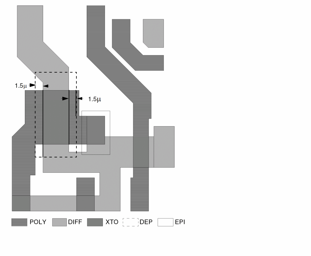
Typical mask design rules for the epi contacts and transistors are as follows:
Minimum epi-contact spacing to a transistor edge
To specify these rules, use the following commands in the Operation block:
*OPERATION
;
; FORM TRANSISTORS OVERSIZED IN SOURCE/DRAIN DIRECTION
;
SIZE poly BY 1 ovpoly ; Oversize polysilicon to expand channels in s/d direction.
AND ovpoly diff ovpodif ; Form ovpodif channels oversized in s/d direction.
NOT ovpodif epi xtor ; Form xtor transistors oversized in s/d direction.
;
; FORM DEPLETION IMPLANT AND ENHANCEMENT BLOCKING
;
OR natural harddep eblk ; Form enhancement blocking layer
OR harddep softdep depl ; Form depletion implant layer
;
ENC[T] xtor eblk LT 2.0 OUTPUT drc02 41 ; Enhancement
ENC[T] xtor depl LT 2.0 OUTPUT drc03 51 ; Depletion
;
EXT[T] eblk xtor LT 2.5 OUTPUT drc02 42 ; Enhancement
EXT[T] depl xtor LT 2.5 OUTPUT drc03 52 ; Depletion
;
EXT[T] epi xtor LT 3.0 OUTPUT drc04 61
;
ENC[T] xtor&pxtor ovpoly LT .001 & ; Or in the direction of diffusion.
EXT[T] &pxtor epi LT 3.0 OUTPUT drc05 62
; diffusion conjunctive rename of xtor layer to &pxtor fs
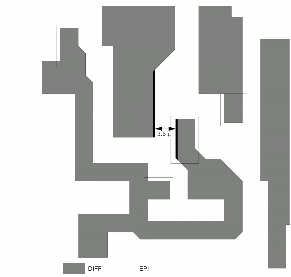
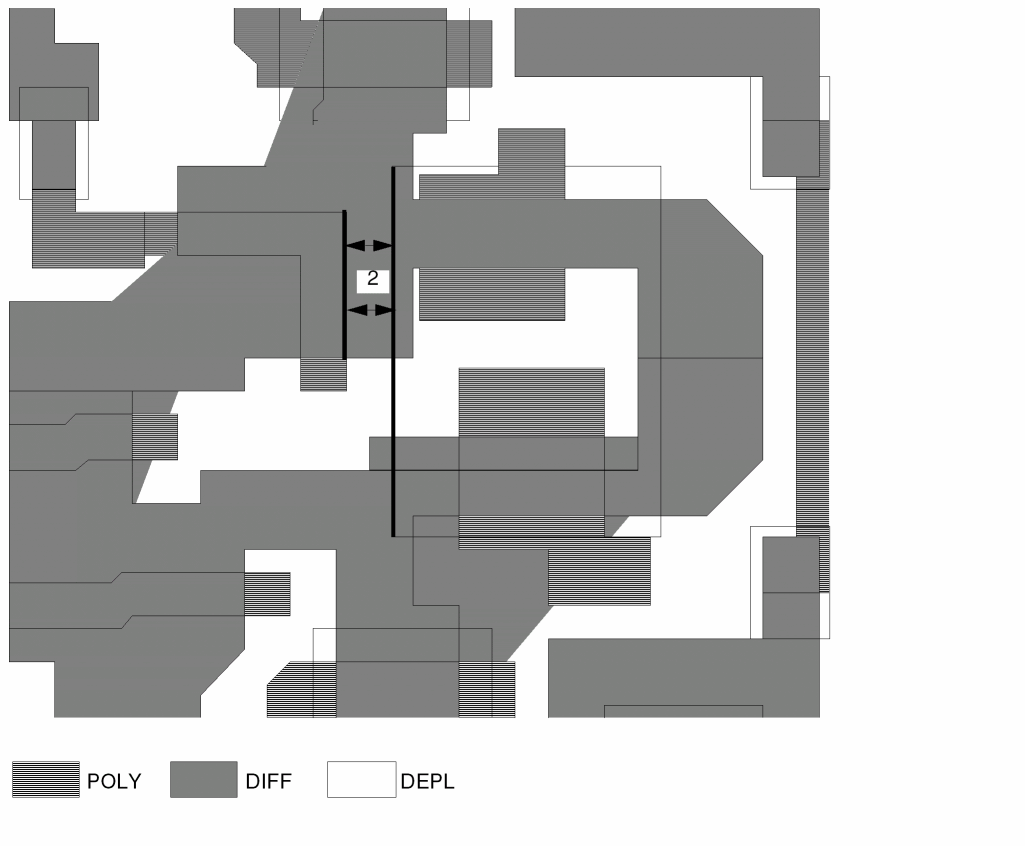
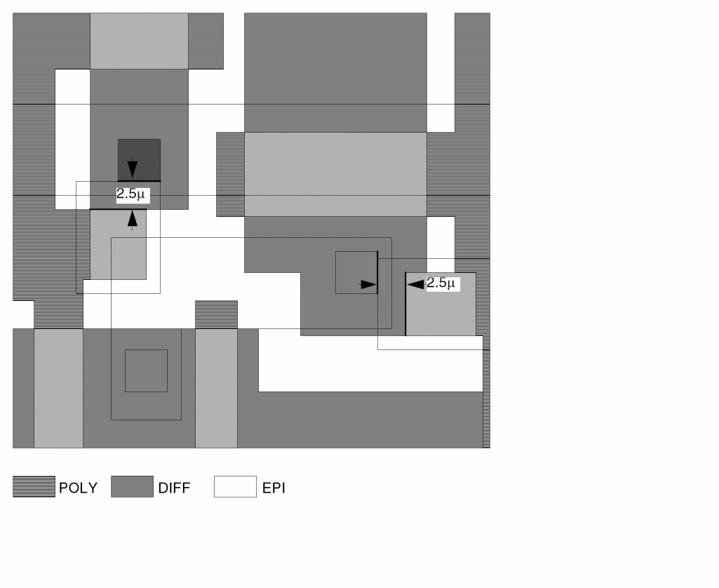
Diffusion Separation Rules
Typical mask design rules for the external separation of the diffusion geometries are as follows:
Minimum diffusion external separation for the diffusion (field) mask when overlapped by an epi contact
Limiting case, no epi overlap 4.0 microns When either of the diffusion lines has an epi contact 4.5 microns When both of the diffusion lines have an epi contact 5.5 microns
To specify these rules, use the following commands in the Operation block:
; Operation block, continued
;
; FORM DIFFUSION EPI-CONTACT OVERLAP LAYER
; diff = Diffusion layer
; epi  = Epi contact layer
;
AND diff epi diffep
;
EXT   diff         LT 4.0  OUTPUT drc01 32
EXT   diff diffep  LT 4.5  OUTPUT drc01 33
EXT   diffep       LT 5.5  OUTPUT drc01 34
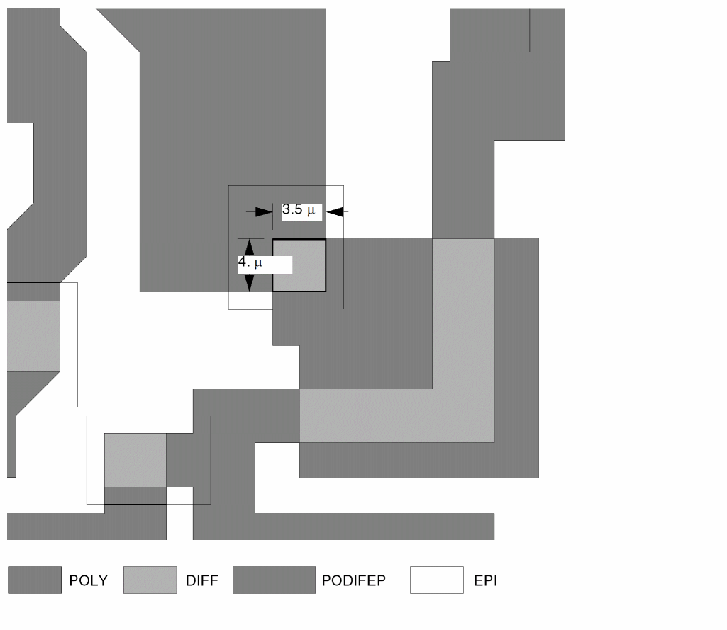
Spacing Rules
This class of design rules includes the minimum spacing required to avoid shorts caused by the IC fabrication process. These rules generally involve external spacing checks between geometries, which tend to produce many false errors unless there is an effective electrical node capability. You can ignore these checks if the geometries are part of the same electrical node, even if the spacing is less than the allowable dimension.
Typical external spacing design rules are as follows:
- Minimum polysilicon-to-diffusion spacing is 1.0 micron (if not in the same electrical node).
- Minimum polysilicon metal contact-to-diffusion spacing is 4.0 microns (if not in the same electrical node).
- Minimum diffusion metal contact-to-polysilicon spacing is 3.5 microns (if not in the same electrical node).
- Minimum diffusion metal contact-to-transistor spacing in the direction of diffusion is 4.0 microns.
To specify these rules, use the following commands in the Operation block:
; Operation block, continued
;
; FORM THE SOURCE-DRAIN LAYER
; poly = Polysilicon layer
; diff = Diffusion layer
; cont = Metal contact layer (mc)
; epi  = Epi contact layer
;
NOT diff poly srcdrn  Form srcdrn = diff - poly
;
; ELECTRICAL NODE DEFINITION
;
CONNECT    metal     poly      BY cont
CONNECT    metal     srcdrn    BY cont
CONNECT    poly      srcdrn    BY epi
;
EXT[N] poly srcdrn LT 1.0 OUTPUT drc05 73
;
; FORM LAYERS OVERLAPPING THE METAL-CONTACTS
;
AND poly   cont mc poly  Form mcpoly polysilicon  metal contact
AND srcdrn cont mc srdn  Form mcsrdn source-drain metal contact
;
EXT[N]     mc poly   srcdrn    LT 4.0  OUTPUT drc06 86
EXT[N]     mc srdn   poly      LT 3.5  OUTPUT drc06 87
;
EXT[T]     &pxtor    mc srdn   LT 3.0  OUTPUT drc06A 87
Enclosure Rules
Sometimes the dimension of the enclosure of a metal contact by the metal layer is larger in the direction of current than in the other direction.
The design rule is the minimum polysilicon-metal contact enclosed by polysilicon enclosure spacing and the minimum metal spacing is 6.0 microns.
To specify this rule, use the following commands in the Operation block:
; Operation block, continued
;
; poly   = Polysilicon layer
; metal  = Metal layer
; cont   = Metal contact layer (mc)
;
ENC[TO]    cont  poly    LT 1.0   OUTPUT drc06 84
;
SIZE      cont BY 3.0 ovmc ; Form metal-entry into metal-contact
AND       ovmc metal  xcmet ; Form metal-direction
ENC[PC]   cont xcmet  RANGE 2.99 3.01 &
ENC[PCTO] cont poly   LT 2.0 OUTPUT drc06 85
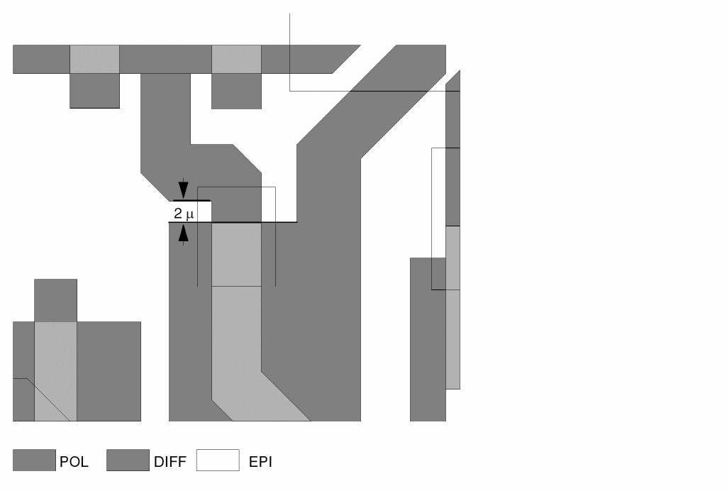
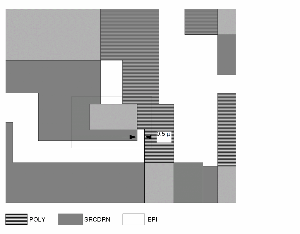
Polysilicon-to-Diffusion Spacing Rules
Most processes require design rules that specify the minimum external spacing between the polysilicon and diffusion geometries. However, when metal crosses adjacent polysilicon and diffusion, the spacing requirement increases. This increase prevents metal from breaking during processing when it runs over the valleys formed by diffusion and polysilicon layers.
Specify the design rule minimum polysilicon-to-diffusion spacing as follows:
To specify this rule, use the following commands in the Operation block:
; Operation block, continued
;
; poly  = Polysilicon layer
; diff  = Diffusion layer
; metal = Metal layer
;
; FORM LAYERS OVERLAPPING THE METAL LAYER
;
EXT[R] poly  diff LT 2.0  valley  ; Form the valley layer
AND  metal  valley  metval  OUTPUT drc05 74
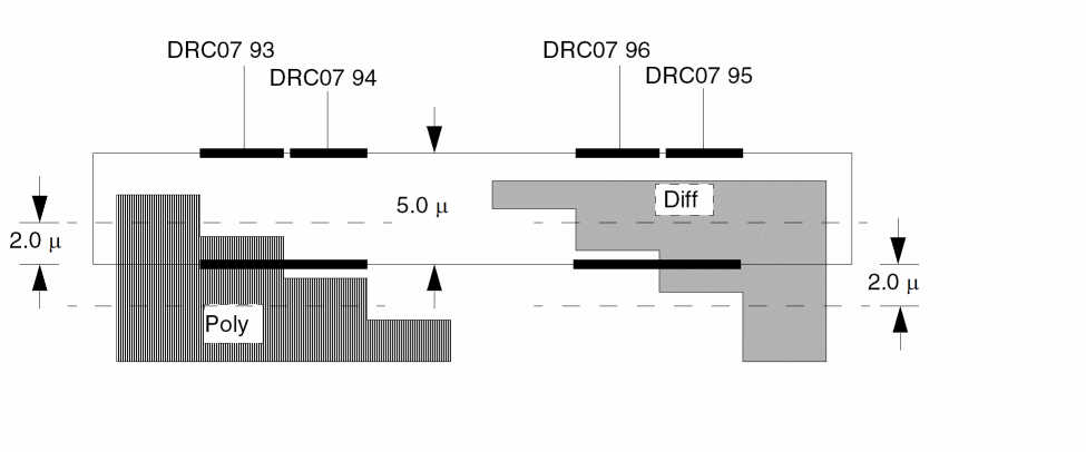
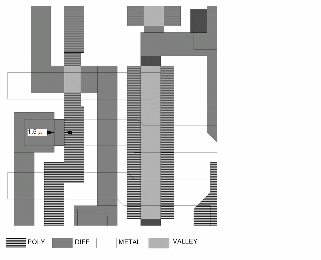
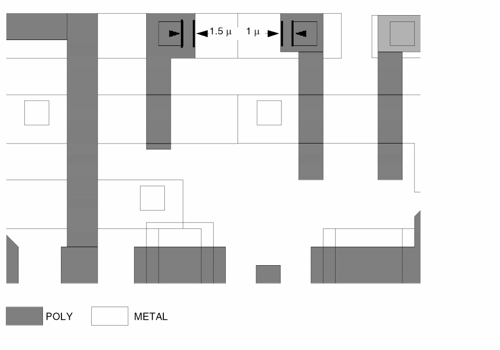
Metal Reflection Rules
The next class of design rules includes checks necessary to prevent adverse effects caused by reflecting light during the IC fabrication process. An adverse effect is often referred to as a “misalignment” or a “hazard.”
As layers of various materials build up during the IC fabrication process, peaks and valleys forming on the IC cause angular light reflection. For example, if shaded areas of the IC mask for the metal layer represent the after-process metal geometries, light might reflect off the deposited metal when light passes through the clear areas in the mask. The following figure, “Cause of Metal Reflection,” shows this lighting effect.
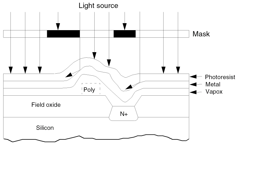
In the following figure, “After-Process Geometries,” the areas under the shaded portion of the IC mask are exposed to light, which results in undersized geometries. The rules used in this example are based on the requirements of a positive photoresist process.
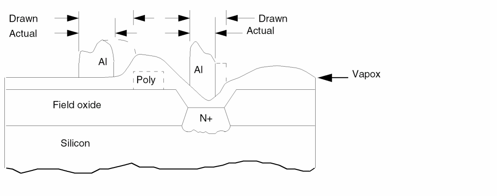
The mask design rules for metal reflection define the minimum width of the metal as follows:
To specify these rules, use the following commands in the Operation block:
; Operation block, continued
;
; poly = Polysilicon layer
; diff = Diffusion layer
; metal = Metal layer
; polymet = Polysilicon and metal layer
;
; LIMITING CASE NO REFLECTION
;
WIDTH     metal   LT 5.0    OUTPUT drc07 92
;
; METAL OVER POLYSILICON REFLECTION CHECK
;
INT[P]    poly    metal     LT 2.0 &
INT[P]    metal   metal[O]  LT 6.0   OUTPUT drc07 93
EXT[TP]   metal   poly      LT 2.0 &
INT[P]    metal   metal[O]  LT 6.0   OUTPUT drc07 94
;
; METAL OVER DIFFUSION REFLECTION CHECK
;
ENC[TP]   metal   diff      LT 2.0 &
INT[P]    metal   metal[O]  LT 6.0   OUTPUT drc07 95
;
ENC[TP]   diff    metal     LT 2.0 &
INT[P]    metal   metal[O]  LT 6.0   OUTPUT drc07 96
Executing DRC from a Design Rule Library
The design rules necessary to comply with the technology in this example are shown in the following Operation block:
*OPERATION
;
; FORM THE SOURCE-DRAIN LAYER
;
NOT         diff        poly            srcdrn
;
; ELECTRICAL NODE CONSTRUCTION
;
CONNECT     metal       poly            BY cont
CONNECT     metal       srcdrn          BY cont
CONNECT     poly        srcdrn          BY epi
;
; LAYER RESIZING OPERATIONS
;
SIZE        poly        BY 1.0          ovpoly
STAMP       ovpoly      BY              poly
SIZE        epi         BY 3.0          ovepi
;
; FORM TRANSISTORS OVERSIZED IN THE SOURCE-DRAIN DIRECTION
;
AND         ovpoly      diff            ovpodif
NOT         ovpodif     epi             xtor
;
; FORM DEPLETION IMPLANT MASK AND ENHANCEMENT BLOCKING MASK ; LAYERS
;
OR          harddep     softdep         depl
OR          natural     harddep         eblk
;
; DESIGN RULE CHECKS
;
; DIFFUSION MASK DRC
;
WIDTH       diff        LT 4.0          OUTPUT drc01 31
EXT         diff        LT 4.0          OUTPUT drc01 32
;
; DIFFUSION WITHIN EPI-CONTACT DRC
;
AND         diff        epi             diffep
;
EXT[P]      diff        diffep          LT 4.5  OUTPUT drc01 33
EXT[P]      diffep      LT 5.5          OUTPUT drc01 34
;
; ENHANCEMENT BLOCKING MASK DRC
;
ENC[T]      xtor        eblk            LT 2.0  OUTPUT drc02 41
EXT[T]      eblk        xtor            LT 2.5  OUTPUT drc02 42
EXT[P]      eblk        LT 3.0          OUTPUT drc02 43
;
; DEPLETION IMPLANT MASK DRC
;
AND         poly        diffep          podifep
;
ENC[T]      xtor        depl            LT 2.0  OUTPUT drc03 51
EXT         depl        xtor            LT 2.5  OUTPUT drc03 52
EXT[P]      depl        LT 3.0          OUTPUT drc03 53
AREA        podifep     RANGE 0.0 20.0  OUTPUT drc03 54
ENC         diffep      epi             LT 1.0  OUTPUT drc03 55
;
; EPI-CONTACT DRC
;
AND         poly        ovepi           ovepipo
AND         srcdrn      ovepi           sdovepi
;
EXT[T]      epi         xtor            LT 3.0  OUTPUT drc04 61
EXT[O]      epi         mc              LE 0.0  OUTPUT drc04 62
EXT[P]      epi         LT 3.0          OUTPUT drc04 63
EXT[N]      ovepipo     sdovepi         LT 3.0  OUTPUT drc04 64
ENC[T]      xtor&pxtor  poly            LT.001 &
EXT[T]      &pxtor      epi             LT 3.0  OUTPUT drc05 62
;
; POLYSILICON MASK DRC
;
WIDTH       poly        LT 3.5          OUTPUT drc05 71
EXT         poly        LT 4.0          OUTPUT drc05 72
EXT[N]      poly        srcdrn          LT 1.0  OUTPUT drc05 73
;
; METAL BREAK
;
EXT[R]      poly        diff            LT 2.0  valley
AND         metal       valley          metval  OUTPUT drc05 74
EXT         metval      LT 2.0          OUTPUT drc05 74
;
ENC         xtor        poly            LT 3.0  OUTPUT drc05 75
;
; METAL-CONTACT DRC
;
AND         poly        cont            mcpoly
AND         srcdrn      cont            mcsrdn
;
AREA        cont        RANGE           0. 9.   OUTPUT drc06 81
ENC         cont        metal           LT 1.0  OUTPUT drc06 82
ENC         cont        diff            LT 2.5  OUTPUT drc06 83
ENC         cont        poly            LT 1.0  OUTPUT drc06 84
SIZE        cont        BY 3.0          ovmc
AND         ovmc        metal           xcmet
ENC[PC]     cont        xcmet           RANGE 2.99 3.01 &
ENC[PCTO]   cont        poly            LT 2.0  OUTPUT drc06 85
WIDTH       xcmet       LT 6.0          OUTPUT drc06 86
EXT[N]      mcpoly      srcdrn          LT 4.0  OUTPUT drc06 87
EXT[N]      mcsrdn      poly            LT 3.5  OUTPUT drc06 88
EXT[T]      &pxtor      mcsrdn          LT 3.0  OUTPUT drc06a 87
EXT         cont        LT 4.0          OUTPUT drc06 89
;
; METAL DRC
;
EXT         metal       LT 4.0          OUTPUT drc07 91
WIDTH       metal       LT 5.0          OUTPUT drc07 92
;
; METAL OVER POLYSILICON REFLECTION
;
INT[P]      poly        metal           LT 2.0 &
INT[P]      metal       metal[O]        LT 6.0  OUTPUT drc0 7 93
EXT[TP]     metal       poly            LT 2.0 &
INT[P]      metal       metal[O]        LT 6.0  OUTPUT drc0 7 94
;
; METAL OVER DIFFUSION REFLECTION DRC
;
ENC[PT]     metal       diff            LT 2.0 &
WIDTH       metal       metal[O]        LT 6.0  OUTPUT drc07 95
ENC[PT]     diff        metal           LT 2.0 &
WIDTH       metal       metal[O]        LT 6.0  OUTPUT drc07 96
;
* END
After you create the Description, Input-Layer, and Operation blocks, you can store the blocks in one or more files. The following examples are files you can use:
Description block drcdesc.com Input-Layer block drcinpl.com Operation block drcoper.com
You can then read the files into the preprocessor using the following PDRACULA commands:
/GET drcdesc NOLIST /GET drcinpl NOLIST /GET drcoper NOLIST /FINISH
Alternatively, you can concatenate these three files into a single file, such as drc.com, and enter the file as follows:
Direct user interface in the Dracula system takes place in the preprocessor, PDRACULA, which is the outermost shell of the verification system. The preprocessor provides execution control and most file management functions.
To start PDRACULA, type the following command:
PDRACULA
The following example shows how to submit a DRC job to PDRACULA. Text you type is shown in bold.
**********************************************************
*/N* DRACULA3 (REV. 4.3 /SUN-4 /GENDATE: 14-AUG-95/07)
*** (Copyright 1995, Cadence) ***
*/N* EXEC TIME =11:35:40 DATE = 16-AUG-95
********************************************************
:/GET drc NO
:/FINISH
**Note: CREATING DEFAULTING CNAMES-CSEN TO "NO" WHEN SYSTEM=APPLICON
**CREATING : COMMAND FILE: jxrun.com
**NOTE: THIS JOB HAS 28 STAGES
END OF DRACULA COMPILATION
Developing and Executing a Design Rule
The preprocessor contains a command language with which you can develop technology processes for future use in production environments. The following example demonstrates the development of the metal-over-polysilicon reflection check. This example is an interactive session with the preprocessor.
Text you type is shown in bold.
To start PDRACULA, type the following:
PDRACULA

:/LIST ALL UNSORTED

*INPUT-LAYER
POLY     =        5
METAL    =        7
*END
*OPERATION
AND      POLY     METAL  POLYMET
WIDTH    POLYMET  LT 2   &
ENC[T]   POLYMET  METAL  LT 0.001  &
WIDTH    METAL    LT 6   OUTPUT    drc07 93
*END

:/STORE yourfile

FILE: YOURFILE EXISTS, OVERWRITE (Y/N) ? Y

:/FINISH

SCALE : .0000152588 MIC (or Rev-Scale = 65536 MIC)
RESOLUTION : .125 MIC
PRIMARY CELL : demo
INPUT-FILE-NAME
(INDISK NAME) : INDISK=demodrc
OUTPUT-FILE-NAME
(OUTDISK NAME) : OUTDISK=demout
SYSTEM : CADENCE
MODE : EXEC NOW

Note:   CREATING PRECHK FILE   :JXPRECHK.COM
        AND RULES FILE         :JXRUN.COM

END OF DRACULA COMPILATION
FORTRAN STOP
Previous logical name assignment replaced
Job 456 entered on queue SYS$BATCH
WITHOUT PRECHECK, THE DRACULA JOB IS SUBMITTED
Viewing the Results
This section contains illustrations of system-generated printed and graphic output of violations. Ten violations are shown. The output cells containing the violations are shown in the examples on the following pages. The violations are the following:
- DRC0132 External Spacing of Diffusion
- DRC0351 XTOR Enclosed by Depletion
- DRC0352 Depletion to Enhanced XTOR in Field Dir
- DRC0354 Minimum Gate Area When within EPI
- DRC0464 Poly to Diffusion Near EPI
- DRC0573 Poly to Diffusion (Node Option)
- DRC0574 Poly to Diffusion When Crossed by Metal
- DRC0685 Metal-Contact between Metal and Poly
- DRC0687 Metal-Contact within Diffusion to Poly
- DRC0792 Width of Metal
Viewing the Summary File
The first step in evaluating a DRC analysis is to scan through the Violation/ Output Cell Summary using an online editor like vi or emacs. The summary contains a definition of the primary cell, cell name, layer number, windowed location in physical units, and number of line-segment violations.
Text you type is shown in bold. To view the file in vi, type the following command at a UNIX command line:
vi Printf.sum
Dracula displays the following information:
* * * * * * * * * * * * * * * * * * * * * * * * * * * * * *
* * * * * * * *         D R A C U L A       * * * * * * * *
* * * * * * * *     *** COPYRIGHT 1995***  * * * * * * * *
* * * * *         RELEASE 4.3 /    1995     * * * * * * * *
* * * * * * * * * * * * * * * * * * * * * * * * * * * * * *
BEGIN AT TIME=12:00:00  DATE=17-AUG-95
CELL  DRC0241  SKIPPED BECAUSE OF NO OUTPUT DATA
CELL  DRC0243  SKIPPED BECAUSE OF NO OUTPUT DATA
CELL  DRC0353  SKIPPED BECAUSE OF NO OUTPUT DATA
CELL  DRC0355  SKIPPED BECAUSE OF NO OUTPUT DATA
CELL  DRC0462  SKIPPED BECAUSE OF NO OUTPUT DATA
CELL  DRC0463  SKIPPED BECAUSE OF NO OUTPUT DATA
CELL  DRC0562  SKIPPED BECAUSE OF NO OUTPUT DATA
CELL  DRC0682  SKIPPED BECAUSE OF NO OUTPUT DATA
CELL  DRC0684  SKIPPED BECAUSE OF NO OUTPUT DATA
CELL  DRC0686  SKIPPED BECAUSE OF NO OUTPUT DATA
CELL  DRC0688  SKIPPED BECAUSE OF NO OUTPUT DATA
CELL  DRC0796  SKIPPED BECAUSE OF NO OUTPUT DATA
-------------- OUTPUT CELL SUMMARY ----------------
CELL      LAYER  # OF POLYGON
NAME      #      W I N D O W  LINE SEGMENTS
DRC0131   31     17.000       25.500   282.500  233.500  70
DRC0132   32     90.500       40.500   112.500  172.000  10
DRC0133   33     30.000       20.000   275.500  242.000  42
DRC0134   34     111.000      15.500   124.500  156.500  24
DRC0242   42     123.000      184.500  125.000  208.500  4
DRC0351   51     41.000       156.500  42.500   174.500  2
DRC0352   52     123.000      184.500  125.000  208.500  4
DRC0354   54     98.000       29.000   351.500  169.500  3
DRC0461   61     30.000       92.000   31.625   95.500   2
DRC0464   64     29.500       19.500   275.500  161.500  34
DRC0571   71     302.000      .000     350.000  262.000  6
DRC0572   72     41.000       7.000    286.000  257.000  24
DRC0573   73     261.000      35.500   266.500  226.500  20
DRC0574   74     9.000        15.000   150.500  247.000  28
DRC0575   75     30.000       90.625   36.000   94.125   4
DRC0681   81     86.500       .000     348.500  262.000  14
RC0683    83     36.000       16.000   288.000  265.000  14
DRC0685   85     369.000      6.000    370.000  256.000  8
DRC0687   87     41.000       44.500   321.500  257.000  10
DRC0791   91     142.000      .000     411.000  265.000  10
DRC0792   92     69.000       .000     395.000  262.000  14
DRC0793   93     364.000      128.500  393.500  133.500  4
DRC0794   94     75.000       79.000   267.375  221.000  6
DRC0795   95     12.000       152.500  18.000   160.000  4
PRIMARY CELL= OUTDEMO
WINDOW    =      9.000        .000     411.000  265.000
********* PROBLEM GEOMETRIES LISTING *********
CELL: MB297 LAYER: 2 PROBLEM GEOMETRIES:ACUTE  -PROCESSED
-1123.00 233.00 -1123.00 187.00 -1254.00 187.00 -1254.00 202.00
-1275.00 202.00 -1275.00 187.00 -1384.00 187.00 -1384.00 233.00
-1373.00 233.00 -1373.00 227.00 -1293.00 227.00 -1293.00 233.00
-1248.00 233.00 -1248.00 227.00 -1168.00 227.00 -1168.00 233.00
-1168.00 228.00 -1168.00 233.00 -1123.00 233.00
CELL: BLK1 LAYER: 9  PROBLEM GEOMETRIES:OPEN POLYGON -DISCARDED
- 380.00 282.00 -379.90  282.00 -1337.00 299.00 -1127.90 399.00
-1108.90 380.00
***** END OF PROBLEM GEOMETRIES LISTING *****
Viewing the Log Files
To print a detailed listing of the design rule violations in the .log and .drc files, use the LISTERROR command in the Description block.
The listing of design rule violations shown below lists the type of checks performed, names of the layers, value of the checks, output layer numbers, and output cell names. For each violation, the x,y coordinates of the two line segments are printed in physical units.
EXTERNAL CHECK - DIFF SPACING = 4.000 ( 32.0 DBU)
OUTPUT LAYER # = 32 OUTPUT CELL NAME = DRC0132
ERR --- LAYER DIFF --- --- LAYER DIFF ---
  #  X1      Y1      X2      Y2      X1      Y1      X2      Y2

  1  90.500  40.500  90.500  43.500  94.000  44.000  94.000  44.500
  2  90.500  40.500  90.500  43.500  94.000  44.500  94.000  56.500
  3  90.500  87.500  90.500  90.500  94.000  74.500  94.000  86.500
  4  90.500  87.500  90.500  90.500  94.000  86.500  94.000  87.000
  5 109.000 160.000 109.000 172.000 112.500 157.500 112.500 162.000
Viewing the Violations
The examples on the following pages show the graphic output for the violations previously defined. Each page shows an example of a layout violation and the commands that flagged the violation.
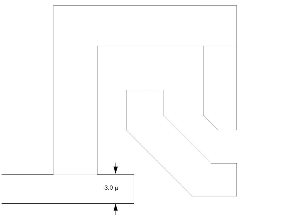
DRC0132 External Spacing of Diffusion
EXT diff LT 4.0 OUTPUT drc01 32
DRC0351 XTOR Enclosed by Depletion
ENC[T] xtor depl LT 3.0 OUTPUT drc03 51
DRC0352 Depletion to Enhanced XTOR in Field Dir
EXT diff xtor LT 2.5 OUTPUT drc03 52
AREA podifep RANGE 0 20 OUTPUT drc03 54
EXT[N] ovepipo sdovepi LT 3.0 OUTPUT drc04 64
EXT[N] poly srcdrn LT 1.0 OUTPUT drc05 73
DRC0574 Poly to Diffusion When Crossed by Metal
EXT[R]   poly   diff    LT 2.0  valley
AND      metal  valley  metval  OUTPUT drc05 74
DRC0685 Metal-Contact Between Metal and Poly
SIZE        cont  by 3.0  ovmc
AND         ovmc  metal   xcmet
ENC[PC]     cont  xcmet   RANGE 2.9 3.1 &
ENC[PCTO]   cont  poly    LT 2.0  OUTPUT drc06 85
DRC0687 Metal-Contact Within Diffusion to Poly
EXT[N] mcsdrn poly LT 3.5 OUTPUT drc06 87
DRC0792 Width of Metal
WIDTH metal LT 5.0 OUTPUT drc07 92
Database Comparison
The following rules file demonstrates a DRC check that compares digitized layers of one database to layers of another database. The output is in a graphic format.
To submit the comparison job, type the following:
% PDRACULA
:/GET compare1.com n
:/NEXT
:/GET compare2.com n
:/FIN
This database comparison first runs the compare1.com job to read in the first database layers. Then the database comparison runs the compare2.com job to read in the second database layers and perform the graphic comparison. The summary report file is comprt.sum, and the graphic output file is comout.dat.
Hierarchical and Multilevel Hierarchical Design Rules Checker
HDRC provides the design rule checking function for hierarchical Dracula. Before reading this section, you should be familiar with the information about hierarchical Dracula found in the Introducing Dracula section in chapter 1 of this manual.
As chip complexity and device count increase, the need for CPU time and disk space also increases. Dracula supports two-level hierarchical design rule checking (HDRC) and multilevel (MDRC) checking. MDRC supports multilevel design hierarchy so you can reduce the verification time and disk storage. Dracula has the following check modes: flat, cell, composite, hierarchical, and multilevel.
The following information is described in this section:
- Hcell selection
- Hcell creation, Hcell environments, and the composite plane
- HDRC modes
- HDRC error reports
- Sample HDRC rules file
For more information about running HDRC, see “
Prerequisites
You need the following data to run HDRC:
- An HDRC rules file
-
A database file in one of the database formats that Dracula supports
For a list of the supported database formats, refer to the SYSTEM or SYSIN section in Chapter 11 of this manual.
Selecting HDRC Hcells
In both hierarchical and cell modes, HDRC automatically selects Hcells according to internal criteria. This automatic selection of Hcells applies only to HDRC. The selection process initially assumes that all cells in the layout are Hcell candidates, except for those you declare in NOT-HCELL commands. Dracula applies each of the criteria in the following table, “Criteria for HDRC Hcell Selection,” to the Hcell candidates, successively eliminating candidates from the group. Dracula uses only cells that meet all five criteria.
In addition, you can select Hcells by using the HCELL and HCELL-FILE commands. Or, in hierarchical mode only, you can exclude Hcells with the NOT-HCELL command. These commands override the default selection. However, these commands can affect the selection of other Hcells.
In hierarchical mode only, you can modify the automatic Hcell selection process by changing the parameters with the HCELL-RULE command. If you do not know the layout hierarchy, run the default Hcell selection first. Then use the HCELL-RULE command to set your own parameters. You can also use the RAM-CELL and ROM-CELL commands to improve the run performance when RAM and ROM cells are present.
To turn off automatic cell selection, specify an HCELL-RULE command with parameters that prevent the automatic selection of Hcells. For example, N = 9999 and M = 9999. In this case, the HCELL command determines which Hcells to use. The following table shows the N and M parameters.
Creating Hcells, Hcell Environment, and Composite Plane
To perform HDRC, the Dracula program first builds the Hcells, Hcell environments, and composite plane data structures.
After Dracula defines an Hcell, the program generates a horizontally aligned rectangular box large enough to encompass all the flattened geometries in that Hcell. Dracula then outputs the Hcell box created to the CELLBOXX layer for later reference. You can access this data through the CELLBOXX.DAT file.
Hierarchical mode HDRC uses the Hcell environment. This environment can be thought of as a box that encompasses the Hcell and extends beyond it. Any geometries (from the composite level or from another Hcell) within an Hcell environment are considered part of that instance of the Hcell (refer to the following figure, “Building the Hcell Box and Hcell Environment”). By default, the Dracula program sets the environment equal to the largest spacing value specified in any spacing check. However, if you use the ENVIRONMENT-MAX command and the preprocessor detects a spacing value greater than the ENVIRONMENT-MAX value, it warns you of the error.
If any DRC rule specifies the S option, the value affects the environment calculation. By default, the environment value is
max(drc rules)
If any DRC rule specifies the S option, the environment value is
max(drc rules, sqrt(2)*(drc rule with S option)
If you have already set the ENVIRONMENT-MAX value, the value specified with the S option overrides the final environment value.
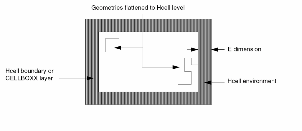
The Hcell plane is the collection of Hcells and their environment information. You can refer to individual layers or all layers in the Hcell plane. The composite plane contains all geometries not included in any Hcell boxes.
Dracula uses composite plane data and Hcell environment data in hierarchical mode only.
HDRC Modes
HDRC runs in five modes: flat, cell, composite, hierarchical, and multilevel.
Flat Mode
Flat mode HDRC processes input data and output error cells in the same manner as flat Dracula. Dracula expands layers and does not retain hierarchical information for error reporting. However, HDRC attempts to group like commands together to reduce overhead time in loading layers, and as a consequence can have faster run times.
Flat mode is the default mode.
Cell Mode
Cell mode HDRC verifies only cells that qualify as Hcells, not nonHcells or the interconnects between Hcells. This mode generates Hcell-based output, with a single output error cell for each Hcell. These error cells contain all the errors associated with that Hcell and any pseudo-layers created and output by a LOGICAL, SIZE, or SELECT operation. You need to separate different error flags with unique output layer numbers, so Dracula can isolate the error flags in the Hcell output.
To run a job in cell mode, use the CHECK-MODE=cell command in the Description block.
Composite Mode
Composite mode HDRC checks the interconnections between Hcells, and between Hcells and composite-level cells. Dracula treats Hcells as “black boxes” and does not check inside Hcells.
To run a job in composite mode, you use the CHECK-MODE=composite command in the Description block.
Hierarchical Mode
Hierarchical mode HDRC completely verifies the circuit and outputs the results in hierarchical form. All cells and interconnects are checked. This mode is best for circuits containing a high degree of hierarchy. This mode can also generate Hcell-based output, with a single output error cell for each Hcell.
To run a job in hierarchical mode, you must use the CHECK-MODE=hier command.
The following limitations apply to hierarchical mode HDRC checks:
CONNECT STAMP LINK SELECT with LABEL SELECT[N] EXT[N] ENC[N] INT[N]
These commands check hierarchical layers when you use the EXCEPTION-ON=AUTO-FLATTEN command in the Description block of your rule file or if you first flatten the layers with the FLATTEN command. The AUTO-FLATTEN option automatically flattens all layers you use in a CONNECT command.
Dimensional-Spacing Checks
Do not use values larger than 10 microns in dimensional checks, such as ENCLOSURE, EXTERNAL, WIDTH, INTERSECT, and LENGTH commands. Large values slow down the checking. If you want a few large dimensional checks, code these checks differently to avoid performing large dimensional checks on hierarchical layers. For example, consider the following checks:
EXT pad LT 50 OUTPUT err1 1
EXT pad metal LT 40 OUTPUT err2 33
You can rewrite the commands as shown in the following examples.
FLATTEN  pad fpad ;  FPAD is a flat layer
EXTERNAL fpad  LT 50 OUTPUT err1 1
FLATTEN   metal  fmet1   ; FMET1 is a flat layer
EXTERNAL  fpad   fmet1   LT 40 OUTPUT err2 22
The FLATTEN metal fmet1 command can use a great deal of CPU time because the metal layer can be very large or dense. A better approach is to take advantage of hierarchical commands and of the pad layer, which is sparsely populated, as shown in the following example:
SIZE pad  BY  40  spad     ; this is a hierarchical
                           ; SIZE and very little cpu
                           ; time is required because
                           ; PAD is a low density layer.
AND spad  metal   smet     ; SMET is a hierarchical
                           ; layer and only has data
                           ; around the PADs.
FLATTEN   smet    fmet2    ; FMET2 is a flat layer
EXTERNAL fpad fmet2  LT 40 OUTPUT err3 33
When doing external spacing checks, the resolution value must be at least one-half your minimum DRC value. For example, if you have a DRC spacing value of 5.25, the resolution must be .125.
Multilevel Mode
Multilevel hierarchical DRC (MDRC) is different from full hierarchical DRC in that not every cell in your design hierarchy is used as a verification Hcell. Dracula chooses only a subset of cells to be Hcells. The major difference between Dracula hierarchical mode and Dracula multilevel mode is that an Hcell in multimode can contain another Hcell.
MDRC consists of two phases: the pre-analysis phase and the analysis phase. The pre-analysis phase selects suitable Hcells by thoroughly analyzing your design data. The output of the pre-analysis phase is the MULTICEL.TAB file, which contains the selected Hcells. Each Hcell in the file is a checking cell. To run a job in multilevel mode, use the CHECK-MODE=multi command in the Description block.
For more information on using MDRC, see “
Rule Check
Multilevel DRC Example
-
Create the jxrun.com file using the following command:
/GET drc.rul MULTI
The contents of drc.rul appear on the screen and Dracula creates the two-stage jxrun.com file used to perform data analysis and multilevel Hcell selection. -
Execute jxrun.com.
Dracula writes the selected multilevel Hcells to the MULTICEL.TAB file. -
Rerun PDRACULA using the following command:
/GET drc.rul N
PDRACULA does the following: -
After PDRACULA completes, execute jxmult.com.
Dracula executes the jxrun.com files in each subdirectory consecutively.
Hcell Selection
PDRACULA uses the following criteria to select cells for Hcells:
-
Cells must exceed the requirements specified in the HCELL-RULE command.
The default number of placements is four. The default number of segments is 1,024 times the number of layers. - If both parent and child qualify as Hcells, PDRACULA checks if the total number of line segments (after expansion) of the child exceeds 90 percent of that of the parent. If so, Dracula selects only the child cell as an Hcell.
- Cells must not violate overlap criteria set by the CHECK-MODE command.
- Dracula writes multilevel cells with over 100,000 line segments to the MULTICEL.TAB file.
HDRC Error Reports
HDRC error reports include the following:
HDRC commands that have an output specification create an error cell similar to flat Dracula if error segments are generated in the composite plane or in flat mode. When run in hierarchical mode, these commands output Hcell error segments to a new or existing Hcell error cell. Hcell error cells can store error segments hierarchically. Dracula stores Hcell-related error segments in either error cell depending upon the uniqueness of the violation. The “HDRC Output Error Format” section in this chapter has more details on the various types of error cells.
Error cells and Hcell error cells have the same polygon format as the input database (GDS II) unless you explicitly specify a different output format with the SYSOUT command. This means you can take these error cells back to the original graphics system, overlay them on the original layout, and see the location of the design rule violations.
The Error Summary file (PRINTF.SUM) contains a summary of the composite plane and Hcell plane error segments. This file is described in the “HDRC Error Summary File” section in this chapter.
HDRC Output Error Format
Dracula sends output error segments from HDRC/DRC spacing checks to an output error file on disk. The OUTDISK command in the Description block determines the name of the output file. The output error file contains a primary output cell that points to the various error cells created. Dracula stores these error cells in files in your host system.
Dracula can store HDRC error segments in two different types of error cells: composite error cells and Hcell error cells.
The following factors determine what kind of error cells contain the error segments:
- The mode, whether flat, cell, composite, hierarchical, or multilevel
- The selected CELL-ERROR-REP option
- The location of the error
Hcell Errors
You select the CELL-ERROR-REP option when you run an HDRC in hierarchical mode. These options establish what to do with errors associated with all instances of an Hcell or all instances of an Hcell environment. The following options are available:
Displays Hcell error segments in the composite plane at the first Hcell placement starting from the bottom left of the layout. This is the default.
Places the Hcell error segments at all instances in the composite, as would be done in a flat mode DRC.
Displays Hcell error segments in a hierarchical manner at all placements in the composite. Outputs error segments to one of the following error cells according to the rules described in the following sections.
Reports error cells and output cells generated by the layer operations (for example, SIZE and SELECT operations) in the original design hierarchy.
Reports DRC error flags in the original cell.
Reports error flags only from the cell name you specify for the output error cell.
Composite Error Cell
Dracula uses this type of error cell for error segments generated in flat mode, which is the same as in flat Dracula. For hierarchical mode, the cell receives error segments when any of the following conditions occur:
- The error segment is in the composite plane
- CELL-ERROR-REP = ONCE or ALL
- CELL-ERROR-REP = HIER and the error segment is not common for all placements of the Hcell or Hcell environment
Hcell Error Cell
The Hcell error cell receives error segments for cell mode and hierarchical mode when CELL-ERROR-REP=HIER and Dracula finds error segments within an Hcell or its environment for all placements of the Hcell.
Duplicate error segments in error cell types can occur in the following cases:
- An error segment occurring only in the environment of an Hcell for all placements of that Hcell appears both in a composite error cell and an Hcell error cell
- An error segment in an area overlapped by two cells for all placements of the two cells appears in both Hcell error cells
The output error file is organized by an output primary error cell (OUTname) containing the two types of error cells. For naming conventions for the output primary cell, see the OUTLIB section in Chapter 11 of this manual. The following example details the organization of the output primary cell.
Primary Error Cell Names
Composite error cells generated for:
| Error-Cell-2 | |
| ... | |
| Error-Cell-n1 |
Hcell error cells generated for:
Each error cell receives its data from the output of a different HDRC spacing check command. For example:
WIDTH METAL LT 5 OUTPUT ERR2 56
generates error segments destined to a composite error cell (ERR256). Dracula creates this error cell and stores the segments in layer 56.
Error Cell File Names
The first part of error cell file names is obtained by concatenating the spacing check command error cell name (c-name) and the layer number (l-num). In the example above, the error cell name is ERR256.
The concatenation of the error cell name and layer number specified in the spacing check command must be unique, the same as in flat Dracula. The layer number, however, can be the same for the various commands.
Dracula puts error segments in error cells relative to the 0,0 coordinates of the primary cell in the original database. Therefore, if you overlay the error cells on your original database, whether you place one cell at a time or all cells together, you must place them at coordinates 0,0.
Hcell error cells can contain error segments from more than one HDRC spacing check, but only from error segments associated with one Hcell. Because HDRC spacing checks are output on different layers, each Hcell error cell can contain many layers. For example:
WIDTH METAL LT 5 OUTPUT ERR1 56
WIDTH POLY LT 5 OUTPUT ERR2 57
WIDTH MC LT 5 OUTPUT ERR3 58
All three commands generate error segments for an Hcell named abc and an Hcell named bcd. Dracula generates error segments for an Hcell error cell corresponding to abc and bcd under the three different layers (56, 57 and 58). Each layer contains the error segments generated by each of the corresponding WIDTH commands. No error cell structure exists for cells. You must separate errors by layer number.
Dracula creates an Hcell error cell file for cell ABC and names it ABC_CEL for GDS II or ABC_CEL;1 for Applicon. Dracula adds _CEL to the GDS II Hcell error cell name to avoid a cell name conflict with abc from your database.
HDRC Error Summary File
The first item in the Error Summary file (PRINTF.SUM) shows the type of error reporting you requested in the CELL-ERROR-REP command.
The “All Error Cells” section lists all output error cells specified in an HDRC or DRC spacing check command, whether or not Dracula creates any error cells.
The “Output Cell Summary” section of the error summary file has entries containing the following items:
- Error cell names and corresponding layer numbers generated by HDRC/DRC spacing checks that generate error segments to be sent to the composite plane
- The minimum and maximum X and Y composite plane coordinates of the smallest window containing the error segments
- The number of error segments output to the error cell. In flat mode, Dracula sends all error segments to error cells. While in hierarchical mode, Dracula outputs some error segments to error cells and some to Hcell error cells, as explained in the “HRDC Output Error Format” section.
The “Detailed Summary for Cell and Cell-Comp Errors” section (provided for hierarchical mode HDRC runs) summarizes the error segments related to Hcells. (See the Example of HDRC Error Summary for Hierarchical Mode in this chapter). These error segments are either fully enclosed by an Hcell, or are located in the Hcell environment, while having a complementary error segment within the Hcell. Dracula reports two categories of errors:
-
Hcell Errors
Errors associated with all placements of an Hcell. Typically, these are errors fully contained in the Hcell. -
Cell-Comp Errors
Errors associated with only some placements of an Hcell. The name “Cell-Comp error” reflects that these error segments are always output on the composite plane (see the Hcell Error Cell section in this chapter). These errors are typically found between cell geometries and their environments.
The report divides the errors along two dimensions. The columns reflect the subset of the errors for the various Hcells. The rows reflect the subset of the errors according to the error cells you specified in the OUTPUT option of the HDRC/DRC spacing check commands.
Dracula labels the columns with the file name of the Hcell. Dracula labels the rows with the file name of the error cell or with the label Cell-Comp under the error cell file name.
A number at the intersection of an Hcell and an error cell name reflects the number of Hcell error segments that Dracula outputs to this error cell. For this case, Dracula counts each error segment only once, independent of the number of placements of the Hcell.
If the number in a row is labeled “Cell-Comp,” Dracula indicates the number of Cell-Comp error segments associated with the Hcell column and the error cell named in the preceding row. Dracula counts this number as one error per placement.
Example of HDRC Error Summary for Hierarchical Mode
The report has two column totals, one for the Hcell errors and another for Cell-Comp errors. The report also has row totals.
The summary report ends with the primary error cell name, as well as the x, y coordinates of the smallest window that includes all the errors found. The summary ends with the time and date the run ended.
*********************************************************/
*/N* DRACULA3 (REV. 4.3 /SUN-4 /GENDATE: 16-AUG-95/07)
 *** (Copyright 1995, Cadence) ***
*/N* EXEC TIME =12:21:30 DATE = 18-AUG-95
********************************************************
------------------ ALL ERROR CELLS LISTING ----------------
D529829    D5610B32  PPCPW28   D5314A30  D5314B30
D52729     D531330   BAD1FF28  D524A29   D523A29
D52629     D57133    D52229    D523B29   D524B29
D52529     D52829    D531A30   D531B30   D532A30
D532A230   D53330    D534A30   D535A30   D536A30
D536B30    D536C30   D53930    D55131    D55231
D55331     D55431    D55531    D56132    D561B32
D56232     D56332    D561132   D56732    D56432
D561232    D56832    D569A32   D569B32   D5610A32
D57233     D573A33   D57433    D57533    D576A33
D576833    D58234    D58334    D58434    D58534
D59135     D928D35   D593A35   D593B35   D596A35
D596B35    D599A35   D510135   D510235   D5103A35
D5103B35   D5103C35  D5103D35  D510535   D510735
D510835    D5131A36  D5131B36  D5132A36  D5132B35
D5132C36   D5133A36  D513336   D5133B36  D133C136
D133C236   D5134A36  D5134B36  D5134C36  D513536
D5136A36   D5136B36  D513836   D5139A36  D5139B36
D1310A36   D1310B36  D5131136  D1312A36  D1312B36
D131436    D515137   D515237   D515337   D5133C37
D514437
BEGIN AT TIME = 06:11:51 DATE = 16-AUG-95
-------------------- OUTPUT CELL SUMMARY ----------------------
CELL-NAME LAYER #   -------- WINDOW --------
          DATATYPE                        # OF POLYGONS TEXTS
                                          (LINE SEGMENTS)
D5314B30   30  -703.500   -1015.500  865.000   752.00    2
D57133     33  -651,000   -1165,000  830.500   -978.50   34
D523B29    29  -1301.500  -1293.000  1049.500  1143.00   538
D534A30    30  -938.500   -1309.500  1310.000  907.50    238
D535A30    30  -1037.500  -1309.550  1310.050  917.00    280
D536A30    30  -1179.000  -1258.500  1211.000  1286.50   2518
D536C30    30  -651.000   -1161.400  830.500   -981.50   68
D561B32    32  -680.600   -926.050   882.300   719.00    26612
D56732     32  -871.900   -1162.500  886.000   725.00    170416
D57433     33  -653.000   -1166.000  832.500   -977.00   533
D58234     34  -659.500   -1161.500  839.000   -981.50   66
D599A35    35  -445.500   -1141.000  21.000    -1049.004
D5103A35   35  -652.500   -1168.500  888.500   722.50    304
D510835    35  -333.500   -1181.500  799.000   -1129.50  10
D5131A36   36  -664.800   -923.500   848.800   -922.50   672
D5131B36   36  -869.500   -885.500   -846.000  -884.00   2
D5133A36   36  864.000    -943.500   880.000   -936.50   8
D1310A36   36  -643.000   -1168.500  822.500   -975.00   100
D1310B36   36  -652.500   -1168.500  832.000   -975.00   68
D1312A36   36  -643.000   -1165.000  822.500   -978.50   106
OUTDISK OPTION IS:
EXPLODE CELL GEOMETRIES INTO PRIMARY CELL FOR ALL PLACEMENTS (CELL-ERROR-REP = ALL)
--- DETAILED SUMMARY FOR CELL AND CELL-COMP ERRORS
(NO. OF POLYGONS) ---
NOTE: THE FOLLOWING POLYGON COUNTS DO NOT INCLUDE ERRORS CAUSED ONLY BY COMPOSITE GEOMETRIES
           H   T   A   A   A   A   A   A   A   A   A   A   A
           C   O   D   D   D   D   D   D   D   D   D   D   D
           E   T   0   5   0   0   0   2   6   7   7   7   7
           L   A   5   0   1   2   7   0   0   0   0   0   0
           L   L   .   1   .   .   .   1   2   2   5   3   4
           S       C   .   C   C   C   .   .   .   .   .   .
                   E   C   E   E   E   C   C   C   C   C   C
                   L   E   L   L   L   E   E   E   E   E   E
                   ;   L   ;   ;   ;   L   L   L   L   L   L
                   0   ;   0   0   0   ;       ;   ;   ;   ;
                       0               0   0   0   0   0   0
ERRCELL
D523B29    CEL:  36   2    14   0   0  6  2  12   0   0   0   0

CELL-COMP:       4    0    0    0   4  0  0  0    0   0   0
D535A30    CEL:  3    0    0    0   0  3  0  0    0   0   0   0
D536A30    CEL:  68   0    26   6   6  4  0  26   0   0   0   0
D536C30    CEL:  4    0    0    0   0  0  0  0    4   0   0   0
D561B32    CEL:  108  0    0    0   0  0  0  0    48  12  24  12
D56732     CEL:  406  0    0 0  0   0  0  0  119  88  39  80
CELL-COMP:       6    0    0    0   0  6  0  0    0   0   0   0
D57433     CEL:  32   0    0    0   0  0  0  0    32  0   0   0
D58234     CEL:  4    0    0 0  0   0  0  0  4    0   0 0
D5103A35   CEL:  18   0    0    0   0  0  0  0    12  6   0   0
D5131A36   CEL:  14   0    0    0   0  0  0  0    14  0   0   0
CELL-COMP: 448   0    0    0    0   0  0  0  0    0   0   0
D5131B36   CEL:  0
CELL-COMP:       1    0    0    0   0  1  0  0    0   0   0   0
D1310A36   CEL:  6    0    0    0   0  0  0  0    6   0   0   0
D1310B36   CEL:  4    0    0    0   0  0  0  0    4   0   0   0
D1312A36   CEL:  6    0    0    0   0  0  0  0    6   0   0   0
---------------
TOTAL
CELL:        709  2  40  6  6  13  2  38  249  106  63  92
CELL-COMP:   459  0  0   0  0  11  0  0   0    0    0   0
PRIMARY CELL:   OUTAD000
WINDOW:     -1301.500     -1309.550     1310.050     1286.500
ENDED  AT  TIME  = 06:12:25     DATE = 16-AUG-95
HDRC Error Summary for Cell Mode
In cell mode, an HDRC run produces a different summary report (PRINTF.SUM) than in hierarchical and flat modes. The summary is divided into two sections and summarizes the number of error segments found by the HDRC checking commands for each Hcell.
The “All Error Cells Listing” section contains the name of all the Hcells used and the time and date the run started.
The “Individual Cell Summary” section contains information about the number of error segments generated for every error cell output specification under each Hcell. Each entry has a line with an Hcell name, followed by one or more lines with an error cell name, a corresponding layer number, data type, and total number of error segments under this Hcell and this error cell. A final line shows the total number of error segments for error cells under this Hcell and the X, Y coordinates of the smallest window in the Hcell that contains all the errors. These window coordinates are relative to the coordinates of the Hcell in the original database.
Example of HDRC Error Summary for Cell Mode
-----------------------ALL ERROR CELLS LISTING-------------
DD01     DD02
        BEGIN  AT  TIME = 12:20:23             DATE = 16-AUG-95
----------------- INDIVIDUAL CELL SUMMARY------------------
CELL NAME: SDFF4_CEL
ERROR-CELL: DD02 LAYER/DATATYPE: 2/ 0 # OF POLYGONS:22
WINDOW: -7.000 9.000 220.000 121.000 TOTAL POLYGONS:22
CELL NAME: SB1_CEL
ERROR-CELL: DD02 LAYER/DATATYPE: 2/ 0 # OF POLYGONS: 1
WINDOW: -6.000 -11.000 66.500 11.000 TOTAL POLYGONS: 1
CELL NAME: ROM_CEL
ERROR-CELL: DD02 LAYER/DATATYPE: 2/ 0 # OF POLYGONS: 6
WINDOW: -7.000 -7.000 105.000 51.500 TOTAL POLYGONS: 6
CELL NAME: SB2_CEL
ERROR-CELL: DD02 LAYER/DATATYPE: 2/ 0 # OF POLYGONS: 1
WINDOW: -6.000 -11.000 66.500 11.000 TOTAL POLYGONS: 1
CELL NAME: SDFF1_CEL
ERROR-CELL: DD02 LAYER/DATATYPE: 2/ 0 # OF POLYGONS: 57
WINDOW: -9.000 -17.000 250.000 206.500 TOTAL POLYGONS: 57
PRIMARY CELL: OUTDEMO
WINDOW: -9.000 -17.000 250.000 206.500
Sample HDRC Rules File
*DESCRIPTION
CHECK-MODE = hier
ENVIRONMENT-MAX = 7 mic
 ;
MODE      = exec no
SCALE     =.001 mic
RESOLUTION= .25 mic
PRINTFILE = hdrc
PROGRAM = drac3:
SYSTEM = gds2
PRIMARY = demo
INDISK  = demo.db
OUTDISK = hdrcout
*END
*INPUT-LAYER
diff  =  1
epi   =  7
poly  =  4
metal =  6
pad  =  17
PIN-TEXT-LAYER = pinlay
CONNECT-LAYER = fpol fsd  ; PREPARE FOR NODAL CHECK IN HDRC
*END
*
AND       poly    diff     gate
NOT       diff    gate     srcdrn
WIDTH     diff    LT 5     OUT      w5001  30 3
EXT[H]    diff    LT 5.5   OUT      x5002  31 4
WIDTH     poly    LT 4.5   OUT      w5003  32
EXT       poly    LT 4.0   OUT      x5004  33
EXT       poly    srcdrn   LT 2.0   OUT    x5013  41
EXT[T]    poly    diff     LT .001  OUT    x5013  42
WIDTH     srcdrn  LT 5.5   OUT      w5013  42
WIDTH     gate    LT 5.0   OUT      w5016  45
WIDTH     epi     LT 7.0   OUT      w5020  52  4
ENC[T]    diff    poly     LT 4.0   OUT    e5301  57  7
;****  NEW  *****          ; PREPARE FOR LARGE DIMENSION CHECK
SIZE      pad     BY 30    spad
AND       spad    metal    smet
FLATTEN   pad     fpad
FLATTEN   smet    fmet
EXT       fmet    fpad     LT 30.0  OUT sp1  63  1
;****  NEW  *****          ; PREPARE FOR NODAL SPACING CHECK
FLATTEN   poly    fpol     ; FLATTEN POLY LAYER FOR CONNECTION
FLATTEN   srcdrn  fsd      ; FLATTEN SRCDRN LAYER ALSO
FLATTEN   epi     fepi     ; FLATTEN SRCDRN LAYER ALSO
;
CONNECT   fpol    fsd  BY  fepi
EXT[TN]   fpol    fsd      LT 2.0   OUTPUT sp2  58
*END
Return to top