6
Comparing Layouts and Schematics (LVS)
The focus of Chapter 6 is on LVS for Dracula. The following topics are covered:
- “LVS Overview”
- “LVL Overview”
- “SVS Overview”
- “LVS Report Format”
- “Discrepancy Report Conventions”
- “LVS Error Types”
- “Device Recognition in LVS”
- “Isolating and Debugging Errors”
- “Interpreting an LVS Discrepancy”
- “Logical Equivalence in MOS Digital Circuits”
- “Calculations on Parallel MOS Devices for LVS”
- “Bipolar LVS Example”
- “Hierarchical LVS”
- “Inherited Connections for LVS in Dracula Verification”
LVS Overview
Layout Versus Schematic (LVS) is the Dracula verification tool that confirms that your layout matches your original schematic. LVS compares the connectivity of the layout and schematic at the transistor level and reports any discrepancies. Dracula automatically generates the layout network using input data from major CAD graphics systems. LOGLVS, the Dracula network compiler, prepares a schematic description for LVS in the form of a SPICE or logic simulation netlist.
LVS converts each network into a circuit model. Starting from the inputs and outputs of the circuit, LVS traces the two circuit models. Dracula uses heuristics to trace the circuit one step at a time. LVS traces I/O’s first, then traces the paths that require the least backtracking. When LVS detects a match in the trace, Dracula assigns the matched devices or nodes a matched status. When LVS detects a mismatch, it stops tracing that path.
LVS considers the two networks consistent if it can assign all devices and nodes a matched status and there are no discrepancy points in the traced paths. When Dracula detects discrepancies, it presents them in both the output listings and in graphic form.
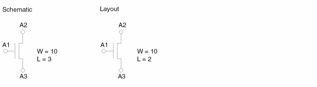
Besides comparing two networks, LVS also compares device subtypes (NMOS versus PMOS in CMOS circuits) and some device parameters, such as channel width and length in MOS circuits.
The LVS tool includes sections for checking
Layout Versus Layout
Layout versus Layout (LVL) is the portion of LVS that compares two similar mask layout databases at the device or gate level and reports discrepancies in the interconnections and in certain device parameters. LVL requires the LVL-PART command in the Description block. For more information about LVL, refer to the
Schematic Versus Schematic
Schematic versus Schematic (SVS) is the portion of LVS that compares two schematics. SVS requires the following commands in the Description block:
For more information about SVS, refer to the
Hierarchical Layout Versus Schematic
Hierarchical Layout Versus Schematic (HLVS) works like LVS, except that it operates on a two-level hierarchy. For more information about HLVS, refer to the
Initial Correspondence Node Pairs
You can provide a set of initial correspondence nodes as starting points for the LVS trace operation. When a node in the layout database and a qualified node in the schematics have identical, unique labels, they become an initial correspondence node pair. A qualified schematic node is either a power node, ground node, top-level input node, top-level output node, or, depending on the schematic netlist language being used, an internal node. For details about assigning initial correspondence node pairs for the schematic netlist, refer to the "Compiling Network Descriptions (LOGLVS)" section in Chapter 5.
LVS chooses all power nodes, ground nodes, clock nodes, and at least one other node as minimum initial correspondence nodes. Because the program uses these initial correspondence pairs for trace operations, the more initial correspondence node pairs you provide, the more efficient the trace can be. However, LVS never questions the match of any correspondence node pairs, and if there are any errors in the initial correspondence node pairs, the program cannot check them, and the trace operation can be misled. Because manual texting on the layout database is an error-prone process, you need to provide the minimum number sufficient to do an effective check. As a guideline, assign all pads as initial correspondence node pairs. Additionally, you need to include important signal nodes, nodes with many device connections, or nodes of highly parallel circuits.
If Dracula does not find initial correspondence points, it turns on an automatic matching capability. For more information about automatic matching, refer to the
Trace and Discrepancy Points
Starting from the initial correspondence node pairs, LVS traces the extracted layout network and the schematic network one step at a time. Initially, LVS matches all correspondence node pairs. Whenever LVS finds a unique match between layout and schematic, it defines the objects as matched nodes or devices.
LVS ends the trace operation when it matches all nodes and devices or when discrepancies have stopped tracing all paths. This means that discrepancy points are the focus points for error isolation and error interpretation, instead of unmatched nodes or devices. To present the discrepancies, LVS reports matched or unmatched nodes and devices related to particular discrepancies. The number of unmatched devices or nodes are not necessarily the same as the number of discrepancy points.
The sequence of the trace is dynamically determined in the program. Because error interpretations based on these assumptions might be incorrect, do not assume any trace sequences.
Using LVS
This section describes the following functional flow for using LVS:
- Run DRC and ERC and correct all errors.
- Compile the schematic netlist using LOGLVS.
- Check the layout text.
- Create and compile a rules file.
- Run LVS.
- View the discrepancy report.
Running DRC and ERC
You can run multiple verification operations such as DRC, ERC, LVS, and LPE at the same time. However, it is usually better to run operations one at a time, so you can correct only one type of error at a time. If you run ERC on the layout database first, you can correct the errors detected and reduce the run time and number of LVS discrepancies you must correct. When you run an ERC check, keep the following in mind:
- Check for illegal devices such as MOS diffusion connections to more than two electrical nodes or no electrical node.
- Using the MULTILAB command, check for shorted circuits between pads and major signals, such as VCC and VSS.
- Using the SAMELAB and ELCOUNT commands, check for open circuits associated with pads or major signals.
- Check text on the layout. Use composite text only, not cell level text.
- Identify major nodes and attach text to them if necessary. (This applies to nodes that connect to more than 150 elements.)
Compiling the Schematic Netlist
See the
Checking the Layout Text
You can provide a set of initial correspondence nodes as starting points for the tracing operations or use the AUTOMATCH command for internal correspondence point matching. Supply initial correspondence nodes by placing text on the layout database or by supplying text using an EDTEXT file. For detailed information about texting the layout, refer to
When texting the layout, keep in mind the following guidelines:
- Text all input and output pads.
- Text power and ground nodes.
- Text important internal nodes.
- Make sure that the text strings on the database are the same as the node names in the netlist.
- Do not use too many texts per node.
- Check that the text origin is inside or at the edge of the geometry.
Creating and Compiling an LVS Rules File
If you have already run ERC, you can add LVS commands to your existing rules file. You can find a full description of each command in the “Description Block Commands” and “Operation Block Commands” chapters.
The following LVS commands are required:
Calls the schematic netlist file created by LOGLVS. Enter this command in the Description block.
Extracts the layout database for a consistency check between layout and schematic. Enter this command in the Operation block.
The following Description Block commands are optional:
Inputs a file containing initial correspondence points for LVS matching. Lets you input initial correspondence points when node text names are different on the layout and schematic netlists. Lets you supply low-level net names as initial correspondence points.
Sets filter options for both the layout and schematic.
Sets filter options for the layout.
Sets filter options for the schematic.
Specifies LVS report options, letting you select the LVS error types you want listed.
Generates a new LVS report from a previous LVS run.
Lets you smash parallel capacitors even if they are of different types.
Removes
After you create the LVS rules file, use PDRCULA to compile it. When the file is free of errors, you can run an LVS check.
Running LVS
Submit the LVS rules file using the jxsub.com command.
Viewing the LVS Report
Dracula creates a file containing all discrepancies found during the LVS comparison. The file name is printfile.lvs, where printfile is the name assigned by the PRINTFILE command in the Description block. Refer to later sections of this chapter for descriptions of the error messages and discrepancies.
LVL Overview
This section presents an overview of Layout Versus Layout (LVL) and rules files to demonstrate the verification of two similar IC layout databases. The output is in both graphic and listing formats.
LVL is the portion of LVS that compares one IC layout to a similar IC layout on the device/gate level (not on geometric polygon data) and reports discrepancies in the interconnections. (To compare polygon data from different layout databases, use the EXPORT and IMPORT commands with the logical NOT or XOR commands.) The system automatically generates the layout networks when you use the SCHEMATIC and GRAPHICS options for the LVL-PART command. LVL accepts layout databases from major CAD graphics systems.
In addition to the two layout networks (6NET files), the system produces a list of corresponding nodes for power, ground, clocks, inputs, and outputs (6PAD files) through the texting facility on both layouts. The texting on both layout databases must be the same.
LVL converts each network into internal model format (6NET files). Starting from the inputs and outputs of the layout circuit, LVL traces the two circuit models. Because the trace algorithm moves one step at a time, LVL uses heuristics. LVL traces all I/O’s of the layout circuit and then traces the paths that require less backtracking. When the trace detects a match, LVL assigns a matched status to the devices or nodes. When the trace detects a mismatch, LVL stops tracing the path for that particular I/O.
If LVL assigns all devices and all nodes a matched status and there are no discrepancy points in the traced paths, the two layout networks are consistent. If LVL detects discrepancies, the system presents all discrepancy points in the printfile.lvl output listing.
In addition, LVL compares device subtypes and certain device parameters, such as the channel width and length of MOS devices.
Preparing for LVL
Before running LVL, perform the following steps:
- Run ERC checks on both layout databases as follows:
- Create a rules file for the reference layout database. This LVL rules file is the ERC rules file with the following two additions:
-
Create a second rules file for the second layout database. Modify the ERC rules file as follows:
- Specify LVL-PART=GRAPHICS in the Description block.
-
Specify the LVSCHK command at the end of the Operation block to start the LVL check of the reference layout database against the layout database.
The LVL run provides a printfile.lvl discrepancy listing and lvlplot graphic output database in the file specified by the OUTDISK command.
The LVL discrepancy listing is similar to the LVS discrepancy listing except that the program lists the x,y locations for the device in the reference layout database. LVL also lists device subtypes and substrate connections. If you specify the proper LVSCHK options, LVL checks and lists MOS channel width and lengths.
-
To submit and execute the two LVL rules files, use the /NEXT command in the preprocessor.
The LVL-PART command alerts the preprocessor that LVL is performing an LVL discrepancy check. Because the LVL job is similar to an LVS job, use /NEXT to combine the two LVL rules files. -
To control the formation of pseudo devices in the MOS process and to check MOS device sizes, use LVSCHK options.
If you do not specify lvschk options exactly the same in both rules files, the consistency check is different.
Rules Files
The following are examples of rules files to submit LVL runs. You can enter command names in either lowercase or uppercase letters.
Rules File for the Schematic
; **** "LVL1.COM" rules file for the Reference Layout ****
; ****                    Device (LVL-PART) ****
; **** NOTE: To run LVL, the consistency check must be ****
; **** between two (2) similar (process technology) ****
; **** databases. ****
;
;
*DESCRIPTION
.
PRIMARY = top1
MODE = exec now
SYSTEM = gds2
SCALE = .001 mic
RESOLUTION = .25 mic
PROGRAM-DIR = drac:
OUTDISK = lvllout
.
.
INDISK = layout1.in  ;database for the reference device (SCHEMATIC)
PRINTFILE = lvllprt  ;print file for the reference device run
LVL-PART = schematic ;specifies as LVL reference device
.
.
*END
*INPUT-LAYER
pwell = 1
ndiff = 2
pdiff = 3
poly = 4
contact = 5
metal = 6 TEXT = 26
pad = 7
SUBSTRATE = bulk 99
CONNECT-LAYER = nsub pwell psd nsd poly metal
*END
*OPERATION
AND poly ndiff ngate ; n-channel devices
NOT ndiff ngate nsd  ; N source/drain diffusion
AND poly pdiff pgate ; p-channel device
NOT pdiff pgate psd  ; P source/drain diffusion
NOT bulk pwell nsub  ; N substrate
AND nsd nsub ntsub   ; pseudo contact for N substrate
AND psd pwell ptwell ; pseudo contact for P well
;
CONNECT metal poly BY contact ; connecting the conductor
                              ; layers by contact
CONNECT metal nsd BY contact
CONNECT metal psd BY contact
CONNECT psd pwell BY ptwell
CONNECT nsub  nsd BY ntsub
;
ELEMENT MOS[n] ngate poly nsd pwell ; n-channel ELEMENT
ELEMENT MOS[p] pgate poly psd nsub ; p-channel ELEMENT
ELEMENT PAD    pad   metal ; pad ELEMENT
;
MULTILAB OUTPUT  shorts  40 ; run the “shorts” test
SAMELAB  OUTPUT  opens   40 ; run the “opens” test
LVSCHK                      ; specify the LVL check
*END
Rules File for Graphics
; ****   "LVL2.COM" rules file for the Layout Device ****
; ****   to be checked (LVL-PART=GRAPHICS)   ****
; ****   NOTE: To run LVL, the consistency check must be ***
; ****   between two similar (process technology) databases*
;
*DESCRIPTION
.
PRIMARY = top2
MODE = exec now
SYSTEM = gds2
SCALE = .001 mic
RESOLUTION = .25 mic
PROGRAM-DIR = drac:
OUTDISK = lvl2out
.
.
INDISK = layout2.in ; database for the device to be checked
PRINTFILE = lvl2prt ; print file for the device to be checked
LVL-PART = graphics ; specifies as LVL device to be checked
.
.
*END
*INPUT-LAYER
pwell = 21
ndiff = 7
pdiff = 22
poly = 24
contact = 5
metal = 10 TEXT = 13
pad = 63
SUBSTRATE = bulk 99
CONNECT-LAYER = nsub pwell psd nsd poly metal
*END
*OPERATION
AND poly ndiff ngate ; n-channel devices
NOT ndiff ngate nsd  ; N source/drain diffusion
AND poly pdiff pgate ; p-channel device
NOT pdiff pgate psd  ; P source/drain diffusion
;
NOT bulk pwell nsub  ; N substrate
AND nsd nsub ntsub   ; pseudo contact for N substrate
AND psd pwell ptwell ; pseudo contact for P well
;
CONNECT metal poly BY contact ; connecting the conductor
                              ; layers by contact
CONNECT   metal   nsd   BY contact
CONNECT   metal   psd   BY contact
CONNECT   psd     pwell BY ptwell
CONNECT   nsd     nsub  BY ntsub
;
ELEMENT MOS[n] ngate poly nsd pwell ; n-channel ELEMENT
ELEMENT MOS[p] pgate poly psd nsub  ; p-channel ELEMENT
ELEMENT PAD  pad  metal             ; pad ELEMENT
;
MULTILAB  OUTPUT  shorts  40        ; run the "shorts" test
SAMELAB   OUTPUT  opens   40        ; run the "opens" test
;
LVSCHK                              ; specify the LVL check
;
*END
Running LVL
To start an LVL run on a UNIX workstation, type the following command:
% PDRACULA
: /GET LVL1.COM
: /NEXT
: /GET LVL2.COM
: /FIN
LVL runs lvl1.com, then runs lvl2.com. The LVL discrepancy report file is lvl2prt.lvl.
SVS Overview
Schematic Versus Schematic (SVS) compares two schematics. The two schematics must be in different directories. SVS requires the following commands in the Description block:
- SVS-LAYOUT specifies the layout data file generated by LOGLVS.
- SVS-SCHEMATIC specifies the schematic data file generated by LOGLVS.
- HCELL-COLUMN-1 specifies whether the first column in the Hcell table lists layout or schematic cells. This command is required for hierarchical Dracula only.
For more information about these commands, refer to
Running SVS in Flat Mode
The following is an example of a rules file for flat mode SVS:
*DESCRIPTION
 PRINTFILE = lvsprt
 PROGRAM-DIR = /DRACULA/
SVS-SCHEMATIC = LVSLOGIC.DAT
SVS-LAYOUT = ../LVSLOGIC.DAT
*END
;
*OPERATION
 LVSCHK
*END
Running SVS in Cell or Composite Mode
Here is an example of a rules file for cell or composite mode SVS:
*DESCRIPTION
 PRINTFILE = lvsprt
 SVS-SCHEMATIC = LVSLOGIC.DAT
 SVS-LAYOUT = ../LVSLOGIC.DAT
 program-dir = /DRACULA/
 CHECK-MODE=comp
 HCELL-FILE=../cell.tab
*END
;
*OPERATION
 LVSCHK
*END
Running SVS in Hierarchical Mode
To run SVS in hierarchical mode, you must include the number 1 at the end of the LOGLVS CELL command. The number 1 identifies the first cell name in the Hcell file as a schematic. This example specifies that the first cell name listed in the Hcell file HCELL.TAB is a schematic.
CEL HCELL.TAB 1
If you do not include the HCELL-COLUMN-1 command, the default setting is LAYOUT. To switch the role of both circuits after running LOGLVS, use the HCELL-COLUMN-1 command. For example, on the first LOGLVS run, specify the command as follows:
SVS-SCHEMATIC = LVSLOGIC
SVS-LAYOUT = ../LVSLOGIC.DAT
One the second run, switch the circuits without rerunning LOGLVS. Modify the rules this way:
SVS-SCHEMATIC = ../LVSLOGIC.DAT
SVS-LAYOUT = LVSLOGIC.DAT
HCELL-COLUMN-1 = SCH
LVS Report Format
The following is a brief overview of a sample LVS report. An LVS report contains information pertaining to an LVS job run. Depending on whether you run flat, cell, or composite mode, some of the major sections in the LVS reports can be the following:
- Header: The header contains the version identification of Dracula, the execution time of the job, and the name of the primary cell. This section is created by PDRACULA.
- EXTERM: If you include the EXTERM-NOWARN=YES command in the Description block, only the “unconnected pins in cell” messages are not displayed in the LVS report. This section is for composite mode LVS.
- XDEVIC summary: Reports illegal hierarchical devices.
- LVSNET summary: LVSNET prints warning messages in this section.
- FILTER (layout) summary: FILTER prints a summary of statistics for the layout side in this section. If you specify special filter options, they are listed in this section.
-
REDUCE (layout) summary: This summary lists the options used in REDUCE. Depending on the FILTER-OPT command or the LVSCHK or LPECHK[F or G option] command, the schematic REDUCE or the layout REDUCE may be different. The device reduction statistics follow the options listing.
The following types are described in the “Device Recognition” section in this chapter:
PDW AND SDWI SMID NOR PUP OR PDWI PMID NAND SDW AOI SUPI MOS SUP OAI PUPI INV
MOSCAP represents the number of transistors reduced to MOS capacitors; that is, MOS transistors with source and drain tied together to either power or ground.
Other device types listed with statistics are the following:
BJT CELL DIODE LDD CAP UND RES BOXThe reference to “CELL” means the number of Hcells (placements or instances) that are placed in the network. “LDD” represents the lightly doped drain. “UND” represents the undefined device. For more information about “UND,” refer to the Device Recognition in LVS section in this chapter. -
FILTER (schematics) summary
FILTER prints a summary of statistics for the schematics side in this section. If you specify special filter options, they are listed in this section. -
REDUCE (schematics) summary
The statistics for the reduction of the schematics side are listed in this section. The meaning of each type of device is the same as the REDUCE (layout) section. -
Main LVS report body
This section is the core of the LVS report. It contains the date and time of execution of the LVS module and LVS options such as PRINTLINE, WPERCENT, and LPERCENT, the correspondence node pairs, LVS device match summary, the discrepancy points listing, the discrepancy points summary, the device matching summary by type, and the unmatched devices listing. -
Repeat summary
This section is at the end of the LVS report. It repeats the summary sections in the main report body to let you quickly browse LVS results.
Sample LVS Report
The following sample report shows sections that you might have in your LVS report.
*******************************************************************
*/N* DRACULA   (REV. 4.4.X / 4.4 /  GENDATE: 22-AUG-95/10)
*** (Copyright 1995, Cadence) ***
*/N* EXEC TIME =22:55:37 DATE =29-AUG-95
*******************************************************************
INDISK PRIMARY CELL :TEST
*********** LVSNET SUMMARY REPORT ***********
WEFFECT VALUE= 0.0000000
*********** EXTERM SUMMARY REPORT ***********
*CRCTEX* WARNING *--UNCONNECTED PINS IN CELL =    2  PLACE. =    31
PIN NAME     LAYER NAME     X          Y
Z2BAR        MET1         1344.00  -2402.40
******* FILTER (LAYOUT) SUMMARY REPORT *******
SET FILTERING OPTIONS TO BCDEFGHIJKO
ELIMINATED 509 OUT OF 1694 DEVICES FROM NETWORK
ELIMINATED 11 OUT OF 1185 DEVICES FROM NETWORK
******* REDUCE (LAYOUT) SUMMARY REPORT *******
******* STATISTICS BEFORE REDUCE ****
 MOS   BJT   RES   DIODE   CAP   UND   BOX   CELL   LDD
 1172   0     0      0       0     2     0      0     0
OPTION TO SMASH PARALLEL DEVICES IS -- ON
OPTION TO CONSTRUCT MOS PARALLEL/SERIES STRUCTURES IS -- ON
OPTION TO SMASH PSEUDO PARALLEL DEVICES IS -- OFF
OPTION TO FORM CMOS GATES IS -- OFF
OPTION TO FORM NAND/NOR GATES IS -- OFF
******* STATISTICS AFTER REDUCE ****
 MOS   BJT   RES   INV   DIODE   CAP   SDWI   PDWI   SUPI
113    0     0    102     0      0      2     13     13
PUPI  SDW   PDW   SUP   PUP     AND    OR     AOI    NAND
2     58    23    56     58      0      0      0      0
NOR   OAI   UND   BOX   CELL    LDD   SMID    PMID   MOSCAP
0      0     2     0      0      0      0      0      0
******* FILTER (SCHEMATIC) SUMMARY REPORT ****
SET FILTERING OPTIONS TO FGHIJKO
ELIMINATED 0 OUT OF 798 DEVICES FROM NETWORK
******* REDUCE (SCHEMATIC) SUMMARY REPORT ****
******* STATISTICS BEFORE REDUCE ****
 MOS  BJT  RES  DIODE  CAP  UND  BOX  CELL  LDD
798   0    0     0     0    0    0    0     0
******* STATISTICS AFTER REDUCE ****
 MOS     BJT    RES    INV    DIODE   CAP   SDWI   PDWI    SUPI
 107     0      0      102    0       0     2      13      13
 PUPI    SDW    PDW    SUP    PUP     AND   OR     AOI     NAND
 2       58     23     56     58      0     0      0       0
 NOR     OAI    UND    BOX    CELL    LDD   SMID   PMID    MOSCAP
 0       0      0      0      0       0     0      0       0
 ***************** LVS REPORT *****************
 DATE : 29-AUG-95
TIME : 22:57:57
 PRINTLINE = 1000
MOS DEVICE WIDTH NOT CHECKED
MOS DEVICE LENGTH NOT CHECKED
1 ***************************************************
********* CORRESPONDENCE NODE PAIRS **********
***************************************************
SCHEMATICS LAYOUT PAD TYPE
VDD    111 VDD           1   P
VSS    196 VSS           18  G
P1     188 P1            121 I
P10    2   P10           14  I
P11    388 P11           8   I
P12    368 P12           9   I
P13    392 P13           10  I
P14    364 P14           33  I
P15    396 P15   61  I
P16    372 P16   95  I
P17    400 P17   125 I
P18    376 P18   166 I
P19    1   P19   215 I
P2     183 P2    110 I
P21    404 P21   294 I
P22    380 P22   328 I
P23    8   P23   337 I
P24    4   P24   301 I
P25    143 P25   336 I
P26    138 P26   335 I
P27    133 P27   334 I
P28    128 P28   333 I
P29    123 P29   332 I
P3     178 P3    79  I
P30    118 P30   331 I
P31    113 P31   330 I
P32    107 P32   329 I
P33    9   P33   405 I
P34    6   P34   258 I
P35    10  P35   327 I
P36    7   P36   305 I
P37    5   P37   321 I
P38    384 P38   293 I
P39    3   P39   224 I
P4     173 P4    2   I
P5     168 P5    3   I
P6     163 P6    4   I
P7     158 P7    5   I
P8     153 P8    6   I
P9     148 P9    7   I
 NUMBER OF LAY. PADS READ = 40   DISCARDED = 0
NUMBER OF SCH. PADS READ = 40   DISCARDED = 0
NUMBER OF VALID CORRESPONDENCE NODE PAIRS = 38
1 ***************************************************
********** LVS DEVICE MATCH SUMMARY **********
***************************************************
NUMBER OF UN-MATCHED SCHEMATICS DEVICES = 0
NUMBER OF UN-MATCHED LAYOUT DEVICES = 8
NUMBER OF MATCHED SCHEMATICS DEVICES = 434
NUMBER OF MATCHED LAYOUT DEVICES = 434
1 ***************************************************
********** DISCREPANCY POINTS LISTING **********
***************************************************
*********** DISCREPANCY 1***********************
--- NODE C59
---WITH EXTRA LAY DEVICES--------
OCCURRENCE NAME C72.4
 DEV926 PDW :            DEV1805   PDW X=794 Y=1206
C72.4, C59, I509   C72.4, C59, I509
 DEV927 SUP :            DEV1806   SUP X=852 Y=1222
C72.4, C59, I509   C72.4, I509, C59
OCCURRENCE NAME C59
 DEV928 SUP :            DEV1794  SUP X=2252 Y=2342
C59, P26, P26      C59, P26, P26
 DEV773 MOS N NOR M3 :   DEV1543   MOS N X=2194 Y=2342
P26, C59, VSS      P26, VSS, C59
OCCURRENCE NAME C64
DEV1055 PDWI :           DEV1938   PDWI X=2594 Y=2182
C64, C59, C60      C64, C59, C60
 DEV1057 SUPI  :         DEV1940   SUPI X=2652 Y=2182
C64, C59, C60      C64, C59, C60
OCCURRENCE NAME C72.7
 DEV1095 SDW :           DEV1786   SDW X=794 Y=1142
C72.7, C72.3, C59  C72.7, C59, C72.3
 DEV1096 PUP :           DEV1787   PUP X=852 Y=1126
C72.7, C72.3, C59  C72.7, C72.3, C59
OCCURRENCE NAME C64
 DEV1130 SDW :           DEV1967   SDW X=2594 Y=2262
C64-4, C59, C60    C64-4, C59, C60
 DEV1131 PUP :           DEV1968   PUP X=2652 Y=2246
C64-4, C60, C59    C64-4, C60, C59
***** UN-MATCHED ***** : ?DEV685 MOS P X=2452 Y=2278 C59, VDD, ?2192
***** UN-MATCHED ***** : ?DEV1523 MOS N X=2394 Y=2278 C59, VSS, ?2548
TOTAL 1 DISCREPANCY POINTS REPORTED
1 ***************************************************
********** DISCREPANCY POINTS SUMMARY **********
***************************************************
1 MATCHED NODE TO EXTRA LAYOUT DEVICES
***************************************************
******** DEVICE MATCHING SUMMARY BY TYPE ********
***************************************************
TYPE   SUB-TYPE  TOTAL DEVICE    UN-MATCHED DEVICE
                 SCH.    LAY.    SCH.    LAY.
MOS      P       399      404     0       5
MOS      N       366      367     0       1
1 ***************************************************
********** UN-MATCHED LAYOUT DEVICES **********
********** (LIST UP TO 100 ) **********
***************************************************
   : ?DEV491   MOS P X=2934 Y=1806
      VSS, VDD, ?231
   : ?DEV492   MOS P X=2950 Y=1822
     VSS, ?231, ?234
   : ?DEV493   MOS P X=2966 Y=1838
      VSS, ?234, ?243
   : ?DEV504   MOS P X=2982 Y=1854
      VSS, VDD, ?243
   : ?DEV685   MOS P X=2452 Y=2278
      C59, VDD, ?2192
   : ?DEV1523  MOS N X=2394 Y=2278
      C59, VSS, ?2548
1 ***************************************************
********** LVS SUMMARY (REPEATED) **********
***************************************************
***************************************************
********** LVS DEVICE MATCH SUMMARY **********
***************************************************
NUMBER OF UN-MATCHED SCHEMATICS DEVICES = 0
NUMBER OF UN-MATCHED LAYOUT DEVICES = 8
NUMBER OF MATCHED SCHEMATICS DEVICES = 434
NUMBER OF MATCHED LAYOUT DEVICES = 434
***************************************************
********** DISCREPANCY POINTS SUMMARY **********
***************************************************
1 MATCHED NODE TO EXTRA LAYOUT DEVICES
***************************************************
******** DEVICE MATCHING SUMMARY BY TYPE ********
***************************************************
 TYPE   SUB-TYPE       TOTAL DEVICE      UN-MATCHED DEVICE
                       SCH.    LAY.      SCH.    LAY.
 MOS       P           399     404        0      5
 MOS       N           366     367        0      1
Discrepancy Report Conventions
LVS follows these conventions when listing the discrepancy report.
Number of matched and unmatched devices
LVS highlights the number of matched and unmatched devices. The total device count might not be the same as the total number of extracted devices because LVS can combine multiple devices into pseudo-devices and smash parallel devices into a single device.
Schematic section against layout section
LVS divides an 80-column print line for a discrepancy point into two sections. The first 40 columns are the schematic section and the remaining columns are the layout section.
Schematic Section : Layout Section
Matched node identification
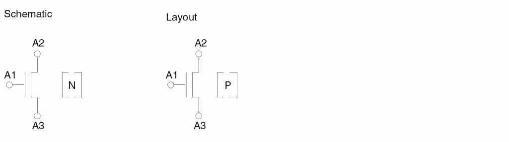
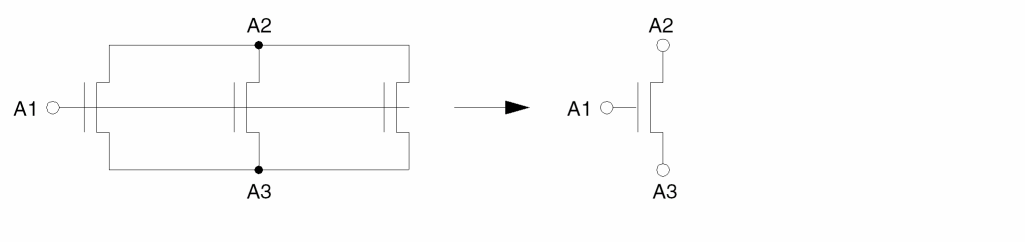
Use the schematic node name for both the schematic and layout nodes. If the schematic node is the local node, LVS uses the hierarchical node name from macro expansion to guarantee its uniqueness. For example, the following two-input NAND gate has five nodes with node 1 as the local node.
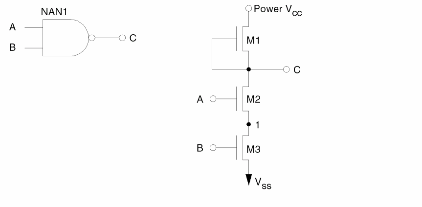
These six node names are VCC, VSS, A, B, C, and NAN1-1, where NAN1 is the occurrence name of the NAND gate and NAN1-1 is the node name for node 1 after macro expansion.
Unmatched schematic node identification
If LVS finds a node in the schematic that does not have a corresponding layout node, LVS prefixes the node with a question mark (?). For example, ?A, ?B, ?C.
Matched device identifications
LVS always lists matched devices side by side with a schematic device on the left side of the center colon (:) and a layout device on the right side of the colon. Both the schematic device and the layout device have a unique internally generated device number, followed by a device type and an optional device subtype. A schematic device can also have a logic gate type and a device name within that particular gate, if applicable. A layout device has x or y locations in a natural unit.
LVS then follows the list of nodes connected to the matched device. For example:
Occurrence Name     NAN1
DEV123  MOS  D  NAND   M1 :  DEV255  MOS D  X=100  Y=50
C,C,VCC                      C,C,VCC
Note that the schematic device name is local to the gate, so LVS lists the occurrence name whenever possible to uniquely identify the device on schematics. In the above example, M1 is the device within gate NAND with the occurrence name NAN1.
Unmatched schematic device identifications
If LVS finds a schematic device that is not referenced in the layout, LVS prefixes the device number with a question mark (?) and the corresponding layout device is (*****UNMATCHED*****).
?DEV123 MOS D NAND M1 : *****UNMATCHED*****
Unmatched layout device identification
If LVS finds a layout device that is not referenced in the schematic, LVS prefixes the device number with a question mark (?) and the corresponding schematic device is (*****UNMATCHED*****).
*****UNMATCHED***** ?DEV255 MOS D X=100 Y=50
| Device type | Terminals listed |
|---|---|
LVS Error Types
Discrepancy points are the focus points for all LVS error isolations. Depending on the LVS error type, one discrepancy point can involve a single node, single device, or a subcircuit (group of nodes and devices). LVS lists each discrepancy point separately, and it always corresponds to one LVS error. If a subcircuit is involved in a discrepancy point, not all nodes and devices are necessarily in error.
The Dracula program defines LVS errors for each discrepancy point based on its key device or node against the rest of the nodes and devices. Note that LVS errors do not necessarily correspond exactly to human perception of errors. For example, when two signal lines swap for a portion of the interconnects and are considered only one error, LVS might generate two discrepancy points, one for each signal.
LVS categorizes discrepancies into the following 15 error types:
| Type | Error description | Plot | Listing |
|---|---|---|---|
|
Device power connection mismatch (Multi-power supply situation) |
|||
LVS Error Type 1
Key: matched node Listed output: yes Graphic output: matched layout node
Initial correspondence nodes are not connected to devices. This is caused by misplaced layout text or input protection devices that are not properly defined.
LVS Error Type 2
Matched device to unmatched node.
Key: matched device Listed output: yes Graphic output: matched layout device, unmatched layout node
The device and some of its nodes are matched, but discrepancies are detected on other nodes.
LVS Error Type 3
Inconsistently matched device.
Key: matched device Listed output: yes Graphic output: matched layout device, matched layout node
The device or nodes are matched locally first, and global discrepancies are detected later.
LVS Error Type 4
Matched node to extra layout devices (missing schematic devices).
Key: matched node Listed output: yes Graphic output: matched layout node, unmatched layout device
Extra layout devices are connected to the key matched node in addition to a number of matched devices.
LVS Error Type 5
Matched node to extra schematic devices (missing layout devices).
Key: matched node Listed output: yes Graphic output: matched layout node
Extra schematic devices are connected to the key matched node in addition to a number of matched devices.
LVS Error Type 6
Matched node to unmatched layout and schematic devices.
Key: matched node Listed output: yes Graphic output: matched layout node, unmatched layout devices
Some of the schematic devices connected to the key matched node cannot be matched to the layout devices connected to the same node.
LVS Error Type 7
Other unmatched layout devices.
Key: unmatched layout devices Listed output: yes Graphic output: unmatched layout device
Unmatched layout devices are either totally separated from the rest of the circuit and cannot be reached from any initial correspondence node pairs or totally blocked by discrepancy points when trace operation stops.
LVS Error Type 8
Other unmatched schematic devices.
Key: unmatched schematic device Listed output: yes Graphic output: no
Unmatched schematic devices are either totally separated from the rest of the circuit and cannot be reached from any initial correspondence node pairs or totally blocked by discrepancy points when trace operation stops. These devices are listed at the end of the discrepancy point listing.
LVS Error Type 9
Key: matched device Listed output: yes Graphic output: matched layout device
Two matched devices have different subtypes, which could be the implant types in the MOS circuit.
LVS Error Type 10
Key: matched MOS device Listed output: yes Graphic output: matched layout device
Layout device size differs from the schematic device size by a specified percentage according to the LVSCHK command options WPERCENT and LPERCENT.
LVS Error Type 11
Key: matched MOS device Listed output: yes Graphic output: matched MOS devices
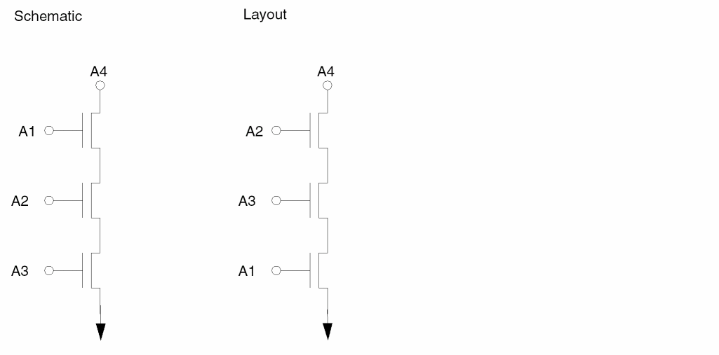
The physical locations of the layout MOS devices relative to outputs do not conform to the order specified in schematics.
LVS Error Type 12
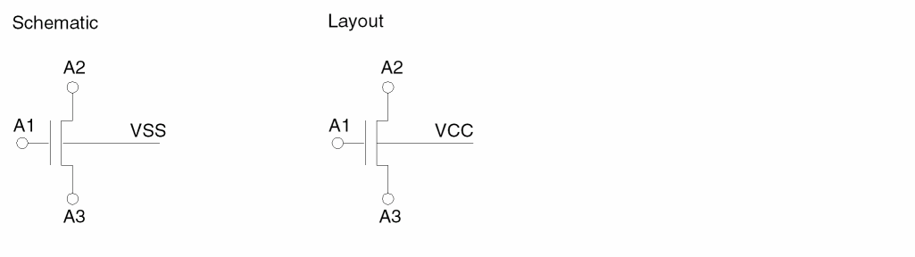
Device substrate connection mismatch.
Key: matched MOS device Listed output: yes Graphic output: matched MOS device
MOS substrate connections are different between layout and schematic devices. This error usually applies to the CMOS circuit.
LVS Error Type 13
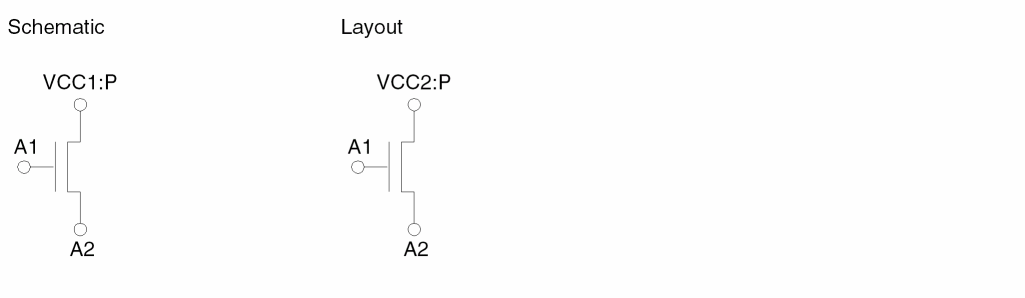
Device power connection mismatch.
Key: matched device Listed output: yes Graphic output: mismatched layout device
An incorrect power supply drives an output node in a multiple power supply situation.
LVS Error Type 14
Reduced layout parallel MOS devices.
Key: no Listed output: no Graphic output: reduced layout MOS devices
When the LVSCHK[K] option (keep parallel) is not turned on (as default for circuits), parallel MOS transistors are reduced into one MOS transistor. The remaining MOS transistors are not traced by LVS and are flagged as LVS error type 14. This condition should not be interpreted as an error.
LVS Error Type 15
Filtered out layout MOS devices.
Key: no Listed output: no Graphic output: filtered out MOS devices
When the LVSCHK[F] option (CMOS gate array filter) is turned on, unused CMOS devices are filtered out by LVS. Those devices can be flagged as LVS error type 15. Do not interpret this condition as an error.
Device Recognition in LVS
LVS recognizes two levels of devices. At the lowest level are all physical devices, such as MOS transistors, bipolar NPN transistors, bipolar PNP transistors, diodes, resistors, and capacitors. Second-level devices (pseudo gates and gates) are based on physical devices satisfying certain circuit structures. Typically, LVS uses a combination of both levels of devices in the trace operation. Therefore, the discrepancy points usually also include a combination of both levels of devices. LVS recognizes the logic gates and pseudo gates described in the following sections.
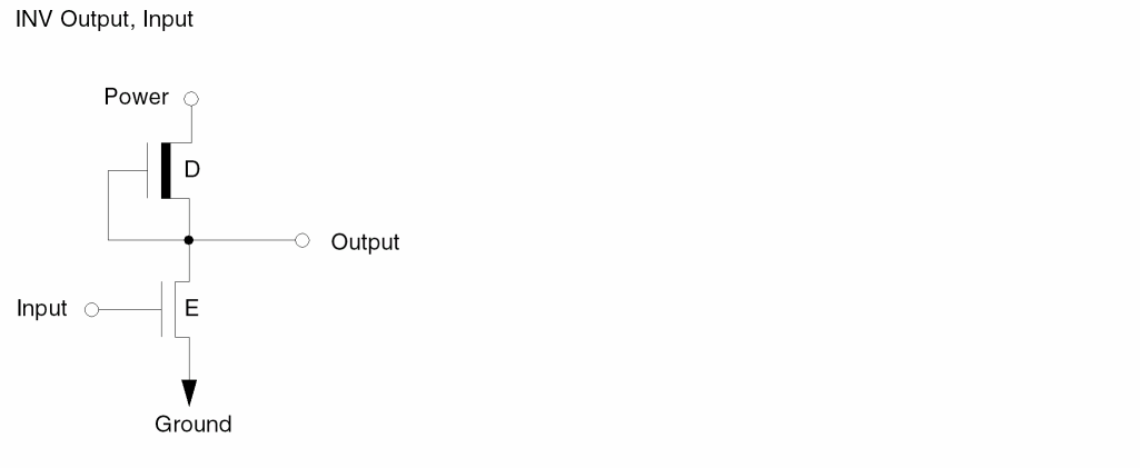
NMOS Inverter
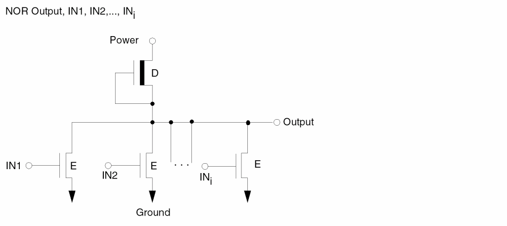
NMOS NOR Gate
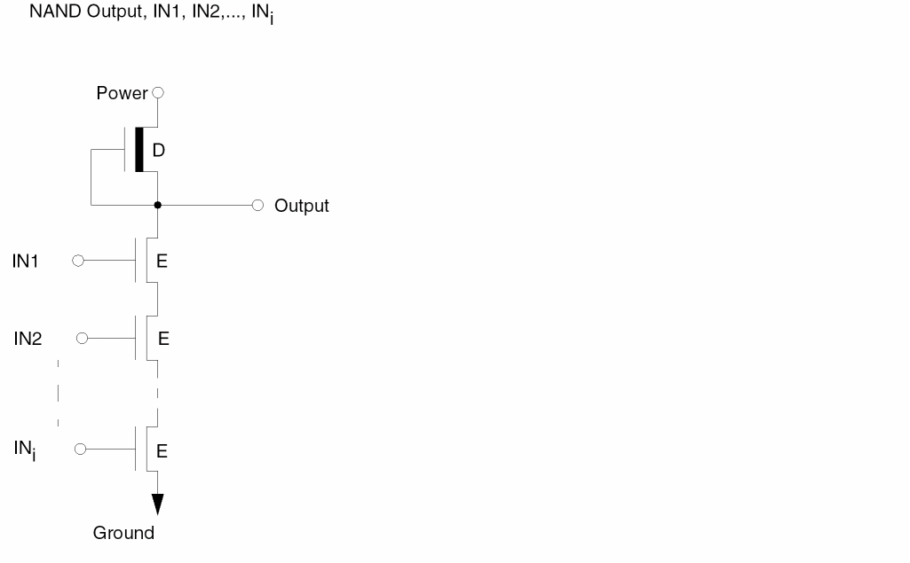
NMOS NAND Gate
CMOS Inverter
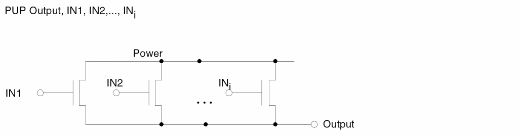
Simple Parallel Pull-Up (PUP) Structure
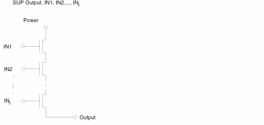
Simple Series Pull-Up (SUP) Structure
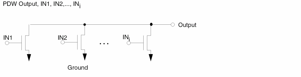
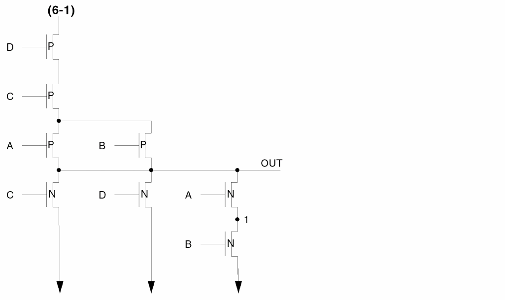
Simple Parallel Pull-Down (PDW) Structure
Simple Series Pull-Down (SDW) Structure
Complex Gate Including PUPI, SUPI, PDWI, and SDWI
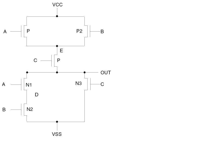
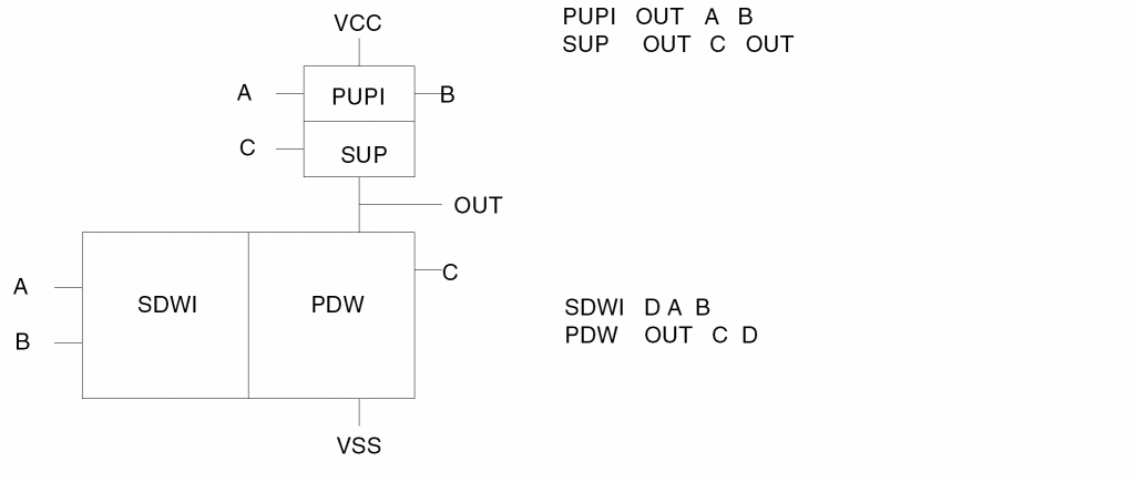
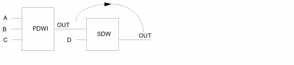
Parallel pull-ups and pull-downs and series pull-ups and pull-downs are element structures of complex gates. When LVS encounters a complex structure, it first recognizes and represents the devices in the innermost structure, then uses these devices to drive the outer structure to form a cascaded structure of these elements. In the following example, CMOS circuit devices 1 and 2 form a PUPI element that together with device 3 form a SUP element driving the output node. Devices 4 and 5 form a SDWI element that together with device 6 form a PDW element driving the output node.
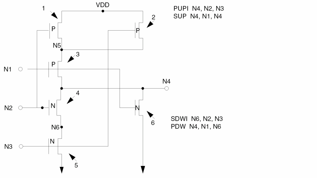
Because multiple series or parallel structures are involved in one complex structure, you must interpret the whole complex structure rather than just element structures in order to comprehend the true logic functions. In the outer structure (SUP and PDW in this example), LVS chooses the output node of the complex gate to represent itself. In the example, N4 is this node.
Inside a parallel structure, LVS chooses the internal nodes that are closest to the output node in order to represent the associated series substructure. LVS chooses N6 to represent the SDWI inside the parallel structure PDW.
Inside a series structure, LVS inherits its representation node to its parallel substructure. LVS chooses N4 to represent the PUPI under SUP. This process is applied from the outermost structure through the innermost structure.
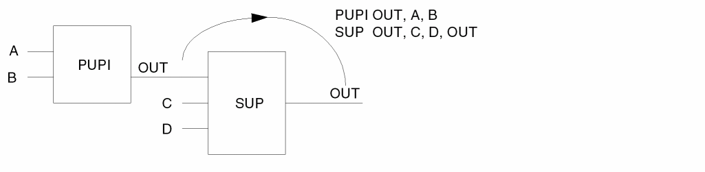
PUPI and SDWI
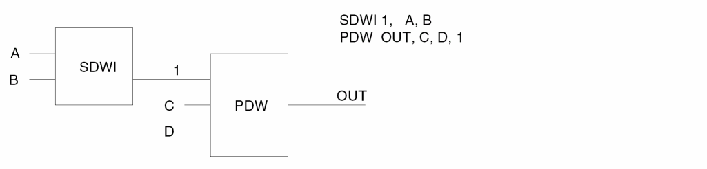
When PUP drives SUP, PUP is recognized as an incomplete PUP (PUPI) and the output node (in this example, OUT) is used as the output of the PUPI structure.
When SDWI drives PDW, use the internal node (in this example, D) to represent the output node of SDW that is recognized as an incomplete SDW (SDWI).
The pull-down elements for the complex structure are represented as follows:
SUPI and PDWI
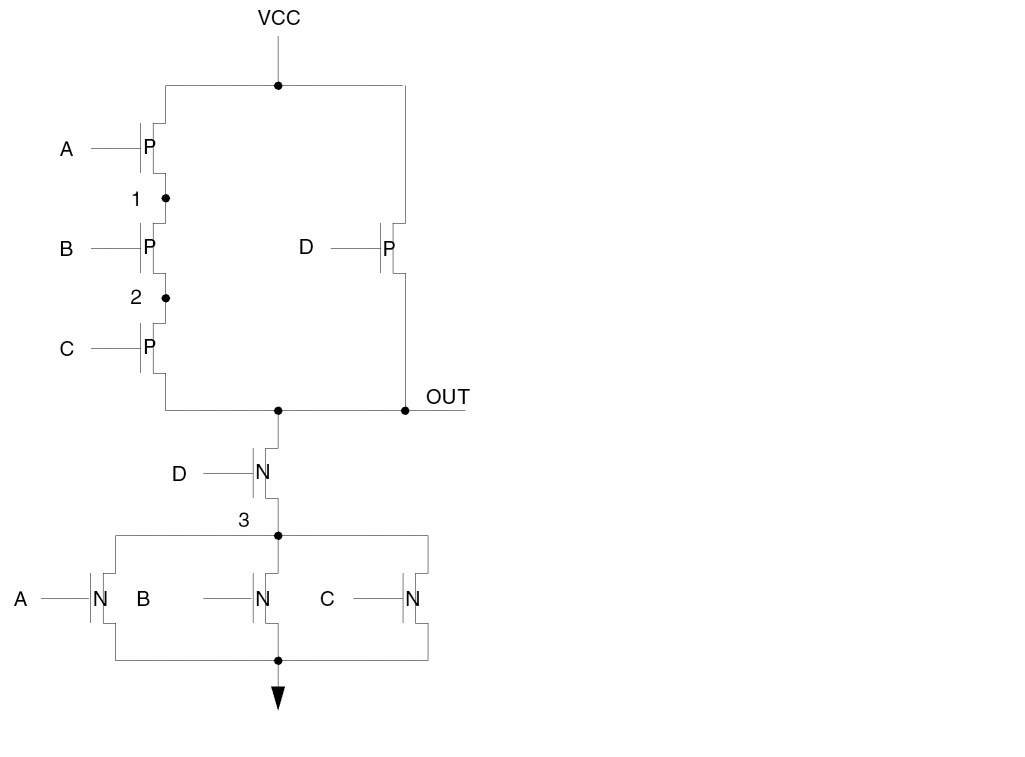
The pull-up elements for this complex structure are represented as follows:
When SUP drives PUP, use node 2 as the output node of the SUP structure, SUPI.
SUPI   2,    A,  B,  C
PUP    OUT,  D,  2
The pull-down elements for this structure are represented as follows:
When PDW drives SDW, use the output node of SDW to represent the output node of PDW, which is recognized as PDWI (incomplete PDW).
PDWI   OUT,  A,  B,  C
SDW    OUT,  D,  OUT
PUPI and SDWI
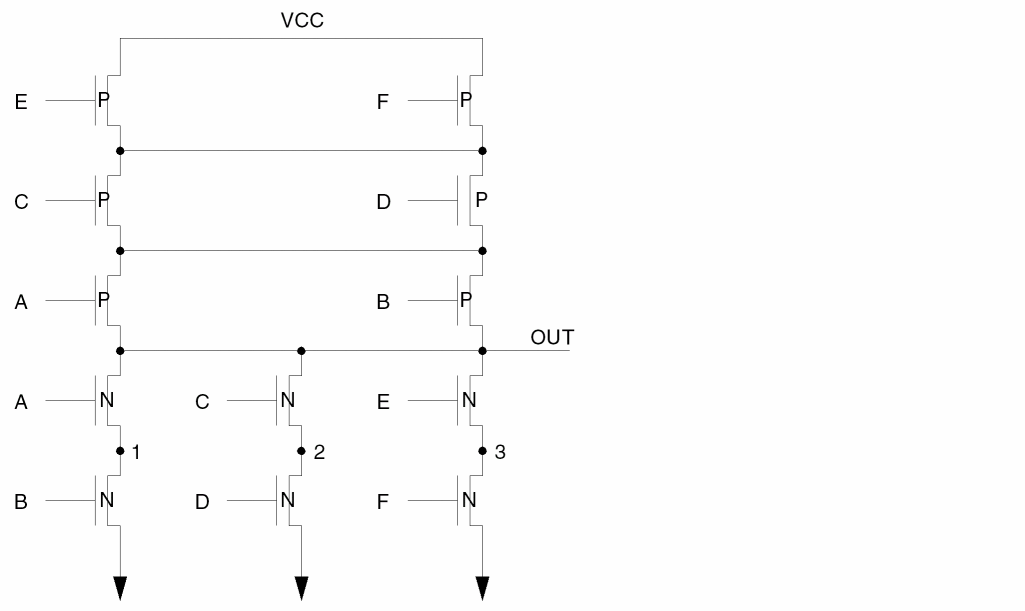
The pull-up elements for this complex structure are represented as follows:
The pull-down elements for this complex structure are represented as follows:
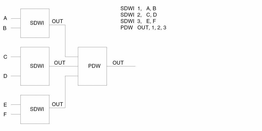
PUPI and SDWI
The pull-up elements for this complex structure are represented for as follows:
The pull-down elements for this complex structure are represented as follows:
SUPI and SDWI
For pull-up elements, the structure can be as follows:
For pull-down elements, the structure can be as follows:
CMOS NAND
CMOS NOR
CMOS AOI
CMOS AOIs
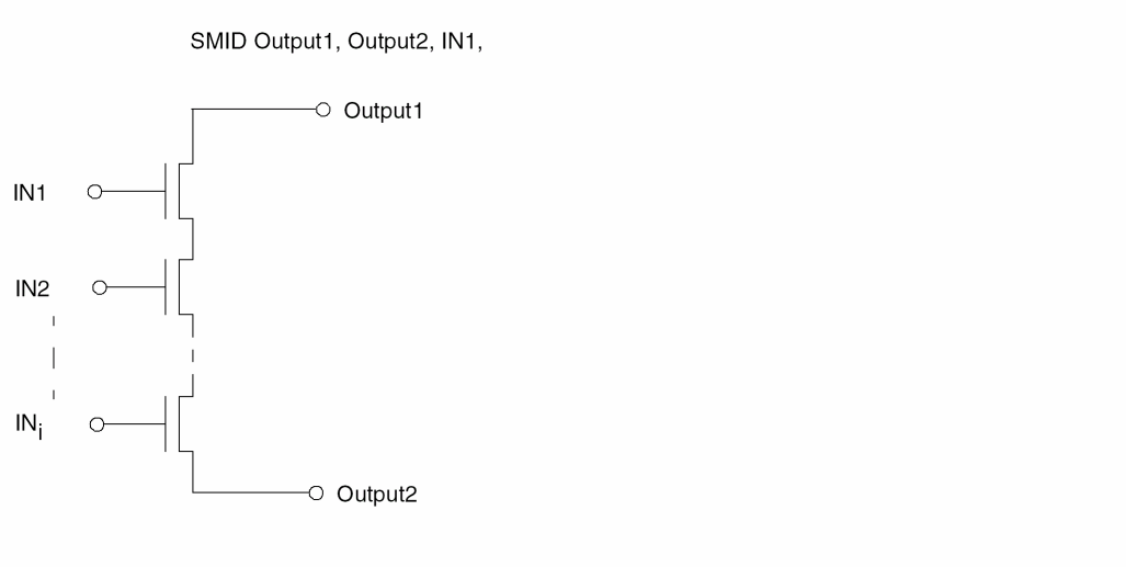
Simple Parallel Middle (PMID) Structure
This is a simple parallel middle (that is, neither pull-up nor pull-down, formed only when LVSCHK/LPECHK option [O] is used) structure of MOS transistors with the same implant.
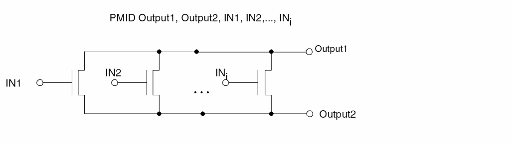
Simple Series Middle (SMID) Structure
This is a simple series middle (that is, neither pull-up nor pull-down, formed only when LVSCHK/LPECHK option O is invoked) structure of MOS transistors with the same implant.
Undefined Elements
In the circuit extraction process of the layout, any fixed terminal element that encounters an undefined number of terminals automatically becomes an undefined element in LVS and is listed with a question mark (?).
?MOS: A MOS transistor with more than two source or drain terminals.
?BJT: A bipolar transistor with more than one base terminal.
?RES: A resistor with more than two terminals.
?CAP: A capacitor with more than two terminals.
?DIO: A diode with more than two node terminals.
Isolating and Debugging Errors
LVS uses expanded node names and device names to identify the schematic node, device, or subcircuit in error. LVS also identifies the higher level gate or functional block, of which these devices are a part. For the layout devices, LVS prints x and y locations in natural units. Furthermore, LVS error types can generate graphic output, which in some cases points to errors more directly than listings (like showing the redundant errors of arrays). To isolate the errors, follow these steps:
- Focus on a discrepancy point. Identify its key device or node and understand the specific LVS error type.
- Locate schematic gates of the functional block by their expanded names and layout locations.
- Locate matched nodes or devices by their expanded names and layout locations.
- Interpret unmatched nodes or devices by LVS error types.
- Check the LVS graphic output by the same LVS error type.
- View the layout data on the graphic workstation to verify the findings, or use Dracula Interactive.
-
Inspect the Dracula log file for the following modules:
- The first REDUCE module reduces the layout side to second-level devices (logic gates and pseudo gates) for LVS discrepancy reporting. LVS lists a summary table of all devices at the end of this module. The summary is also included in the LVS report file.
- The second REDUCE module reduces the schematic side in the same manner as the layout side. If you compare the schematic summary table at the end of the REDUCE module in the log file, the total number of logic gates, pseudo gates, and MOS devices generated match with the layout summary. If there are fewer logic gates or pseudo gates, this usually means that power or ground was lost (or partially lost) in either the layout side or schematic side. For example, if the layout side has 100 more MOS devices and 30 fewer logic gates, you can assume that somewhere in the layout side there was a loss of power or ground. The ERC PATHCHK command can locate the nodes that are stuck or floating. The summary is also included in the LVS report file.
Interpreting an LVS Discrepancy
In this sample error summary file, discrepancies 1 and 2 are related. In discrepancy 1, LVS traces NODE 74 and in discrepancy 2, LVS traces NODE 84.
********************** DISCREPANCY 1 ************************
--------------- NODE 74 -----WITH EXTRA-LAYOUT DEVICES-----
OCCURRENCE NAME XEN1-10
DEV15    MOS P---MP2XEN13z   :  DEV572  MOS P  X=-322  Y=205
XEN1-10,  74,  XEN1-9        XEN1-10, XEN1-9, 74
OCCURRENCE NAME   84
DEV199   PUP                 :  DEV734  PUP    X=-170  Y=150
84, 85, 74, 96               84, 74, 85, 96
DEV201   SDWI                :  DEV738  SDWI   X=-170  Y=61
84, 95, 96, 74               97, 85, 96, 74
DEV200   SDWI                :  DEV737  SDWI   X=-31   Y=61
84, 85, 96, 74               98, 85, 96, 74
**** UN-MATCHED ****   DEV736  SDWI  X=-170  Y=72
                       99, 985, 96, 74
**** UN-MATCHED ***    DEV735  SDWI  X=-31   Y=72
                       100, 85,  96, 74
********************* DISCREPANCY 2 *************************
--------------- NODE 84 ---------------------------------
DEV199   PUP           :  DEV734   PUP   X=-170  Y=150
84, 85, 74, 96         84, 74, 85, 96
?DEV202   PDW          :  **** UN-MATCHED ****
84, 97, 98
**** UN-MATCHED ****   :  ?DEV741  PDW   X=-170  Y=14
                       84, 97, 98, 99, 100
DEV201   SDWI          :  DEV738   SDWI  X=-170  Y=61
97, 95, 96, 74         97, 85, 96, 74
DEV200   SDWI          :  DEV737   SDWI  X=-31   Y=61
98, 85, 96, 74         98, 85, 96, 74
**** UN-MATCHED ****   :  DEV736   SDWI  X=-170 Y=72
                       99, 985, 96, 74
**** UN-MATCHED ***    :  DEV735   SDWI  X=-31  Y=72
                       100, 85,  96, 74
The following is a schematic representation for discrepancy 1:
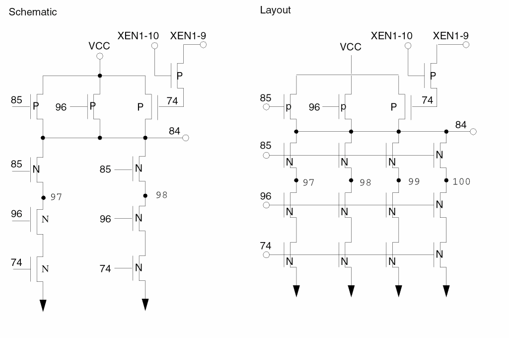
The schematic side has two SDWI gates in parallel. The layout side has four SDWI gates in parallel. Discrepancy 2 is the repetition of discrepancy 1 traced from nodes 74 and 84.
Logical Equivalence in MOS Digital Circuits
For certain digital MOS circuits, the physical order of the inputs to the gates of the MOS devices in series or parallel are interchangeable because they are logically equivalent. LVS handles logical equivalences through the recognition of logic gates and pseudo gates. All inputs to these gates are interchangeable. LVS recognizes logic gates and pseudo gates by default. To check the physical order of MOS devices, you can use the following methods:
- To stop the formation of logic gates and pseudo gates to force LVS to trace all MOS transistors individually, turn on the LVSCHK[X] option. This option is useful for analog circuits.
-
Use the special MOS element type ELEMENT MOS[X-] and specify the subtype of MOS CDL transistor card of type X* to stop the formation of logic gates and pseudo gates locally. For example:
M12 12 18 1 1 X*
where * is any alphanumeric character.
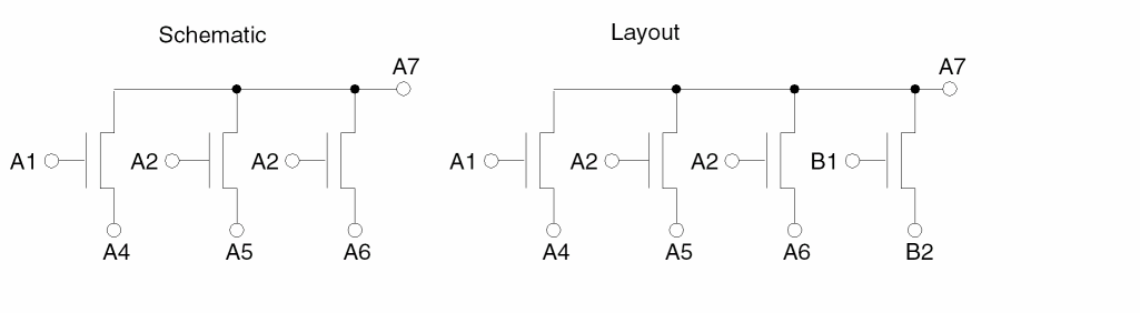
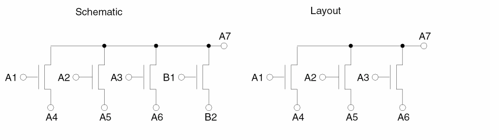
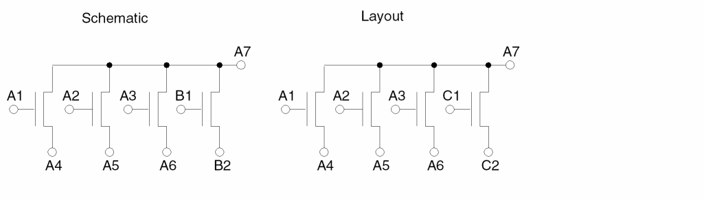
Calculations on Parallel MOS Devices for LVS
For some digital MOS circuits, you must place parallel transistors in the layout. Unless suppressed by an LVSCHK[K] option, the program smashes these devices into one transistor. This section describes the formula LVS uses to combine the transistor sizes of these parallel devices.
For parallel transistors, you must specify both length and width. If you do not specify either length or width, the length and width of the parallel transistors is 0, which means unspecified.
W/L Calculation
These formulas compute the width and length of the transistor that replaces a group of n parallel transistors as the result of the smashing operation.
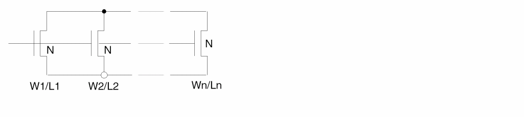
Compute the width and the length of the smashed transistor as follows:
where you compute the area, A = W*L, of the resulting transistor as the sum of the areas of the parallel transistors
and you compute the width/length ratio C = W/L of the resulting transistor as the sum of the width/length ratios of the parallel transistors.
This smashing operation preserves the electrical properties of the circuit.
For more information about the layout MOS device W/L calculation, refer to “LPE Overview”.
Weff MULDELW Calculation
Because of process variations such as optical, etching effects, and
implant/field oxide encroachment, you can compensate for changes in effective channel widths when laying out multiple parallel finger MOS transistors. Use the following equation to check schematic MOS device effective widths against compensated layout MOS device widths.
Weff = Wactual + (N-1) * MULDELW
The value for MULDELW is typically negative. The default is 0.
MULDELW modifies the effective width (Weff) of MOS devices that have multiple fingers in parallel. For both schematic devices and layout devices, calculate the effective widths as follows:
Weff = Wactual + (N-1) * MULDELW
- Weff is width used for LVS comparison.
- Wactual is sum of all widths of parallel fingered devices.
- N is the number of smashed parallel fingers of the transistor.
If a transistor has only one finger, then N=1 and Weff=Wactual as well. If you specify the K option, then N always is 1, because K prevents smashing of parallel legs of a device. If you specify the S option for split-gates, then N for these devices is calculated like normal parallel devices after these gates are smashed.
*OPERATION
.
.
LVSCHK   WPERCENT=2 MULDELW= -1
*END
Example 1
| Schematic | Layout | ||
Example 2
| Schematic | Layout | ||
Example 3
MOS Devices Without Substrate Terminal
Some MOS devices are defined without substrate terminal. Currently Dracula would automatically output 0 as the substrate terminal if it is not defined in the rule file for layout-only run or LVS run without the S option specified in LPESELECT. Users expect to see a netlist without substrate terminal output if the above situation happens. The 4.8 version provides a solution to this problem by providing a new command, NO-SUB-TERM in the Description Block to offer the capability of not defining a substrate when extracting a device using LPE.:
Command Syntax
NO-SUB-TERM=mos_subtype1{mos_subtype2,....mos_subtypen}
Arguments
is the sub-type of MOS which is specified in the ELEMENT MOS command. For example, "N" of the following element definition:
ELEMENT MOS[N] NDEVICE POLY NSD
The command would only be effective in the following condition, otherwise, it would be ignored:
Example
NO-SUB-TERM =N,P
.......
ELEMENT MOS[N] NGATE POLY NSD
ELEMENT MOS[P] PGATE POLY PSD
......
An output example may look like the following:
M1 OUT IN VDD P L=3.00U W=6.25U
M2 GND IN OUT N L=3.00U W=6.25U
Calculations on Parallel and Series Resistor Devices width/length for LVS
For some circuits, you have to place parallel or/and series resistors in the layout. Unless these are suppressed by an LVSCHK[K] option, Dracula smashes parallel devices into one resistor. LVSCHK[R] provides smashing series resistors into one resistor.
This section describes the expression LVS uses to estimate the effective resistor length (Leff) and width (Weff) when combining (or smashing) parallel and series resistors:
-
For parallel resistors the effective values are calculated by formulas:
Leff = SQRT(AREA/(W1/L1+W2/L2))
Weff = AREA/Leff
-
For series resistors the effective values are calculated by formulas:
Weff = SQRT(AREA/(L1/W1+L2/W2))
Leff = AREA/Weff
W1 - the width of the first resistor,
L1 - the length of the first resistor,
AREA1 - the area of the first resistor,
W2 - the width of the second resistor,
L2 - the length of the second resistor,
AREA2 - the area of the second resistor,
AREA - the calculation of the combined AREA is controlled by the RESWSMASH command (see “RESWSMASH”):
The calculations are provided step by step.
Bipolar LVS Example
The following is an example of an input rules file in bipolar technology.
;*****************************************************************
;                BIPOLAR LVS INPUT RULES FILE
;             P - SUBSTRATE AND DOUBLE LAYER METAL
;*****************************************************************
;         ************* TYPE OF DEVICES; ***********
;*
;* DEVICE/ELEMENT           TYPE
;* --------------           ----
;* NPN VERTICAL             [N]
;* PNP VERTICAL             [PV]
;* PNP LATERAL              [PL]
;* DIODE SCHOTTKY           [S]
;* CAPACITOR MET1/DEEP N+   [C]
;* RESISTOR DEEP N+         [DN]
;* RESISTOR SHALLOW P       [SP]
;* RESISTOR BURIED N+       [BN]
;* ;*****************************************************************
;                        DESCRIPTION BLOCK
;*****************************************************************
*DESCRIPTION
PROGRAM-DIR = /drac/bin     ; Program directory of Dracula modules
SYSTEM = gds2               ; Graphic CAD database format
PRIMARY = top               ; Top cell name
INDISK = bip.db             ; Graphic database file name
OUTDISK = lvsout            ; Graphic error cell file name
SCALE = 0.001 microns       ; Graphic database scale
RESOLUTION = 0.05 microns   ; Database digitized grid unit
MODE = exec now             ; Mode execution
PRINTFILE = lvsprt          ; Print file name of DRACULA job
;
SCHEMATIC = LVSLOGIC        ; Schematic netlist from LOGLVS compiler
;
*END
;*****************************************************************
;                     INPUT-LAYER BLOCK
;*****************************************************************
*INPUT-LAYER
bnn = 1     ; Buried N+ layer
nepi = 2    ; Epi region( Thin oxide region )
sp = 3      ; Shallow P diffusion
sn = 4      ; Shallow N+ diffusion
cont = 5    ; Metal to diffusion contact
met1 = 6    ; Bottom metal layer
vapox = 7   ; Pad opening
dn = 9      ; Deep N+ diffusion
dp = 10     ; Deep P+ diffusion
contact1    ; Top metal to bottom metal
met2 = 12   ; Top metal layer
;
SUBSTRATE= psub 63          ; Create p - substrate layer
;
CONNECT-LAYER= psub buried pplus enpn ncoll met1 met2
                            ; *** The conductor layers of
                            ;     the bipolar process ***
;
*END ;*****************************************************************
;                        OPERATION BLOCK
;*****************************************************************
*OPERATION
;
EDTEXT ram.txt ; Dracula text file
; ;*****************************************************************
;       LOGICAL OPERATION TO FIND THE VERTICAL NPN DEVICES
;*****************************************************************
NOT sp sn cheese
SELECT sn hole cheese enpn     ; Emitter of the vertical npn
;                              ; transistor and device layer (also
;                              ; for the multiple emitter devices).
SELECT bnn ENCLOSE enpn blnpn ; Buried layer under the npn device
;******************************************************************
;          LOGICAL OPERATION TO FIND THE LATERAL PNP DEVICES
;******************************************************************
AREA sp RANGE 224 226 epnpl1 ; 15 by 15 micron sq. shallow p
AREA sp RANGE 255 257 epnpl2 ; 16 by 16 micron sq. shallow p
;                            ; OR epnpl1 epnpl2 epnpl3
SELECT epnpl3 INSIDE nepi epnpl4
AND epnpl4 bn epnpl ; Emitter of the lateral pnp
;                            ; transistor
SIZE epnpl BY 9 oepnpl       ; Create a layer to find the
;                            ; collectors
SELECT sp CUT oepnpl cpnpl   ; Collector of the lateral pnp
;                            ; transistor and device layer (also
;                            ;for multiple collector devices)
;*****************************************************************
;       LOGICAL OPERATION TO FIND THE VERTICAL PNP DEVICES
;*****************************************************************
SELECT sp OUTSIDE bnn epv1
SELECT epv1 OUTSIDE dp epnpv ; Emitter of the vertical pnp
;                            ; transistor
SIZE epnpv BY 9 oepnpv       ; Device layer for the vertical pnp
;                            ; transistor.
AND sp nepi pt1
AND pt1 dp pt2
AND pt2 cont ptpsub          ; Deep p+ contact to p substrate
;                            ; which is also the collector of the
;                            ; vertical pnp transistor.
;*****************************************************************;
                LOGICAL OPERATION TO CREATE THE N +
;                          CONDUCTOR LAYERS
;*****************************************************************
; ENPN si already formed     ; ENPN is the shallow n+ interconnect
;                            ; layer
AND sn dn ncoll1
AND ncoll1 nepi ncoll        ; NCOLL is the deep n+ interconnect
;                            ; layer to buried n+ layer
;*****************************************************************;
        LOGICAL OPERATION TO FIND THE DEEP N RESISTORS
;*****************************************************************
AND cont nepi rcont1
SIZE rcont1 BY 3 rcont       ; Oversized contacts used to separate
                             ; resistors into discrete regions.
SELECT dn ENCLOSE nepi dnres1
AND dnres1 nepi dnres2
NOT dnres2 bnn dnres3
NOT dnres3 rcont dnres       ; Deep n+ resistor region and device
                             ; layer.
;*****************************************************************;
       LOGICAL OPERATION TO FIND THE P+ RESISTOR DEVICE
;*****************************************************************
SELECT sp ENCLOSE nepi spres1
AND spres1 nepi spres2
SELECT spres2 OUTSIDE enpn spres3
SELECT spres3 OUTSIDE dp spres4
NOT spres4 rcont spres       ; Shallow p+ resistor
;                            ; region and device layer
;****************************************************************;
          LOGICAL OPERATION TO CREATE THE P +
;               ( PPLUS ) CONDUCTOR LAYER
;******************************************************************
NOT sp spres4 sp1
AND sp1 nepi pplus           ; Shallow p interconnect layer
;*****************************************************************;
           LOGICAL OPERATION TO FIND THE BURIED N +
;                       RESISTOR DEVICES
;******************************************************************
SELECT nepi OUTSIDE sp bnres1
NOT bnres1 blnpn bnres2
SELECT bnres2 CUT sn bnres3
NOT bnres3 dn bnres          ; Buried n+ resistor region
;                            ; and device layer
;*****************************************************************;
            LOGICAL OPERATION TO CREATE THE
;                 BURIED N+ CONDUCTOR LAYER
;******************************************************************
SELECT bnn ENCLOSE bnres bur1
NOT bnn bur1 buried          ; Buried n+ interconnect
;                            ; layer.
;*****************************************************************;
          LOGICAL OPERATION TO FIND THE METAL1 TO
;                DEEP N+ CAPACITOR DEVICES
;*****************************************************************
AND met1 dn cap1
AND cap1 nepi cap2
AND cap2 bnn cap3
NOT cap3 blnpn cap4
SELECT cap4 OUTSIDE cont cap5
SELECT cap5 OUTSIDE sn mncap  ; Metal1 to deep N+ capacitor
;                             ; region and device layer.
;*****************************************************************;
          LOGICAL OPERATION TO FIND THE SCHOTTKY
;                        DIODE DEVICES
;*****************************************************************
AND met1 cont diode1
AND diode1 nepi diode2
AND diode2 bnn diode3
NOT diode3 sp diode4
NOT diode4 dn diode5
NOT diode5 sn sanode         ; Anode region of the schottky diode
;                            ; and device layer.
;*****************************************************************;
         CONNECT OPERATION FOR THE BIPOLAR PROCESS
;*****************************************************************
CONNECT met2 met1 BY via
CONNECT met1 enpn BY cont
CONNECT met1 ncoll BY cont
CONNECT met1 pplus BY cont
CONNECT ncoll buried BY bnn
CONNECT met1 psub BY ptpsub
;
STAMP cont BY met1         ; Contact now carries nodal information
STAMP epnpl BY pplus
STAMP oepnpl BY epnpl      ; Oepnpl now carries nodal information
STAMP rcont BY met1        ; Rcont now carries nodal information
;
AND met2 vapox bpad        ; Bonding pad region and device layer
;*****************************************************************;
               DEFINING TRANSISTORS, DIODE, CAPACITOR,
;                       AND RESISTORS ELEMENTS
;*****************************************************************
;         DEVICE TYPE  DEVICE-LAYER   COLLECTOR  BASE     EMITTER
;         -----------  -------------  ---------  ----     -------
;
ELEMENT   BJT[N]       enpn           buried     pplus    enpn
ELEMENT   BJT[PL]      cpnpl          p plus     buried   oepnpl
ELEMENT   BJT[PV]      oepnpv         psub       buried   pplus
;
;
;         DEVICE TYPE  DEVICE-LAYER   ANODE      CATHODE
;         -----------  ------------   -----      -------
ELEMENT   DIO[S]       sa node        cont       buried
;
;
;         DEVICE TYPE   DEVICE-LAYER   TERMINAL
;         ------------  ------------   --------
ELEMENT   RES[DN]       dnres          rcont
ELEMENT   RES[SP]       spres          rcont
ELEMENT   RES[BN]       bnres          ncoll
ELEMENT   PAD           met2           bpad
;
;
;         DEVICE TYPE   DEVICE-LAYER   TERMINAL1  TERMINAL2
;         -----------   ------------   ---------  ---------
ELEMENT   CAP[C]        mncap          met1       buried
MULTILAB OUTPUT shorts 40   ; ERC Shorts test
SAMELAB OUTPUT opens 40     ; ERC Opens test
;
*BREAK LVS                  ; Breakpoint for restarting LVS for
;                           ; discrepancy report only(.LVS).
LVSCHK CAPVAL=5 DIOAREA=3   ; Layout versus schematic check
LVSCHK DIOPERI=2 RESSIZE=10
*END
Hierarchical LVS
Hierarchical Layout Versus Schematic (HLVS) works like LVS in flat Dracula, except that it operates on a two-level hierarchy like HDRC. Dracula processes specified Hcells and traces them separately during a cell mode HLVS run. After verifying the Hcells, Dracula HLVS is run in composite mode to verify the composite plane devices and Hcell connections.
Executing cell mode HLVS and then composite mode HLVS is the same as running flat mode LVS. Both do a completely verification of the layout against the schematic. Because of the reduced amount of data in a hierarchical structure, HLVS can handle very large chips. HLVS discrepancy reports (PRINTF.LVS) are concise because they do not replicate errors for every placement of an Hcell.
Even though HDRC and HLVS use a similar two-level hierarchy, Hcells in HLVS are modeled differently than Hcells in HDRC. Therefore, the databases of these two functions are incompatible. HDRC and HLVS are run as totally independent operations.
HLVS generates an Hcell box to define the boundary of every Hcell. This rectangular box is defined to cover the minimum area that encloses all geometries belonging to that Hcell.
Basic Requirements
To run HLVS, you must have the following data:
-
A database file.
For a list of supported database formats, refer to the SYSTEM command description in Chapter 11, “Description Block Commands.” -
A netlist file (VERILOG, CDL, SPICE circuit file, etc).
Just as in flat Dracula, you use the CDL or SPICE circuit file to specify transistor level cells, and you can use it to specify the whole netlist. For more information about CDL netlist files, refer to the "Compiling Network Descriptions" (LOGLVS) section in Chapter 5. -
A composite text layer or EDTEXT file.
Refer to the EDTEXT command in the “Operation Block Commands” chapter. -
A cell text layer or HEDTEXT file.
Refer to the HEDTEXT command description in Chapter 13, “Operation Block Commands.” -
An Hcell table named by an HCELL-FILE command. This file contains statements with name pairs showing the correspondence between layout and the netlist Hcell names. The example below shows the format of this file. The name on the left is the layout Hcell name; the name on the right is the netlist Hcell name. You can also specify a FRAME option. You can specify individual Hcell commands to take the place of this file.
Here is a sample Hcell file:QOINVERT INVERTER DW00NAND NAND DW001NOR NOR
For more information about Hcell files, refer to the HCELL and HCELL-FILE command descriptions in Chapter 11, “Description Block Commands.” - A Dracula rules file.
Selecting HLVS Hcells
You must manually select the Hcells for HLVS, HERC, HLPE, and HPRE, unlike HDRC, where you can have automatic Hcell selection. However, HLVS has a feature that automates Hcell selection.
You use the HCELL or HCELL-FILE command to select Hcells. The HCELL-FILE command specifies a file that contains a set of Hcell statements that are equivalent to Hcell commands. Hcell commands specify the layout cell name for the Hcell and the corresponding netlist cell name (LOGICNAME) that defines the Hcell subcircuit. Dracula needs both names to run HLVS.
More than one Hcell in the layout database can correspond to a single schematic subcircuit cell. For example, two Hcells, named inv1 and inv2, can both correspond to a subcircuit cell named inv. This lets you lay out one circuit in different ways.
After you select the Hcells, HLVS flattens the hierarchy under the Hcell and composite plane for both the layout and netlist to establish a two-level hierarchy.
When selecting Hcells, select cells with many placements to reduce the amount of redundant circuitry to be traced. This reduces HLVS execution time. You must conform to certain restrictions when selecting Hcells. HLVS verifies that these constraints are met for all specified Hcells to guarantee that a cell mode and composite mode HLVS check gives a complete layout-to-schematic verification.
The following constraints apply to the selection of Hcells in HLVS:
- The maximum number of Hcells is 2,000.
- No Hcell can be a subcell of another Hcell.
- An Hcell cannot contain a floating contact of any kind. If you use programmable contacts, you must digitize at least one of the contact CONNECT layers with the contact layer to form a valid node.
- Each Hcell must have a corresponding schematic subcircuit. This subcircuit netlist must currently be in either CDL, SPICE, or Verilog as described in the “Compiling Netlist Descriptions” chapter.
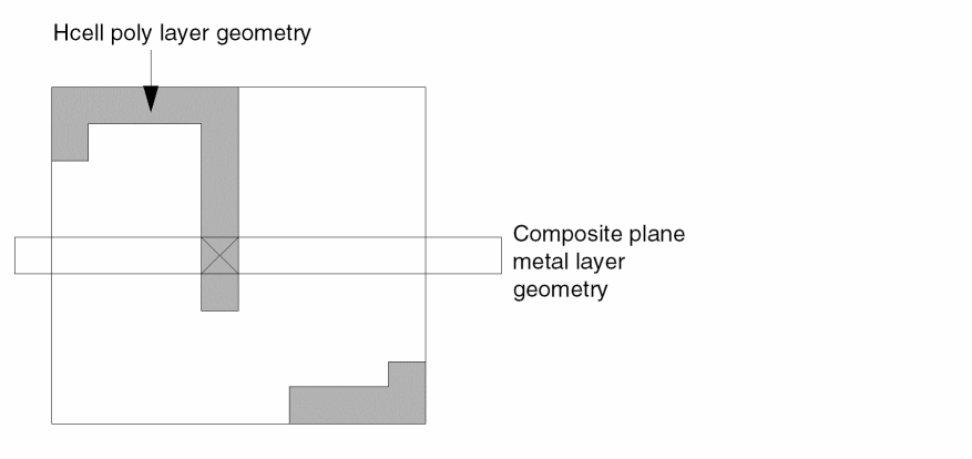
- Geometries from the composite plane or other Hcells can overlap Hcells (Hcell box), but they cannot delete, add, or modify any devices within the Hcell, except by the BASE-LAYER command. In cases where such devices are formed by these overlapping geometries, Dracula flags them as “EXTRA CELL TO COMPOSITE” devices.
Automatically Selecting HLVS Hcells
Dracula can automatically select HLVS Hcells, as it does for HDRC. However, in HLVS you must cross reference layout and schematic cells. If layout cell names and their equivalent schematic representations are different, Dracula uses a cross-reference table to match them.
The ref-filename lists layout cell names with their corresponding schematic cell names. The format of the reference file is the same as for the HCELL-FILE command. Each line contains two names with blanks as delimiters. The first name is the layout cell name, and the second is the corresponding schematic cell name.
When selecting Hcells, Dracula starts with the cells listed in the reference file. First, Dracula selects Hcells according to the same criteria it uses to select HDRC Hcells. Then Dracula drops all Hcells not listed in the schematic netlist.
To run HLVS using automatic Hcell selection, follow these steps:
-
To create the file jxauto.com, run PDRACULA.
%PDRACULA
%/get rulefile.rul n auto
%/fin
-
To generate an Hcell table, execute jxauto.com. The HCELL-FILE file specifies the file name for Hcell table.
%jxauto.com > jxauto.log
-
To examine the validity of the newly generated Hcells, run LOGLVS.
%LOGLVS
: CELL/AUTO HCELL-FILE
: .
: X
-
To create the final jxrun.com, run PDRACULA.
%PDRACULA
-
To run HLVS, execute jxrun.com.
%jxrun.com
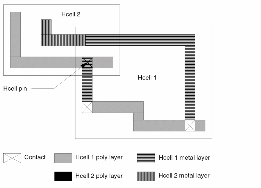
Hcell Pins
Hcell external connections to other Hcells on the composite are allowed only at the pins (also called terminals). In schematics, this is the only way to designate terminal connections. You can identify a pin in the netlist subcircuit by declaring the name as an I/O pin. You can use text to identify the node of a pin in the layout. In the Hcell layout, place text on a node where the Hcell connects with another Hcell geometry or with a composite geometry.
An Hcell can be a dummy cell with only its I/O pins and power pins digitized and assigned text. A corresponding netlist subcircuit with its I/O pins specified allows an HLVS composite mode run to check the correspondence of the layout block pins (with unspecified internal circuits) against the pins of the corresponding subcircuit in the netlist. For more information about dummy cells, refer to the BLACKBOX-FILE command in
Interconnect between Hcells does not have to be at the Hcell boundary. You can locate pins within the Hcell and connect them using a pin of an overlapping Hcell or to an overlapping geometry from the composite plane.
Hcell Text (Pin Names)
HLVS, like LVS, identifies external pins of a circuit by using your text information. HLVS has texting requirements beyond those of flat mode LVS. To run a cell mode HLVS, text a minimum number of pins in the Hcell layout in addition to a minimum number of pins in the composite plane layout.
For cell mode HLVS, you must text power, ground, and at least one signal node for each independent circuit within the Hcell. An independent circuit is a net consisting of the set of all connections and components that have direct or indirect (that is, through a device) connections among themselves. For example, if two D flip-flops have a pin on the D input, a pin on their Q output, and no other connections, the two are independent circuits. But if the D input of one is tied to the Q output of the other, they are part of the same independent circuit.
For a cell mode HLVS run, use the GEN-TEXT command to eliminate manual texting of Hcell pins. GEN-TEXT generates complete Hcell pin text starting from the minimal text information required for a cell mode HLVS run and combines that with the pin names found in the netlist. For more information about texting Hcells, refer to the
Adding to Text
You can add text for the flat or composite planes with either or both of the following methods:
- Read text from the input database by specifying the layer containing it in the TEXT= layer command in the Input-Layer block.
- Read text and coordinates from the file listed in the EDTEXT command.
You can provide Hcell text with either or both of the following methods:
- Read text from the input database as specified in the layers defined by CTEXT= layer commands in the Input-Layer block.
- Read text and text coordinates from the file specified in the HEDTEXT- file command. You can create this file with a text editor or the GEN-TEXT command. For details, refer to the GEN-TEXT command in Chapter 12, “Input-Layer Block Commands.”
In a composite mode HLVS run, you must assign text to all Hcell pins. An easy way to add text is first to provide minimum texting for the composite plane pins and for the Hcell pins. You can do this by adding text in the original database or by generating a HEDTEXT file. Next, run a cell mode HLVS with GEN-TEXT enabled, which creates a new HEDTEXT file with all the Hcell pin text included. Finally, run a composite mode HLVS using the HEDTEXT file created by GEN-TEXT.
Pin Text
You can create an additional physical layer for text layers so you can use logical operations on them. When you use the PIN-TEXT-LAYER command in the Input Layer block of the rule file, Dracula creates a square on the specified layer surrounding the text origins for each text layer on the composite plane.
The default size for the square is 2x2 database units. You can specify any size for the square; however, if the size is an odd number, the text origin is not in the center because text origins must be located on an integer.
Example
The following example uses the PIN-TEXT-LAYER command in the Input-Layer block of a rule file.
*DESCRIPTION
.........
*END
*INPUT-LAYER
PIN-TEXT-LAYER = PINLAY
POLY = 5 CTEXT= 21
......
CONNECT-LAY = NSUB PWELL PSD NSD POLY METAL
*END
*OPERATION
; Logical Operations
;-------------------
AND PINLAY METAL LAY1
.........
; Perform Layer Interconnection
;------------------------------
STAMP PINLAY BY LAY1
.............
*END
Masking Hcells with Black Boxes
In composite mode, you can mask an Hcell with a “black box.” A black box is a pin geometry-only replacement of an Hcell master whose original definition either does not exist or should be ignored. Define a black box when
- The Hcell master is another company’s proprietary design and you have only the pin information for the Hcell.
- The Hcell master has been verified by other means and you are not concerned about cell-to-master interactions other than the composite-to-cell pin connectivity. This use is similar to the FRAME BY command, except that you provide the frame.
Before defining a black box, you must be aware that HLVS cannot check a black box for violations such as connections from composite-to-cell internal nodes. Also, if the black box is specified incorrectly, it can cause serious problems. Dracula might overlook some LVS errors or report false mismatch violations.
Use a black box file to define black boxes. The BLACKBOX-FILE command in the Description block identifies the file name. Each line in the black box file generates a pin geometry in the replacement Hcell master. Each line must list the following items:
- The text name
- The x,y coordinates where the pin geometry is to be centered
- The attached layer
- The name of the Hcell
Optionally, you can use width (w) and height (h) specifications to define the shape of the pin.
For more information about the black box file, refer to “BLACKBOX-FILE”.
Hcells and the BASE-LAYER
HLVS lets Hcells overlap and connect at Hcell pins in the overlapping area. The composite plane can also have geometries that overlap or cross Hcells and connect at Hcell pins. The netlist must reflect this connectivity to avoid discrepancy errors. Dracula automatically checks devices created by composite plane geometries overlapping Hcells and lists them in the HLVS discrepancy report.
The BASE-LAYER command allows geometries digitized in the composite plane to be considered Hcell geometries. These geometries form devices and indicate connectivity. In a limited sense, the BASE-LAYER command handles geometries that are not identical for different placements. Geometries that are the same for each placement move into the cell. Unique portions of the geometries stay in composite level.
This is important for some gate array types of layouts, where composite plane layers (the base-layers) provide a set of symmetric geometries overlaid by Hcells that parameterize the semicustom circuit with transistors, contacts, and other connections. For details about this functionality, refer to the BASE-LAYER command description in
Hcell Frames
You can specify Hcell frames for composite mode HLVS when you use the HCELL or HCELL-FILE commands. The frame is a rectangular area in the Hcell that tells Dracula to discard the geometry sections in it, leaving only the geometry sections in the area between the frame and Hcell box. This area along the boundary of the Hcell remains available to let composite mode HLVS determine the external pin connections of the Hcell by matching the geometries being connected and their text (pin name).
GEN-TEXT warns you of pins that are located in the empty region of the frame that cannot be assigned text. You must make the frame border large enough to include these pins. Otherwise, Dracula drops the text. When using Hcell frames and GEN-TEXT, be sure to put text in the proper places, as explained in the “GEN-TEXT Commands” section.
Wire Types
The concept of wire types is similar to virtual wires in flat Dracula except that it provides more flexibility as needed by the hierarchical environment. You can specify MustJoin wire types for pins by adding a semicolon (;) and a number after the signal name or pin text. For example, Q;25. There are two kinds of wire types: MustJoin and Internally-Wired.
MustJoin Wire Type
Pins with the same text name and different wire types are MustJoin wire types. These pins are assumed to be the same node even though they are not connected within their level (Hcell or composite plane). They are joined at some higher level. If the MustJoin wire type pins are in an Hcell, a composite mode HLVS verifies a connection between the two pins at the composite level. This MustJoin convention is equivalent to the Virtual Wires convention (Q: and Q:), but it is more general and precise in the hierarchical environment. For this reason, do not use virtual wires (:) for cell mode texts.
Internally-Wired Wire Type
Dracula considers pins with the same text name and the same wire type, such as Q;3 and Q;3, to be internally wired. This means that these wires must be connected within the Hcell in which they are found. A cell mode HLVS run verifies these connections. These pins are particularly important when you use a frame in composite mode to eliminate the layout within a cell, leaving only the pins. If you make two or more external connections to the same geometry at two different places, and if a frame cuts the geometry in the cell, you must label both connect-points of the geometry with an internally-wired wire type. Use a number between 1 and 3000 to name the wire type. Composite mode HLVS then knows that these two physically disjointed connections correspond to the same pin. Note that a wire name with no type (for example, Q) corresponds to a name with wire type of type “0 (zero)” (for example, Q;0).
When Dracula assigns a wire-type number, HLVS treats virtual wires as MustJoin wire types. Dracula accepts both wire type conventions and virtual wires for composite or flat data. Cell data must use the semicolon (;) convention.
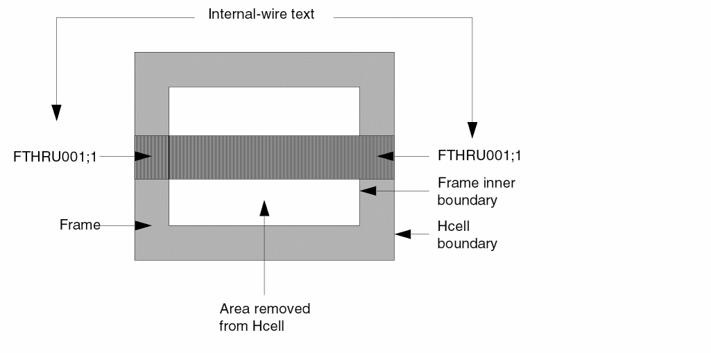
Feedthroughs
Feedthroughs are interconnects that run through an Hcell without making a connection to any device in the Hcell. They route signals through a cell. Feedthroughs do not have a counterpart in the netlist Hcells; rather, they are part of the composite-plane interconnect. When feedthroughs exist, Dracula requires that you identify them in the Hcell layout by texting them with a label starting with FTHRU followed by one or more digits. This label tells HLVS to ignore the feedthrough in a cell mode HLVS and to use it to connect nodes in a composite mode HLVS. The GEN-TEXT operation can identify feedthroughs and text them.
GEN-TEXT Commands
The GEN-TEXT operation reduces the amount of effort needed to text all Hcell pins as required for a composite mode HLVS operation. GEN-TEXT relies on HLVS to provide texting information for pins not assigned text. Hcells must have the required minimum texting so that a cell mode HLVS can run. Cell mode HLVS with GEN-TEXT enabled extracts text information from the netlist subcircuits and generates an HEDTEXT file containing all Hcell pin text. Subsequent HLVS runs can use this HEDTEXT file as input.
Use GEN-TEXT to save effort in texting Hcell pins, and, if the cell mode run completes successfully, ensures there are no differences between the names in the layout text and the corresponding netlist signal.
Running GEN-TEXT in flat mode is the same as running GEN-TEXT in cell mode with one Hcell. Because you can run GEN-TEXT in any mode, integrate the resulting text files from separate runs into one file for the final composite check.
Running GEN-TEXT in composite mode lets you run a job in composite mode more than once to verify the entire chip. For example, an Hcell (cell-A) at the chip level (cell-chip) might be so large that a flat or cell mode run might not process the LVS GEN-TEXT for cell-A. If you can identify the cells you place inside of cell-A as Hcells, then you can
- Run cell mode GEN-TEXT for cells inside of cell-A.
- Run composite mode GEN-TEXT on cell-A. Combine your GEN-TEXT file with the text created in the separate runs.
- Combine the text of all Hcells in cell-chip.
- Run composite mode LVS on cell-chip.
You can use the following commands to control the GEN-TEXT operation.
Description Block Commands
GEN-TEXT-FILE = file-name
This command starts the GEN-TEXT operation in HLVS. The file-name is the text file to be generated.
GEN-TEXT-FLTNODE = YES/NO
This command specifies whether GEN-TEXT should automatically identify feedthroughs and label them with FTHRUxxxx text labels.
GEN-TEXT-FRAME = xxx MICRONS
This command simulates a frame corresponding to Hcell Frames to be used in a composite mode HLVS. This simulated frame allows GEN-TEXT to determine whether errors exist in attempting to create text within the frame area.
GEN-TEXT-WIRE = YES/NO
This command finds pin nodes that must be labeled as Internally-Wired because they have been split by a frame (GEN-TEXT-FRAME command) and labels them with an Internally-Wired wire type label.
Input-Layer Block Command
GEN-TEXT-LAYER = layer...
This command specifies layers to be assigned text.
Using Frames with GEN-TEXT
You do not need a frame to run HLVS, but you can use a frame to reduce execution time. To specify a FRAME option on Hcells in a composite mode HLVS and to use GEN-TEXT to generate text, follow these steps:
- Enable GEN-TEXT with the GEN-TEXT-FILE command.
- Use GEN-TEXT-FRAME (FRAME BY in the Hcell table overwrites the GEN-TEXT-FRAME in the associated Hcell).
- Use GEN-TEXT-WIRE = YES.
- If Hcells have feedthroughs, use GEN-TEXT-FLTNODE = YES.
- Ensure that none of the Hcell commands or HCELL-FILE statements specify the FRAME option during the cell mode run.
- Provide a HEDTEXT command pointing to the file created by the GEN-TEXT-FILE command during the cell mode run.
- Make all frames specified in Hcell commands or HCELL-FILE statements have the same size as the frame specified in the GEN-TEXT-FRAME command. (Cell mode and composite mode runs can share the HCELL-FILE statements.)
These steps guarantee that if a frame splits a pin assigned text or a feedthrough with two connect locations, Dracula correctly assigns text to the pin or feedthrough using an Internally-Wired wire type. For details, refer to the
Example of GEN-TEXT Commands
The following file is a section of the Description and Input-Layer blocks in a rules file that uses GEN-TEXT with floating-node and wire type options and an 8-micron frame.
;
*DESCRIPTION
;
;    HEDTEXT file produced is gen.txt
;
  GEN-TEXT-FILE = gen.txt
;
;    Use 8 micron frame.
;
  GEN-TEXT-FRAME = 8 microns
;
;    Generate feedthrough text labels
;
  GEN-TEXT-FLTNODE = yes
;
;    Distinguish wire types
;
  GEN-TEXT-WIRE = yes
;
*END
*INPUT-LAYER
;
;    Specify layers for GEN-TEXT to text.
;
  GEN-TEXT-LAYER =  psub  nwell  poly  metal
HLVS Error Types
LVS flags overhang geometries of two different cells, or different internal nodes of the same cell, that are connected as potential embedded errors rather than true errors.
Sample HLVS Input Rules File
This is a sample rules file for a PWELL CMOS standard cell.
*DESCRIPTION
CHECK-MODE = composite ; $$$ new $$$
HCELL-FILE = hcell.tab ; $$$ new $$$
PRIMARY = chip
SYSTEM = gds2
INDISK = lvs.db
OUTDISK = lvsout
SCALE = .001 mic
RESOLUTION = .05 mic
PRINTFILE = lvsprt
MODE = exec now
PROGRAM-DIR = /dracula
schematic = LVSLOGIC
*END
;
*INPUT-LAYER
nplus=2
pplus=3
poly =4
met1=6  text=58     ; composite text
poly=23 CTEXT = 18  ; Hcell text $$$ new $$$
met1=24 CTEXT = 20  ; Hcell text $$$ new $$$
cont=5
pwell=1
SUBSTRATE=bulk 54
;
CONNECT-LAYER = nsub pwell psrcdrn nsrcdrn poly met1
;
*END
;
*OPERATION
HEDTEXT = pinnames.txts ; $$$ new $$$
NOT bulk pwell nsub
AND poly nplus ngate
AND poly pplus pgate
NOT nplus ngate nsrcdrn
NOT nplus pgate psrcdrn
;
CONNECT met1 nsrcdrn    BY cont
CONNECT met1 poly       BY cont
CONNECT met1 psrcdrn    BY cont
CONNECT psrcdrn pwell   BY pwell
CONNECT nsrcdrn nsub    BY nsub
;
ELEMENT MOS[N] ngate poly nsrcdrn pwell
ELEMENT MOS[P] pgate poly pscrdrn nsub
;
LVSCHK
*END
Inherited Connections for LVS in Dracula Verification
Inherited connections is an extension to the connectivity model that allows you to create global signals and override their names for selected branches of the design hierarchy. This flexibility allows you to use
- Multiple power supplies in a design
- Overridable substrate connections
- Parameterized power and ground symbols
To learn about connectivity and naming conventions for inherited connections and how to add and edit net expressions in a schematic or symbol cellview, refer to the "Inherited Connections" sections in chapter 2 of the Virtuoso Schematic Composer User Guide.
Once parameters for a net are specified in the top (upper) level of a schematic or symbol cellview of a design, the instances ( in the lower level) inherit the same connectivity from the parameters specified on the top level.
Example
If you have a logic that includes two inverter instances, I1 and I2, then to verify if the netlist in that design has inherited connectivity, follow these steps below.
- Select the consistent logic (schematic) and layout data. You can run CDLOUT on one logic (schematic view) and correctly pick the corresponding layout.
- Run CDLOUT on your logic data to get the needed netlist.
-
Check to see if in the top cell in your netlist you have two same instance, for example
I1andI2that have been assigned different POWER and GROUND connections on the top level. For example,gndandvddfor one instancea_gndandN33Vfor another instance This means that the two same instanceI1andI2have followed the "inherited connections" rule and have inherited different POWER and GROUND assignments from the top level respectively. -
Run LVS for the above netlist and its corresponding stream.
You will get a
*.DATfile, for example6PADS.DATfile. When you view this.DATfile, you see for example,
GND 1 G 0
VDD 2 P 0
N33V 3 O 0
A_GND 4 O 0
OUT1 5 O 0
INI 6 I 0
Check to see if the GND (PAD 1)and A_GND (PAD 4) are assigned to the same instance respectively.
-
Check the LVSLOGIC file and view its contents and you see that there are two MOS elements (one for
I1and another forI2) in the instance being parsed by LOGLVS. And, their source node ( connected to GROUND) is assignedPAD1andPAD4respectively. This means that although this instance did not specify certain parameters for the POWER and GROUD originally, once the parameters are specified in the top (upper) level, the instances (in the lower level) are also inherited from the parameter specified on the top level.
Return to top