7
Extracting Electrical Parameters (LPE)
This chapter focuses on the following topics for LPE in Dracula:
- “LPE Overview”
- “LPE Flow Diagram (continued)”
- “Flexible LPE”
- “Selective LPE”
- “LPE Examples”
- “Hierarchical LPE”
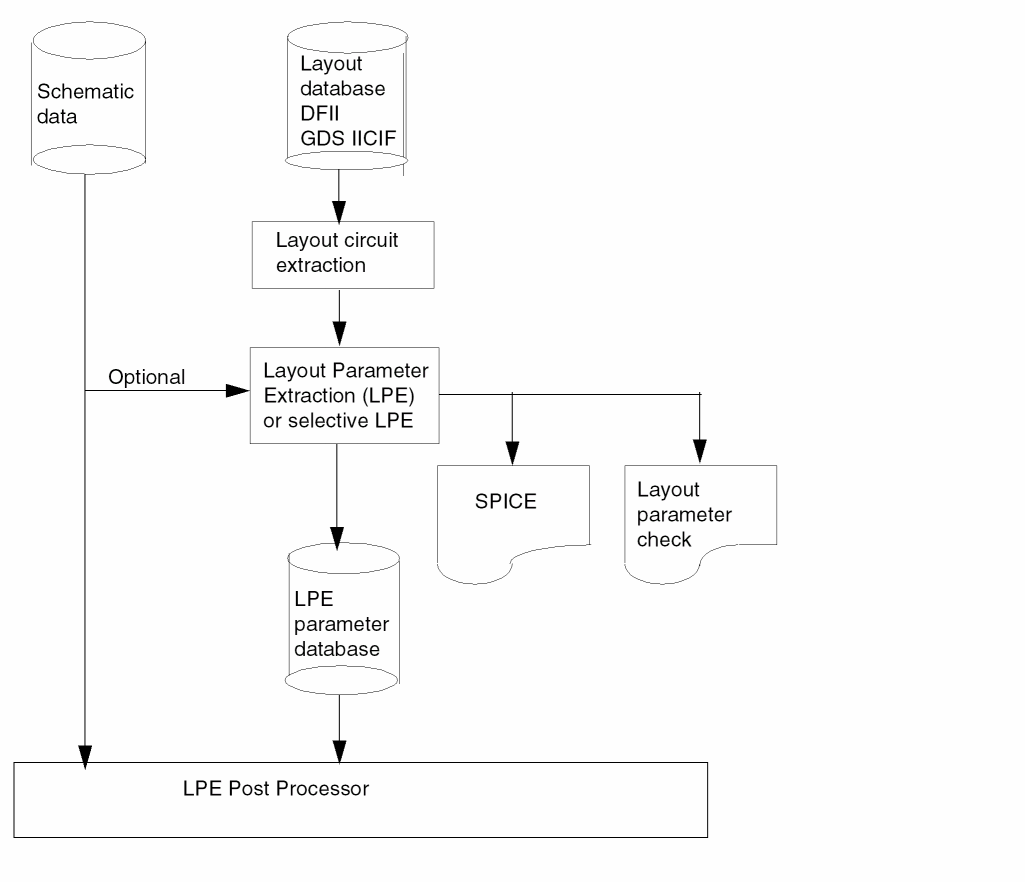
LPE Overview
Using an integrated circuit (IC) layout, Layout Parameter Extraction (LPE) computes and extracts key electrical parameters, such as
- Node parasitic capacitances
- Defined resistors
- Diode areas and perimeters
- Bipolar device sizes
- Transistor gate sizes
You can use these extracted parameters in Layout vs. Schematic (LVS) consistency checking, in circuit and logic simulations, and in timing verification.
IC designers use circuit and logic simulations to predict product performance. You usually run simulations with estimated device sizes and loadings, and the simulations are not necessarily accurate reflections of layout performance. Substantial tolerances and safety margins are required to avoid design discrepancies. LPE gives you more precise values for physical devices and loadings so that simulations more accurately reflect layout performance.
LPE creates both the layout parameter database and the link between layout and schematic compiled by the Layout Versus Schematic Network Compiler (LOGLVS). For information about LOGLVS, refer to
You can use LPE as a standalone system or with the Design Rules Checker (DRC), Electrical Rules Checker (ERC), or LVS. LPE extracts the width and length of a MOS transistor, the areas and perimeters of a bipolar transistor, the areas and perimeters of a diode (source/drain diffusion), the capacitances of a node (with cross-coupling), and drawn resistance.
You can run LPE with hierarchical Dracula. For more information, refer to the
In batch mode, LPE reports in a SPICE-compatible format. You can submit the SPICE listing for circuit simulation with only minor editing, such as adding model information. You can select the following LPE reports:
- Program-assigned node/device names/numbers with cross-references to layout labels
- Program-assigned node/device names/numbers with cross-references to schematic I/O’s and designators
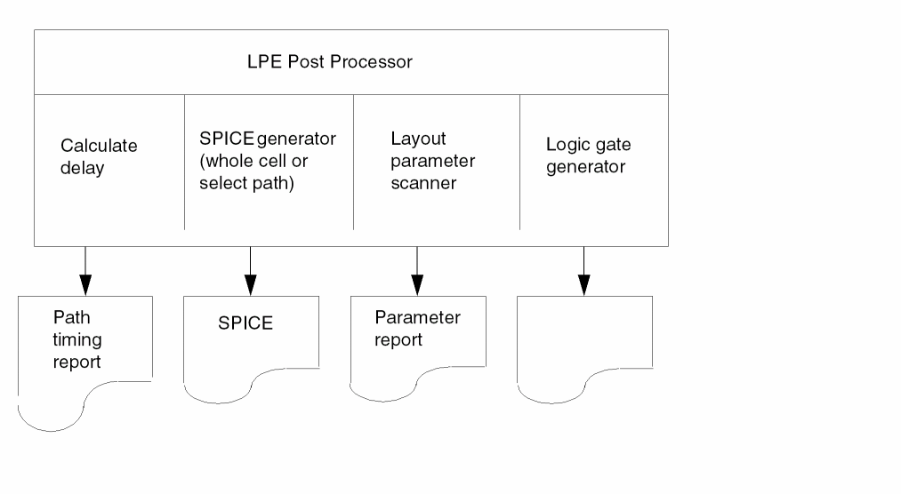
LPEPRO performs the following functions interactively:
- Probes circuit parameters with your relational thresholds
- Manipulates circuit parameters with your formulas
- Selects your circuit path and outputs all devices along the path in SPICE format so that you can do simulation selectively
- Reproduces the logic gate formation from the layout
- Locates the longest and shortest paths
- Automatically adopts all element types, model names, parameters, units, and other descriptions specified in the LPE rules file
LPE follows the standard Dracula layout texting procedure. If you do not want to backannotate the circuit schematic with the extracted parameters, label only power and ground nodes. For a layout-to-schematic comparison, label the I/O’s.
LPEQRY lets you extract devices and parameters associated with specified nets. It is both unnecessary and time consuming to run parameter extraction of all nets on a large, complex chip when you are interested in analysis of only the critical path.
You must compile your schematics with the LOGLVS Network Compiler. LOGLVS accepts HSPICE, SPICE2, and Verilog schematic descriptions.
The following figure shows the relationship between LPE and LPEPRO.
LPE Flow Diagram
LPE Flow Diagram (continued)
Extracting SPICE Parameters
The following sections describe standard SPICE parameters and user-specified parameters. LPE extracts for MOS, parasitic diodes, parasitic capacitors, element resistors, and bipolar devices.
MOS Transistors
This section describes how Dracula calculates MOS transistor channel width and length in the graphics database.
Calculations Without Adjustments
WEFFECT=0 or CORNER=0 (Default)
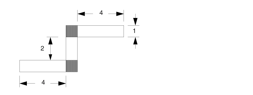
The transistor widths to the source and drain are the MOS transistor gate perimeters that touch or overlap the diffusion area. The average of the transistor widths at source and drain is the width for the gate area. The transistor length is the ratio of the total gate area to the average of the widths at source and drain.
LPE extracts parameters from the drawn geometry. If you can estimate the actual size of a transistor, you must undersize or oversize the gate area to the proper scale before parameter extraction. LPE does not automatically extract the gate to the substrate capacitance. You must define the extraction using the PARASITIC CAP command. You can use the ATTACH command to extract the area and perimeter of the diffusion and attach this information onto the MOS device. The following figure shows the default method for measuring width and length without adjustment.
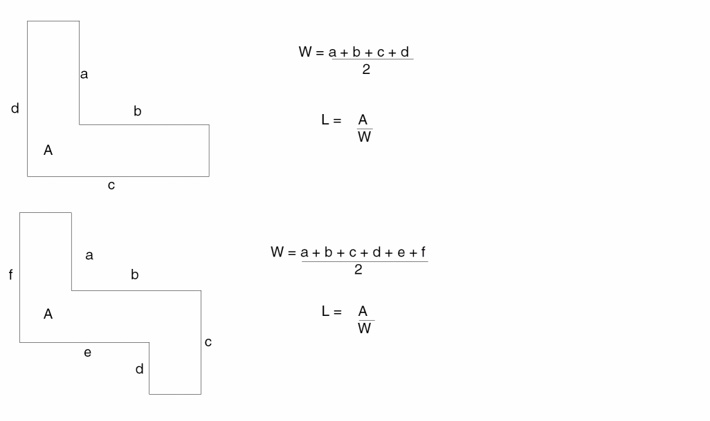
Where a+b+c+d+e+f represents the perimeter of the active gate area.
To extract MOS source/drain area, perimeter, and output as AS, AD, PS, and PD in SPICE, use the LEXTRACT and ATTACH commands. The following example illustrates this.
*DESCRIPTION

...
PARSET TEST AREA PERI
...
*END
...
*OPERATION
...
ELEMENT MOS[N] NCHNL METAL DIFFN OVPWELL;
ELEMENT MOS[P] PCHNL METAL DIFFP NSUB   ;
...
LEXTRACT TEST DIFFN BY NODE PDIFFN
LEXTRACT TEST DIFFP BY NODE PDIFFP
ATTACH MOS[N] PDIFFN &
ATTACH MOS[P] PDIFFP

...
LPECHK
LPESELECT[S] MOS &
...
Calculations With WEFFECT or CORNER Specified
You can specify a positive or negative value for WEFFECT in the LVSCHK or LPECHK command. The same restriction is true for CORNER in the LPESELECT command. When you encounter turns or corners, Dracula calculates the MOS channel width/length as follows:
For a pulldown device where W>L, each 15-degree turn in the transistor channel adds or subtracts 1/6 of WEFFECT/CORNER times the length, L, from the transistor default width, W. For a load device (L≥W), the channel length is modified. The following examples illustrate these calculations (CORNER can be substituted for WEFFECT).
-
For a pulldown device (L is unmodified)
W{actual} = W{init} - (WEFFECT * I *L) ; if W{init} is greater than L
where
W{actual} = the actual width of the gate
W{init} = the initial width of the gate. This is always calculated by Dracula.
WEFFECT = a compensation coefficient you supply to Dracula to correctly calculate the actual width/length of a transistor gate.
I = the total of a device’s internal angles (in units of 90 degrees)
L = the length of the gate which is equal to the total area of the gate divided by the initial width of the gate (e.g. Area/W{init}) -
For a load device (W is unmodified)
L{actua}l = L{init} - (WEFFECT * I *W) ; if L{init} ≥ W
where
L{actual} = the actual length of the gate
L{init} = the length of the gate which is equal to the total area of the gate divided by the width of the gate (e.g. Area/W)
WEFFECT = a compensation coefficient you supply to Dracula to correctly calculate the actual width/length of a transistor gate.
I = the total of a device's internal angles (in units of 90 degrees, with each internal angle rounded to the nearest 15 degrees)
W = the width of the gate. This is always calculated for you by Dracula. -
For parallel MOS pulldown transistors (of the same type):
Example 1
I/90 = 2 [90 + 90 = 180 degrees]
For a pulldown device: WEFFECT= 0.5, W = 12 L = 1, and Wactual = 11
For a load device: WEFFECT= 0.5, W = 1 L = 12, and Lactual = 11
Example 2
I/90 = 1 [45 + 45 = 90 degrees]
For a pulldown device: WEFFECT = 0.0, W = 16 L = 3.31, and Wactual = 16 where WEFFECT = CORNER.
For another pulldown device: WEFFECT = 1.0, W = 16 L = 3.31, and Wactual = 12.69
Parasitic Diode Parameters
LPE extracts the parameters of a positive-negative (P-N) junction diode. The source/drain diffusion area and the substrate/well on which it is diffused make up the two diode terminals. The polarities of the terminals are positive if P-doped and negative if N-doped.
You can extract as many as six types of diode parameters: A1, P1, A2, P2, A3, and P3. The choice of A2,P2 and A3,P3 depends on whether you specify the second and third argument layers in the PARASITIC DIO command. These two layers cannot overlap when both are needed to define a diode. For more information about the PARASITIC DIO or DIODESEQ commands, refer to the “Description Block Commands” and “Operation Block Commands” chapters.
To reduce the number of diodes for simulation, LPE lumps the parameters of the same diode type at the same node into one parameter before reporting them.
Parasitic Capacitor Parameters
LPE defines most kinds of capacitance in any process technology with combinations of logical and sizing commands. After the connections of a circuit are established with CONNECT commands, the node numbers automatically pass from the first argument layer to the output layer on each logical AND/NOT command. The two layers that define a parasitic capacitor determine the connections between the two terminals of a capacitor.
LPE-extracted capacitance is always coupled from one node to another and skips the capacitors with both terminals at the same node. LPE reports the combined load capacitances of a node in lump sum format as the default unless you specify otherwise with the LPESELECT[C] command.
In addition to capacitance values, the parameter database includes the area and perimeter of the capacitor. You compute capacitance values by specifying the area and perimeter coefficients in the ATTRIBUTE CAP command. For details about the ATTRIBUTE CAP command, refer to “ATTRIBUTE CAP”.
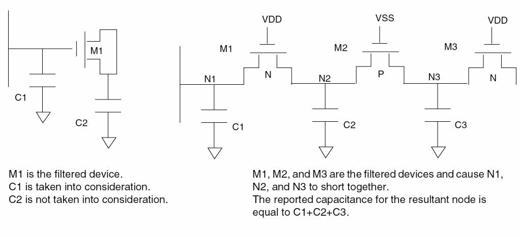
Device Filtering
With device filtering on, if a filtered device has one terminal connected to one net of the circuit after filtering, the capacitance of the filtered device, which is related to the net, is taken into consideration. All parasitic capacitance related to the merged nodes is added to the resultant node. The following illustration shows how LPE handles filtered devices.
Element Resistor Parameters
To define the resistor device layer and terminals, use the ELEMENT RES command. To assign sheet resistance for a resistor device defined by the ELEMENT RES command, use the PARAMETER RES command.
To define effective width, device size extraction uses the device layer where it touches terminals W1 and W2. Device size extraction uses area and effective width to compute the effective length of the resistor. You must properly size or logically create the terminal layer to ensure the correct resistance value.
To specify the scale factor of unit values to resistor value, use the UNIT command in the Description block. If you do not specify the unit name, LPE lists the parameter in natural units.
Example of a Typical Resistor
This example shows the equation for a typical resistor.
*DESCRIPTION
.
UNIT = capacitance,pf resistance,k
.
*END
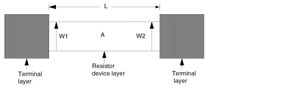
W = (W1 + W2) / 2 and L = A / W
W is the effective width of the resistor. L is the effective length of the resistor. A is the total area of the resistor device layer.
Resistance, R = (value) * ( L / W )
The value is the sheet resistance per square specified in the PARAMETER RES command.
This equation is applicable for a bent resistor with corners. The area adjusts the resistor length, which becomes a center line length.
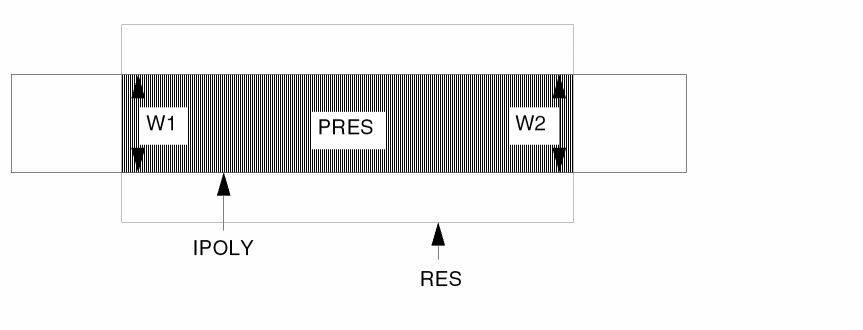
Example of a Typical Polysilicon Resistor
This is an example of how you can use an extra digitized layer to identify an element. In this example, poly, the conductor layer created from the ipoly layer (complete polysilicon layer) and the res layer, acts as the resistor terminal. To extract a resistance value, you must specify the PARAMETER command.
The ipoly layer is polysilicon, and the res layer is a digitized resistor layer.
*DESCRIPTION
.
UNIT = resistance,k
.
*END
*OPERATION
.
AND ipoly res pres    ; Device layer
NOT ipoly pres poly   ; Poly-si interconnect &
                      ; resistor terminals
.
ELEMENT RES[P] pres poly
PARAMETER RES[P] 200
.
LPECHK
LPESELECT res &
.
*END
Example of Diffusion Resistors
In this example, the diff layer is the complete diffusion layer, the dres layer is the diffusion resistor, and the cont layer is the metal-diffusion contact.
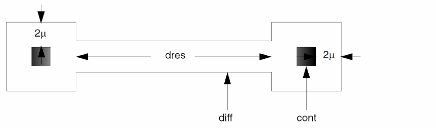
Note that the diff layer is a logical and/or select-generated layer. You must resize the cont layer to generate the “touch” of the device layer, dres.
*DESCRIPTION
.
UNIT = resistance, ohm   ;In this case, the UNIT
                         ;command is not necessary
.
*END
*OPERATION
.
SIZE cont BY 2 ocont     ;Oversize CONT
NOT diff ocont dres      ;Device layer for resistor
NOT diff dres srcdrn     ;Source drain layer without
                         ;contact terminals
.
CONNECT metal srcdrn BY cont
.
.
ELEMENT RES[D] dres srcdrn
PARAMETER RES[D] 15
.
LPECHK
LPESELECT res &
.
*END
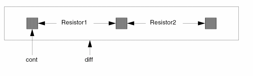
For more than two terminal-drawn resistors (Y-shaped, T-shaped, and so forth), you must generate an intermediate node (contact terminal). If you do not generate an intermediate node, you get an undefined resistor device (?RES).
The following figure shows diffusion resistors in a series where the resistor bodies are not separated by contacts.
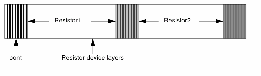
You must transform the process shown above by SIZE, LOGICAL, or SELECT operations. The following figure shows how to correct the extraction of the two resistors.
Examples of Problem Resistors
In the examples in the preceding section, the resistor terminals precisely touched the resistor device layer so that W1 and W2 measured the same. If the resistor terminals do not precisely touch the device layer, the calculated W and L might be slightly different.
Example of Width Not Measured Precisely
The following example shows where resistors width is not measured precisely.
Example of Length Not Measured Precisely
This figure shows an example of resistors where length is not measured precisely.
LPE and LVS extract resistor devices and device sizes. The same resistor equation for W and L applies, but the extracted resistor device sizes vary depending on the interrelationship of the resistor device layer and the resistor terminals (precise touch expected).
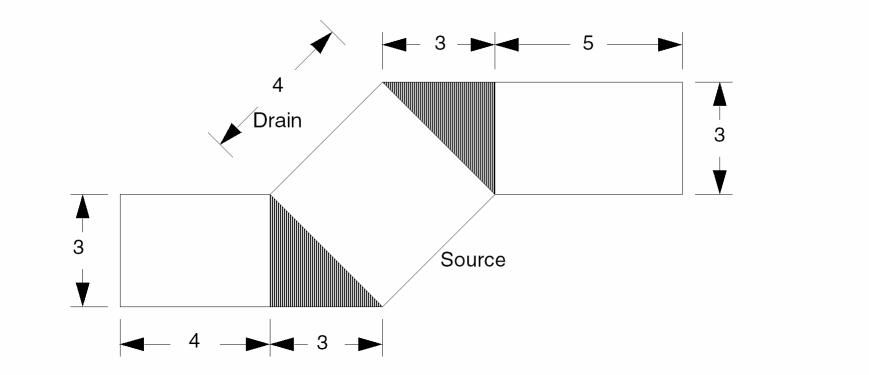
Bipolar Transistor Area and Perimeter
This section shows you how to extract and measure parameters for bipolar transistors. LPE extracts bipolar device parameters and creates a CDL/SPICE netlist. The DEVTAG and LEXTRACT operation commands handle bipolar devices. With these commands, you can extract parameters from other associated layers or geometries of the same device (multiple collector or emitter bipolar devices). For more information about these commands, refer to
Using Bipolar LPE
- To define bipolar devices, use the ELEMENT BJT command.
- To tag device numbers to layers that are not device layers but from which you want to extract parameters, use the DEVTAG command.
-
To specify the parameters (area and/or perimeter) you want to extract and the layers from which you want to extract them, use the LEXTRACT command.
The program supports the following parameters for bipolar transistors:
If you do not specify the LEXTRACT command, LPE extracts only area and perimeter from the device layer you specify in the ELEMENT BJT command. The default assumes the device layer is the emitter; the netlist reports the area and perimeter as “EA” and “EP.” If you want the area and perimeter of a terminal other than the device layer as output, use the DEVTAG and LEXTRACT commands. - To define the parameter set (area and/or perimeter) to be extracted, use the PARSET command.
- To specify model names for bipolar transistors in the Description block, use the MODEL command.
- To backannotate to schematics and to create the CDL/SPICE netlist, use the LPECHK and LPESELECT commands.
Example of Vertical npn
In this example, Dracula extracts the emitter area and the perimeter by default. The nemit layer is the device layer, buried is the device collector terminal, and base is the device base terminal. The nemit layer is also the device emitter terminal.
Example of Vertical pnp
In this example, Dracula extracts emitter areas, base areas, and perimeters and includes them in the bjtvp parameter file. The pemit layer is the device layer, psub is the device collector terminal, epi is the device base terminal, and pemit is the device emitter terminal.
Example of Lateral pnp with Possible Multiple Collector
In this example, Dracula extracts the emitter areas, collector areas, and perimeters and includes them in the bjtlp parameter file. To tag the device numbers, Dracula must go back to emit (the true emitter) through ovemit (the intermediate layer oversized emitter). Dracula performs extraction through the temit file, which has device numbers linked by the DEVTAG command. No tagging is necessary for the coll layer because it is the device layer.
In this example, coll is the device layer and the device collector terminal, buried is the device base terminal, and ovemit is the device oversized emitter terminal. The emit layer is the true size emitter; emit1 and temit are files created by DEVTAG that contain device number information.
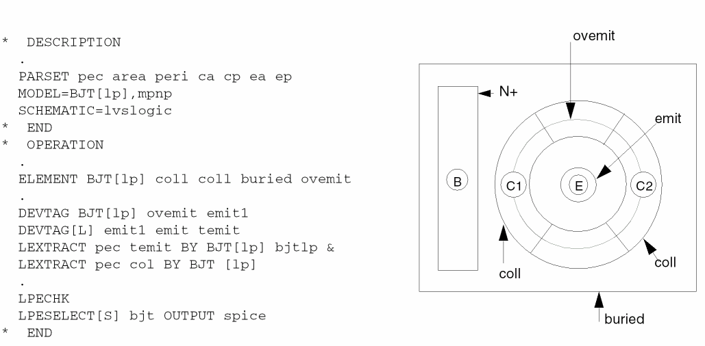
Remember that the dollar sign ($) is a SPICE comment delimiter.
Q1  out1   in1  gnd  npn   $ EA=100  EP=40.
Q2  vcc    xfr1 out6 vpnp  $ BA=900  BP=120  EA=100  EP=40
Q3  cout1  in3  vcc  mpnp  $ CA=400  CP=80  EA=400  EP=80
Q4  cout2  in3  vcc  mpnp  $ CA=400  CP=80  EA=400  EP=80
Flexible LPE
LPE supports standard CDL or SPICE parameters for devices. Flexible LPE lets you define parameters and extract them by specifying your equation. Flexible LPE supports all CDL or SPICE parameters (reserved parameter keywords), and you can output these parameters with the LPESELECT command in the SPICE file generated by LPE.
Flexible LPE has three types of parameters: geometric primitives, reserved parameter keywords, and user-defined parameters.
Geometric Primitives
The primitives defined below refer to the relation of a layer to itself and to other layers. To extract values from the relation of the specified layers to layer-a, use the LEXTRACT and PARSET commands.
Reserved Parameter Keywords
Reserved parameter keywords are for parameter values for devices you usually use for CDL or SPICE simulations. If you specify LEXTRACT for a device, you must specify an equation for each of these parameters in the PARSET command list. For more information about the PARSET list, refer to
|
Fringe capacitance attribute used for piece-wise fringe capacitance |
|
User-Defined Parameters
Any names you define can have a maximum of four characters. The first character must be from A to Z. The remaining characters can be A-Z and 0-9. If you specify an LEXTRACT command for a device, you must specify an EQUATION command for each parameter in the PARSET list. When you do not specify LEXTRACT for the device type, the system does the default extraction.
Reserved Parameter Set (PARSET) Keywords
The reserved PARSET keywords are MOSD, DIOD, DIO2, DIO3, CAPD, CAPF, BJTD, RESD, LDDD, MOSS, CAPO, and BOXD. Do not use your own defined parameters with these reserved PARSET keywords.
The following are examples of default LPE parameter extraction for ELEMENT and PARASITIC devices:
ELEMENT MOS ELEMENT LDD ELEMENT DIO PARASITIC DIO ELEMENT CAP PARASITIC CAP overlapped capacitances PARASITIC CAP fringe capacitances PARASITIC CAP overlapped capacitance with fringe effect FRINGE CAP fringe capacitances including different layers ELEMENT RES PARASITIC RES ELEMENT BJT ELEMENT BOX
The LEXTRACT output parameter file name is enclosed in parentheses because the specification of the file name is illegal, but the name is generated internally by LPE.
ELEMENT MOS
The default extraction is equivalent to the following:
*DESCRIPTION
PARSET MOSD AREA PERI ANG W1 W2 W L
.
.
*END
*OPERATION
.
.
ELEMENT MOS[N] NGATE POLY NSD PWELL
LEXTRACT MOSD NGATE NSD BY MOS[N] (7MOSXN8M) &
EQUATION W=(W1+W2)/2 &
EQUATION L=AREA/W
ELEMENT LDD
The default extraction is equivalent to the following:
*DESCRIPTION
PARSET LDDD AREA OVPR W L
.
.
*END
*OPERATION
.
.
ELEMENT LDD[A2] PCHNL METAL DIFFP DIFFN NSUB
LEXTRACT LDDD PCHNL DIFFP BY LDD[A2] (7LDDXA2L) &
EQUATION W=OVPR &
LEXTRACT LDDD PCHNL DIFFNBY LDD[A2] &
EQUATION W=(OVPR+W)/2 &
EQUATION L=AREA/W
ELEMENT DIO
The default extraction is equivalent to the following:
*DESCRIPTION
PARSET DIOD AREA PERI A1 P1
.
.
*END
*OPERATION
.
.
ELEMENT DIO[N] NDIO PWELL NDIO
LEXTRACT DIOD NDIO BY DIO[N] (7DIOXN8D) &
EQUATION A1=AREA &
EQUATION P1=PERI
PARASITIC DIO
|
DIOD, DIO2, DIO3 for three, four, and five layers, respectively, on DIO |
|
|
A2=OVAR if fourth layer P2=OVPR |
If there is no fourth or fifth layer, the default extraction is the same as the default for ELEMENT DIO. If there is a fourth layer, the default extraction is equivalent to the following:
*DESCRIPTION
PARSET DIO2 AREA PERI OVAR OVPR A1 P1 A2 P2
*END
*OPERATION
PARASITIC DIO[N] NDIO PWELL NDIO NGATE
LEXTRACT DIO2 NDIO NGATE BY DIO[N] (7DIOPN8D) &
EQUATION A1=AREA-OVAR &
EQUATION P1=PERI-OVPR &
EQUATION A2=OVAR &
EQUATION P2=OVPR
If there are fourth and fifth layers, the default extraction is equivalent to the following:
*DESCRIPTION
PARSET DIO3 AREA PERI OVAR OVPR A1 P1 A2 P2 A3 P3
*END
*OPERATION
PARASITIC DIO[N] NDIO PWELL NDIO NGATE CONT
LEXTRACT DIO3 NDIO NGATE BY DIO[N] &
EQUATION A1=AREA-OVAR &
EQUATION P1=PERI-OVPR &
EQUATION A2=OVAR &
EQUATION P2=OVPR &
LEXTRACT DIO3 NDIO CONT BY DIO[N] (7DIOPN8D) &
EQUATION A3=OVAR &
EQUATION P3=OVPR &
EQUATION A1=A1-A3 &
EQUATION P1=P1-P3
ELEMENT CAP
The default extraction is equivalent to the following:
*DESCRIPTION
PARSET CAPD AREA PERI C
.
.
*END
*OPERATION
.
.
ELEMENT CAP[A] MPOLY MET POLY
PARAMETER CAP[A] 0.00005 1.0E-4
LEXTRACT CAPD MPOLY BY CAP[A] (7CAPXA8C) &
EQUATION C=0.00005*AREA+1.0E-4*PERI
PARASITIC CAP
The default extraction is equivalent to the following:
*DESCRIPTION
PARSET CAPD AREA PERI C
.
.
*END
*OPERATION
.
.
PARASITIC CAP[A] MPOLY MET POLY
ATTRIBUTE CAP[A] 0.00005 1.0E-4
LEXTRACT CAPD MPOLY BY CAP[A] (7CAPPA8C) &
EQUATION C= 0.00005*AREA+1.0E-4*PERI
Overlapped capacitance with consideration of fringe effect:
The default extraction is equivalent to the following:
*DESCRIPTION
PARSET CAPO AREA PERI TPR CLL C
.
.
*END
*OPERATION
.
.
PARASITIC CAP[O] M12  MET1  MET2
ATTRIBUTE CAP[O] 0.5  0.02  0.5  3.9
ATTRIBUTE CAP[O] 0.5  0.02  0.8  1.9
ATTRIBUTE CAP[O] 0.5  0.02  1.5  0.8
LEXTRACT CAPO M12 BY CAP[O] 7CAPPO8C &
EQUATION C= 0.5*AREA+ 0.02*(PERI-TPR)+ CLL
PARASITIC CAP
The default extraction is equivalent to the following:
*DESCRIPTION
PARSET CAPF DEPT WIDT C K
.
.
*END
*OPERATION
.
.
PARASITIC CAP[A] METAL METAL METAL
ATTRIBUTE CAP[A] 0.5 0.02
LEEXTRACT CAPF METAL BY CAP[A] 7CAPPA8C &
EQUATION C=K*WIDT/DEPT
FRINGE CAP
The default extraction is equivalent to the following:
*DESCRIPTION
PARSET CAPF DEPT WIDT C K
.
.
*END
*OPERATION
.
.
FRINGE CAP[A] METAL METAL
ATTRIBUTE CAP[A] 0.5 0.02
LEEXTRACT CAPF METAL BY CAP[A] 7CAPPA8C &
EQUATION C=K*WIDT/DEPT
ELEMENT RES
The default extraction is equivalent to the following:
*DESCRIPTION
PARSET RESD AREA PERI ANG W1 W2 W L R
.
.
*END
*OPERATION
.
.
PARASITIC RES[A] RDEV RTRM
ATTRIBUTE RES[A] 0.5
LEXTRACT RESD RDEV RTRM BY RES[A] (7RESPA8R) &
EQUATION W=(W1+W2)/2 &
EQUATION L=AREA/W &
EQUATION R=0.5*L/W
ELEMENT BJT
The default extraction is equivalent to the following:
*DESCRIPTION
PARSET BJTD AREA PERI EA EP
.
.
*END
*OPERATION
.
.
ELEMENT BJT[NP] EMIT COLL BASE EMIT
LEXTRACT BJTD EMIT BY BJT[NP] (7BJTXNPB) &
EQUATION EA=AREA &
EQUATION EP=PERI
Example of Parameter Extraction
The following are two examples of the extraction of your user-defined parameters.
To extract MOS widths and lengths and use a formula to adjust for bent gates, follow this procedure:
- Create a rules file for a CMOS LPE run.
-
Define parameter set (PA1) to be extracted by the PARSET command.
- Define the ELEMENT MOS for N-channel devices.
- Extract parameters in PA1 parameter set for MOS[N] with the LEXTRACT command. The EQUATION command computes W and L. The saved parameters are in the npar.dat file.
-
To generate a SPICE file that contains the MOS-computed W and L values, use the LPESELECT command.
*DESCRIPTION
PARSET PA1 AREA OVPR ANG W L
.
.
*END
*OPERATION
.
.
ELEMENT MOS[N] NGATE POLY NSDRN PWELL
LEXTRACT PA1 NGATE NSDRN BY MOS[N] NPAR &
EQUATION W=OVPR/2-0.1*ANG/90 &
EQUATION L=2*AREA/OVPR-0.1*ANG/90
.
.
LPESELECT MOS[N] OUTPUT SPICE
*END
To extract met2 to bulk capacitances with the condition of removing the edge blocked by met1 for fringe capacitances, follow this procedure:
-
Define parameter set (CCCC) to be extracted by the PARSET command.
- Define PARASITIC CAP[m].
- Extract parameters in CCCC parameter set for CAP[M] with the LEXTRACT command.
- To compute C and save parameters in the mcap.dat file, use the EQUATION command.
-
To generate a SPICE file that contains the capacitor and its computed values, use the LPESELECT command.
*DESCRIPTION
PARSET CCCC AREA PERI OVPR C
.
.
*END
*OPERATION
.
.
CONNECT MET2 MET1 BY CONTACT
NOT MET2 MET1 NMET
PARASITIC CAP[M] NMET NMET BULK
LEXTRACT CCCC NMET MET1 BY CAP[M] MCAP &
EQUATION C=0.00005*AREA+1.0E-4*(PERI-OVPR)
.
.
LPESELECT CAP[M] GT 0 OUTPUT SPICE
*END
Equations for Fringe in extractParasitic
In the 4.7 and previous versions, for the same layer or different layer fringe (fringe command), extractParasitic can only take a piece-wise linear table such that default Dracula equation C=K*WIDT/DEPT is used. This 4.8 version provides a solution that allows you to let extractParasitic take an equation and have PDRACULA translate this equation to flexible LPE (LEXTRACT/EQUATION) commands.
Command Syntax
For extractParasitic
extractParasitic(
( .....................
      fringe( layer1 layer2 piecewiseList
       {equation("userEquation1"){equation(
"userEquation2") } } {parset(pname)} )
.....................
)
)
For expanded rules of extractParasitic
*OPERATION
; user specified equation
LEXTRACT parsetName layer1 BY CAP[subtype] CAPn1 &
EQUATION user-specified equation 1 &
EQUATION user-specified equation 2
Arguments
The user specified equation for fringe capacitance calculation, such as "C=0.2*WIDT/DEPT+0.05*WIDT/(DEPT*DEPT)". More than one equation can be specified and should be protected with double quotation marks. At least one pair of piecewise list is required to give the maximum fringe distance. Piecewise list with zero distance is also necessary to extract capacitance when DEPT=0. Equation command can be placed anywhere after piecewise list. Users need to keep the length of the equation less than 200 characters, including blank. Should the equation be longer, the user needs to break it into two equations.
The default parset name used in LEXTRACT when the equation command is used in extractParasitic() is "CAPF." If the equations contain parameters other than "C," "WIDT," and "DEPT" users also need to specify parset name in extractParasitic(). The parset command can be place anywhere after piecewise list. More over, if no default parset exist to include all parameter in the user equation, a parset command with user-defined parset name and parameters is required in the rule.
Example
*DESCRIPTION
*END
*OPERATION
....................
extractParasitic(
( layers( poly metal )
fringe( metal metal equation("CTMP=0.003*WIDT/DEPT")
     equation ("C=(0.0020888/((DEPT+2.4)*(DEPT+2.4)*(DEPT+2.4)) +
           (-0.000514
 92)/((DEPT+2.4)*(DEPT+2.4)) + 3.2717e-05/(DEPT+2.4)) *WIDT")
             parset(CAPF)
(1.0 0.007) (1.5 0.003) )
     fringe( metal poly  (1.0 0.009) (1.5 0.005) equation
         ("C=0.005*WIDT/DEPT") )
)
)
Supporting Inductors in Layout Designs Using the PARSET and ELEMENT IN? Commands
In version 4.8.1 and subsequent releases, you can use BOXes to simulate inductors and extract some important parameters for the inductors, such as the number of turns, diameter of inner circle, etc. and output them to the SPICE netlist file for supporting inductors in layout designs. You have to use the PARSET command (in the "Description Block Commands" section of your rule file) to specify what parameters will be extracted., followed by the ELEMENT IN? in the "Operation Block Commands" section in your rule file.
The first step is to use PARSET command to specify what parameters will be extracted. There are four geometric primitives regarding inductors provided: ID, IN, IW, and IS and one reserved parameter, LL. See the PARSET command in the "Description Block Commands" chapter in this manual for more information on these primitives and reserved parameter.
The next step is to use the ELEMENT IN? command. See the section ELEMENT IN? in the “Operation Block Commands” chapter of this manual for more information on that command.
In addition, the command file needs to include the PAR-COMPARE command in the DESCRIPTION block, or parameters will not be recognized and compared. See PAR-COMPARE in the “Description Block Commands” chapter of this manual for more information.
The netlist must specify the parameters; however, if the parameters are out of expected ranges, the parameters are just ignored. For example, if the netlist is in Microns (No SCALE METER statement present), then parameters of 1e-8 would mean 1.0e-8 microns and they would just be ignored, since the netlist is already in microns.
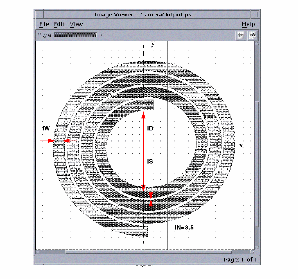
Two kinds of shapes of inductors are supported: squares and circles as shown in the following two figures.
Square Inductors
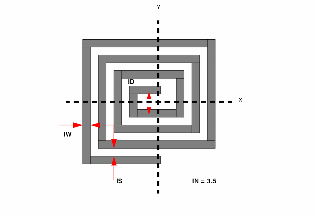
There are some constraints of the starting and ending points of the shapes.
- They should be either on the X or Y axis. In other words, the count of circles should be integral times of 1/4.
- Depending on the orientation of the circles, both ends of the shapes should be a little bit ahead of the axises to get a more accurate result of the extraction.
- The outside end of the loop of a square inductor should not extend past the outside edge of the inductor body.
Circular Inductors
Supporting More Geometric Parameter Extraction for Box Elements Using the PARSET and LEXTRACT Commands
By default, the Dracula product extracts the AREA and PERI parameters for box elements. In this version and subsequent versions, you can extract more geometric parameters for a box element. The allowable parameters are ANG, AREA, PERI, OVPR, OVAR, ID, IN, IW, and IS. To extract parameters other than AREA and PERI, you have to use the PARSET command to specify what parameters will be extracted, followed by the ELEMENT BOX command. You define the PARSET command in the “Operation Block Commands” section and you define the ELEMENT BOX command in the “Description Block Commands” section of your rules file. Then, you have to use the Dracula flexible LPE commands LEXTRACT and EQUATION to explicitly specify the parameters extracted for a box element.
Selective LPE
Selective LPE extracts layout parasitics and devices associated with a path. The LPE-QUERY command runs selective LPE. LPE-QUERY is designed to run in both batch and incremental run modes.
In addition to parameter extraction, LPE-QUERY can also output the geometries associated with a node. Dracula performs LPE layout extraction with a node-based scheme. One advantage of this node-based extraction scheme is its efficiency in handling multiple path extraction with overlapped nodes. You need to specify and extract overlapped nodes only once.
A path is defined as a series of nodes or nets. You must define the node set that corresponds to the path you want to analyze. You can specify the nodes using schematic or layout node names or numbers. If you specify schematic node names or numbers, Dracula maps the schematic node names to corresponding layout node numbers to perform extraction. In this case, you must run LVS to establish a cross-reference before you use LPE-QUERY.
Use the following commands to run selective LPE:
-
LPE-QUERY = ON/CORE/EXPAND
Include this command in the Description block to turn on selective LPE. -
SELECT-MODE
Include this command in the Description block to indicate whether the node name or number is based on the schematic or layout. -
NODE-SELECT or NODE-FILTER
Include one of these commands in the Operation block.
For details about these commands, refer to
Selective LPE Batch Example
The example in this section shows the rules file for a selective LPE run in batch mode.
*DESCRIPTION
.
LPE-QUERY = ON
SELECT-MODE = SCH
.
*END
.
*OPERATION
.
;define element devices
.
;define parasitic devices
.
LPECHK
.
;extract first node set
.
NODE-SELECT = NET1 NET2 NET3
;OR
;NODE-FILE = CLOCK
LPESELECT CAP[C] &
LPESELECT CAP[B] OUTPUT SPICE1
.
;extract second node set
.
NODE-SELECT = NET4 NET5 NET6 OUTPUT CRITICAL 63
LPESELECT CAP[A] &
LPESELECT CAP[D] OUTPUT SPICE2
*END
Selective LPE Incremental Example
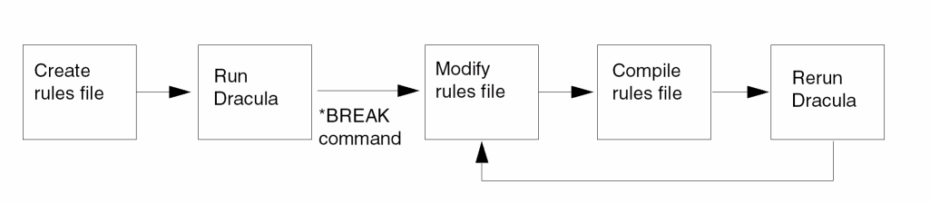
The example in this section shows the rules file for an incremental selective LPE run. If you need to analyze additional paths after finishing the current paths, incremental mode can reduce CPU time.
In incremental mode, the *BREAK command interrupts the run so you can modify the rules file to list a new node set, recompile the rules file, and rerun Dracula starting at the command after the *BREAK. Dracula does not repeat steps it has already performed, as shown in the following illustration.
*DESCRIPTION
.
LPE-QUERY = ON
SELECT-MODE = SCH
.
*END
.
*OPERATION
.
;define element devices
.
;define parasitic devices
.
LPECHK
.
;extract first node set
.
*BREAK INCRE            ;modify and recompile rules file
NODE-FILE = CLOCK       ;to extract next node set
LPESELECT CAP[C] &
LPESELECT CAP[B] OUTPUT SPICE1
.
;modify rules file to extract second node set
.
NODE-SELECT = NET4 NET5 NET6
LPESELECT CAP[A] &
LEPSELECT CAP[D] OUTPUT SPICE2
*END
LPE Examples
This section contains a rules file used to extract electrical parameters from an IC layout. LPE extracts the parasitic capacitance of a node, the area and perimeter of a diode, and the gate size of a MOS transistor. LPE creates a netlist that you can use to check the consistency of layout to circuit simulation, circuit and logic-level simulation, and timing verification. The sample problem uses many features of LPE but does not represent all possible combinations. Following this example are sample CMOS and NMOS rules files to use with LPE.
Features of the Example
The example is a circuit processed in silicon-gate CMOS technology. The key features of the problem are as follows:
- Ptwell and ntnsub pseudo contact layers are created by logicals to make connections between P-well and the P+ diffusion layer and between substrate and the N+ diffusion layer. (If there is no possible connection to the substrate or well, you can use a LINK command to force the substrate or well to connect to a text layout label, such as VCC or GND.)
-
The example specifies two kinds of transistors.
-
The example specifies two kinds of parasitic diodes.
P+ diffusion in nsub substrate with substrate-ties discarded
-
The example specifies seven kinds of parasitic capacitances.
The LPECHK command starts LVS consistency checking and backannotates the extracted SPICE list with the schematic names.
The LPESELECT command assigns values in the extracted SPICE list during the LPE run. You can also generate this SPICE list with LPEPRO.
Rules File in a MOS Example
This section describes the construction of an LPE rules file for a silicon-gate CMOS process technology. An LPE rules file is an extension of an ERC or LVS rules file. The file contains three blocks: the Description block, the Input-Layer block, and the Operation block. Samples of these blocks follow, with explanations of their major commands.
The Description Block
Description block commands are similar to DRC, ERC, and LVS commands. The major commands required for LPE include the following:
Specifies the parasitic diode parameters A1 and P1 (area and perimeter). The default is A1 and P1.
Specifies the MOS and diode SPICE model (type) in the SPICE listing. If you do not specify MODEL, all MOS and diode statements become comments in the SPICE listing.
Specifies the parasitic capacitor unit such as pf, picofarad. The default reports the natural unit on the layout.
Use in conjunction with the LPECHK command. Specify only if an LVS verification check command provides a schematic netlist. The default SPICE listing is based on text layout labels.
; ******************************************************
; SILICON GATE CMOS LPE RUN
; INPUT RULES FILE
; ******************************************************
*DESCRIPTION
OUTDISK = LPEOUT          ; Graphic error cell file name
PRIMARY = ECAD            ; Top cell name
MODE = EXEC NOW           ; Mode execution card
SYSTEM = GDS2             ; Graphic CAD database format
PROGRAM-DIR = QA:         ; Program directory of Cadence modules
SCALE = .001 MICRON       ; Graphic database scale
RESOLUTION = .25 MICRON   ; Database digitized grid unit
PRINTFILE = LPEPRT        ; Print file name of DRACULA run
;
DIODESEQ = A1 P1          ; Spice diode parameter sequence card
MODEL = MOS[N],N MOS[P],P DIO[N],N DIO[P],P  ; Spice transistor &
                          ; diode model specifications
UNIT = CAPACITANCE,PF     ; Spice capacitance unit
                          ; specification
;
SCHEMATIC = LVSLOGIC      ; Schematic netlist from LOGLVS
                          ; compiler
*END
Input-Layer Block
The major commands for the Input-Layer block include the following:
Generates a new bulk layer, which generates the nsub layer. The substrate and well make up a terminal of most parasitic capacitors and diodes defined in Dracula. You can use the layer generated by SUBSTRATE to create “reverse field masks” by using logical operations.
If you do not draw and include a substrate layer in the layout database, as in the example, you must specify the Input-Layer block SUBSTRATE command to create reverse field masks. Dracula assigns the dimension of this substrate layer, but you can assign it yourself if you specify the WINDOW or the WINDOW-CUT=EDGE command. For more information, refer to Chapter 12, “Input-Layer Block Commands.”
Specifies the conductor layers that carry node information, as in ERC or LVS. If you used the CONNECT command in the Operation Block, CONNECT-LAYER is required.
The CONNECT-LAYER command also assigns the text-attaching sequence, which you can redefine with the TEXTSEQUENCE command. For layout texting requirements, refer to the layout texting procedure for running ERC or LVS. For additional information, refer to Chapter 12, “Input-Layer Block Commands.”
*INPUT-LAYER
;
DIFF = 2            ; Thin oxide regions
PWELL = 1           ; P-well regions
POLY = 3            ; Poly silicon
CONT = 5            ; Metal contacts
METAL = 6           ; Metal
VAPOX = 7 TEXT 30   ; Pad opening & text layer 30
PPLUS = 8           ; Layer created for the substrate
SUBSTRATE = BULK 63
;
CONNECT-LAY = NSUB PWELL PSD NSD POLY METAL
; *** The conductor layers of the CMOS process ***
*END
Operation Block
The major commands in the Operation block example are the same as those for running an LVS job with SUBSTRATE type checking. The layers in the CONNECT operations must appear in the CONNECT-LAYER command in the Input-Layer block.
;***********************************************************
; OPERATION BLOCK
;
; CREATE THE DEVICE LAYERS AND CONDUCTOR LAYERS
; **********************************************************
*OPERATION
AND DIFF PPLUS PREGION     ; All active P+ regions
NOT DIFF PREGION NREGION   ; All active N+ regions
AND POLY NREGION NGATE     ; N-Channel devices
NOT NREGION NGATE NSD      ; N+ source/drain & substrate ties
AND POLY PREGION PGATE     ; P-Channel devices
NOT PREGION PGATE PSD      ; P+ source/drain & p-well ties
AND VAPOX METAL BPAD       ; Bonding pad device
NOT BULK PWELL NSUB        ; Created N-substrate layer
AND PSD PWELL PTWELL       ; Pseudo P+ tie for P-well
NOT NSD PWELL NTNSUB       ; Pseudo N+ tie for N-substrate
;
;***********************************************************
; CONNECT OPERATION FOR CMOS PROCESS
;***********************************************************
;
CONNECT METAL POLY BY CONT
CONNECT METAL NSD BY CONT
CONNECT METAL PSD BY CONT
CONNECT PSD PWELL BY PTWELL
CONNECT NSD NSUB BY NTNSUB
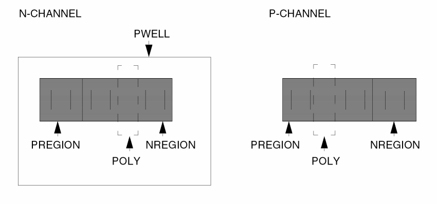
The following figure shows the layout of a MOS device in its original form (N-type and P-type).
The following figure shows the extracted layout after the program performs the logical operations to substrate. (1) is a pseudo P+ tie created by the program; (2) is a pseudo N+ tie created by the program.
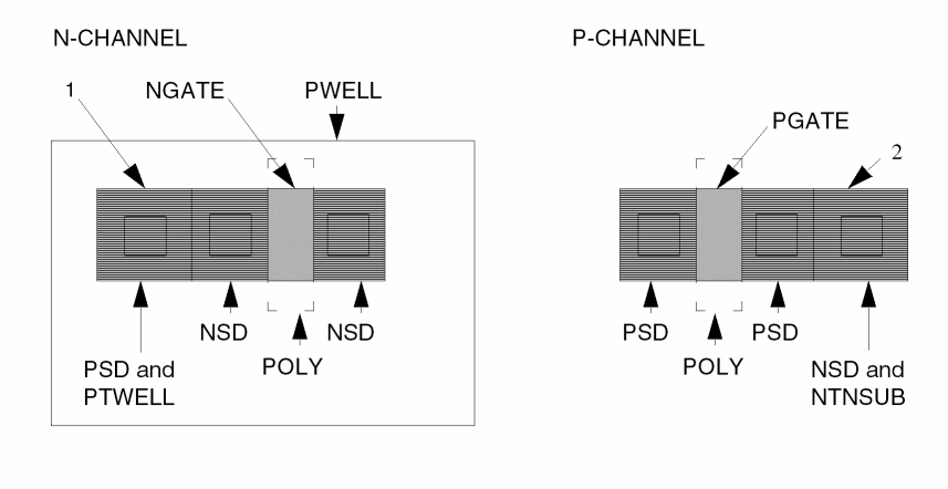
Connection of the pwell is made from node information from psd to pwell through ptwell, the generated contact layer. Connection of nsub is made from node information from nsd to nsub through ntnsub, the contact layer. Also, the nsub layer (substrate for the P-channel devices) is generated from the bulk layer specified by the SUBSTRATE command. This is also known as a “reverse mask operation.”
The major commands include the following:
Carry node information to the output generated layers because their field 1 layers carry node information. These generated layers are used for the device layers of the PARASITIC CAPACITOR and PARASITIC DIODE commands.
The PARASITIC DIO device layer includes only real diodes, not substrate or well ties. The device layer must not include any N+ or P+ ties or guard rings (in the previous figure, “1” and “2” denote a pwell tie and nsub tie, respectively). The logical operation that generated the ndio and pdio are N+ diode to the pwell and P+ diode to the nsub, respectively.
Specify the parasitic diodes and capacitors.
SPICE listing. For PARASITIC DIO, the PARASITIC CAP device layer must carry node information.
Assigns the capacitance value for each type of parasitic capacitor.
; OPERATION Block (Continued)
;
; ************************************************************
; LOGICAL OPERATION DEFINING THE PARASITIC CAPACITORS AND DIODES
; **************************************************************
;
AND METAL POLY MPOLY   ; Metal to poly capacitors
NOT METAL POLY METNP   ; Remove poly underneath metal
AND METNP NSD MNSD     ; Metal to N+ source/drain capacitors
AND METNP PSD MPSD     ; Metal to P+ source/drain capacitors
NOT METNP NSD M1
NOT M1 PSD M2          ; Further remove source/drain under metal
AND M2 PWELL MWELL     ; Metal to P-well capacitors
AND M2 NSUB MSUB       ; Metal to N-substrate capacitors
NOT POLY NGATE P1
NOT P1 PGATE P2        ; Remove channel region from poly
AND P2 PWELL POWELL    ; Poly to P-well capacitors
AND P2 NSUB POSUB      ; Poly to N-substrate capacitors
AND NSD PWELL NDIO     ; N+ diode to P-well minus the N+ ties
NOT PSD PWELL PDIO     ; P+ diode to N-substrate minus the P+ ties
;
; ************************************************************
; DEFINING TRANSISTOR ELEMENTS AND PARASITIC ELEMENTS
; ************************************************************
ELEMENT MOS[N] NGATE POLY NSD PWELL ;N-channel
ELEMENT MOS[P] PGATE POLY PSD NSUB  ;P-channel
ELEMENT PAD BPAD METAL              ;Pad element
PARASITIC DIO[N] NDIO PWELL NDIO    ;N+ diode to P-well
PARASITIC DIO[P] PDIO PDIO NSUB     ;P+ diode to N-substrate
PARASITIC CAP[A] MPOLY METAL POLY   ;Metal to poly capacitor &
ATTRIBUTE CAP[A] 0.00005            ;attribute (pf/sq micron)
PARASITIC CAP[B] MNSD METAL NSD     ;Metal to N+ capacitor &
ATTRIBUTE CAP[B] 0.00005            ;attribute (pf/sq micron)
PARASITIC CAP[C] MPSD METAL PSD     ;Metal to P+ capacitor &
ATTRIBUTE CAP[C] 0.00005            ;attribute (pf/sq micron)
PARASITIC CAP[D] MWELL METAL PWELL   ;Metal to P-well capacitor &
ATTRIBUTE CAP[D] 0.00005            ;attribute (pf/sq micron)
PARASITIC CAP[E] MSUB METAL NSUB    ;Metal to N-substrate
                                    ;capacitor &
ATTRIBUTE CAP[E] 0.00005            ;attribute (pf/sq micron)
PARASITIC CAP[F] POWELL POLY PWELL  ;Poly to P-well capacitor &
ATTRIBUTE CAP[F] 0.00005            ;attribute (pf/sq micron)
PARASITIC CAP[G] POSUB POLY NSUB    ;Poly to N-substrate
                                    ;capacitor &
ATTRIBUTE CAP[G] 0.00005            ;attribute (pf/sq micron)
The major commands include the following:
Starts LVS. Use LPECHK to backannotate an extracted SPICE listing with schematic names. If no schematic netlist exists, do not specify LPECHK; the extracted CDL listing is based on layout text and system-assigned internal node numbers.
Specifies the nospi SPICE list file. The example using the ampersand (&) shows separation of the device in the CDL listing. The [S] option backannotates the CDL listing with schematic names. This option has no meaning without the LPECHK command.
;OPERATION Block (Continued)
;
LPECHK                      ;Layout versus schematic
;
LPESELECT[S] MOS[P] &       ;SPICE output file for transistors
LPESELECT[S] MOS[N] &
LPESELECT[S] DIO[P] &
LPESELECT[S] DIO[N] &
LPESELECT[S] CAP[A] GT 0.0 &
LPESELECT[S] CAP[B] GT 0.0 &
LPESELECT[S] CAP[C] GT 0.0 &
LPESELECT[S] CAP[D] GT 0.0 &
LPESELECT[S] CAP[E] GT 0.0 &
LPESELECT[S] CAP[F] GT 0.0 &
LPESELECT[S] CAP[G] GT 0.0 OUTPUT NOSPI
;
*END
NMOS LPE Input File
;**********************************************************
;                 SILICON GATE NMOS LPE RUN
;                     INPUT RULES FILE
;**********************************************************
*DESCRIPTION
INDISK = inchip          ; Graphic database file
OUTDISK = lpeout         ; Graphic error database file
PRIMARY = top            ; Top cell name
MODE = exec now          ; Mode execution
SYSTEM = gds2            ; Graphic CAD database format
PROGRAM-DIR = usr1/dracula/bin/
                         ; Program directory of Dracula modules
SCALE = .001 micron      ; Graphic database scale factor
RESOLUTION = .5 micron   ; Graphic digitized grid increments
PRINTFILE = lpeprt       ; Print file name LPE run
;
DIODESEQ = a1 p1         ; Spice diode parameter sequence
MODEL= MOS[E],enh MOS[D],dep DIO[N],ndio   ; Spice transistor &
                         ; diode model specifications
UNIT= CAPACITANCE,pf     ; Spice capacitor unit specifier
SCHEMATIC = LVSLOGIC     ; Schematic netlist from LOGLVS
;
*END
;**********************************************************
;                   INPUT-LAYER BLOCK
;**********************************************************
*INPUT-LAYER
diff = 1           ; Thin oxide region
depl = 2           ; Depletion VT adjust implant
bcc = 3            ; Buried contact for poly to diffusion
poly =4            ; Polysilicon
mcc = 5            ; Metal contacts
metal =6 TEXT 30   ; Metal & Text layer 30
pad = 7            ; Pad opening
;
CONNECT-LAYER= srcdrn poly metal
;*** The conductor layers of the NMOS process ***
;
SUBSTRATE psub 63  ; Create p - substrate layer
*END
;**********************************************************
;                      OPERATION BLOCK
;        CREATE THE DEVICE LAYERS AND CONDUCTOR LAYERS
;**********************************************************
*OPERATION
AND diff poly gbc
NOT gbc bcc gate        ; All transistors
NOT diff gate srcdrn    ; N + source/drain layer
AND gate depl dgate     ; Depletion devices
NOT gate dgate egate    ; Enhancement devices
AND pad metal padwin    ; Bonding pad
;**********************************************************
         CONNECT OPERATION FOR NMOS PROCESS
;**********************************************************
CONNECT metal poly BY mcc
CONNECT metal srcdrn BY mcc
CONNECT srcdrn poly BY bcc
LINK psub TO vss        ; Link the p - substrate to VSS
;**********************************************************
       LOGICAL OPERATION TO DEFINE THE PARASITIC
;                   CAPACITORS AND DIODE
;**********************************************************
AND metal poly mpoly    ; Metal to poly capacitor
NOT metal poly metnp    ; Remove poly from metal
AND metnp srcdrn msd    ; Metal to source/drain capacitors
NOT metnp srcdrn metsub ; Remove source/drain from metal
;
NOT poly gate polysub   ; Poly to substrate capacitors
;**********************************************************
;                DEFINING TRANSISTOR ELEMENTS
;           AND PARASITIC ELEMENT OF NMOS PROCESS
;**********************************************************
ELEMENT MOS[D] dgate poly srcdrn psub ; Depletion device
ELEMENT MOS[E] egate poly srcdrn psub ; Enhancement device
;
ELEMENT PAD padwin metal  ; Pad element
;
PARASITIC DIO[N] srcdrn psub srcdrn ; N + diode to p-substrate
PARASITIC CAP[A] mpoly metal poly   ; Metal to poly capacitor &
ATTRIBUTE CAP[A] 0.0005             ; attribute( pF/micron )
PARASITIC CAP[B] msd metal srcdrn   ; Metal to source/drain
ATTRIBUTE CAP[B] 0.0005             ; capacitor & attribute
;                                   ; ( pF/sq micron )
PARASITIC CAP[C] metsub metal psub  ; Metal to p-substrate
ATTRIBUTE CAP[C] 0.0002             ; capacitor & attribute
;                                   ; ( pF/sq micron )
PARASITIC CAP[D] polysub poly psub  ; Poly to p-substrate
ATTRIBUTE CAP[D] 0.0005             ; capacitor & attribute
;                                   ; ( pF/sq micron )
LPECHK             ; Layout versus schematic check
LPESELECT[S] MOS & ; SPICE-like netlist of
;                  ; transistors, diodes, and
LPESELECT[S] DIO & ; capacitors in file name,
LPESELECT[S] CAP GT 0.0 OUTPUT simon ; SIMON.DAT
*END
CMOS LPE Input File
;*********************************************************
;             SILICON GATE CMOS LPE RUN
;                 INPUT RULES FILE
;*********************************************************
*DESCRIPTION
INDISK = inchip          ; Graphic database file name
OUTDISK = lpeout         ; Graphic error cell file name
PRIMARY = top            ; Top cell name
MODE = exec now          ; Mode execution
SYSTEM = gds2            ; Graphic CAD database format
PROGRAM-DIR = usr1/dracula/bin/
                         ; Program directory of Dracula modules
SCALE = .001 micron      ; Graphic database scale
RESOLUTION = .5 micron   ; Database digitized grid unit
PRINTFILE = lpeprt       ; Print file name of DRACULA run
;
DIODESEQ = a1 p1         ; diode parameter sequence
MODEL = MOS[N],n MOS[P],p DIO[N],n DIO[P],p
;                        ; transistor & diode model
;                        ; specifications
UNIT = capacitance,pf    ; capacitance unit specification
SCHEMATIC = LVSLOGIC     ; Schematic netlist from LOGLVS compiler
*END
;*********************************************************
;   INPUT-LAYER BLOCK
;*********************************************************
*INPUT-LAYERS
diff = 1            ; Thin oxide regions
pwell = 2           ; P-well regions
poly = 3            ; Polysilicon
nplus = 4           ; N + implant
pplus = 5           ; P + implant
cont = 6            ; Metal contacts
metal = 7           ; Metal
vapox = 8 TEXT=28   ; Pad opening & Text layer 28
SUBSTRATE = bulk 63 ; Layer created for reverse mask
CONNECT-LAYER = nsub pwell psd nsd poly metal
;*** The conductor layers of the CMOS Process. ***
*END
;***************************************************************
;                    OPERATION BLOCK
;       CREATE THE DEVICE LAYERS AND CONDUCTOR LAYERS
;***************************************************************
*OPERATION
AND diff nplus nregion           ; All active N + regions
AND poly nregion ngate           ; N-Channel devices
NOT nregion ngate nsd            ; N+ source/drain & taps
;
AND diff pplus pregion           ; All active p + regions
AND poly pregion pgate           ; P-Channel devices
NOT pregion pgate psd            ; P+ source/drain & taps
;
AND vapox metal bpad             ; Bonding pad device
;
NOT bulk pwell nsub              ; Created N-Substrate layer
;
AND psd pwell ptwell             ; Pseudo P+ tap for P-well
;
SELECT nsd OUTSIDE pwell ntnsub  ; Pseudo N+ tap for N-Substrate
;
;*********************************************************
;               CONNECT OPERATION FOR CMOS PROCESS
;*********************************************************
CONNECT metal poly BY cont
CONNECT metal nsd BY cont
CONNECT metal psd BY cont
CONNECT psd pwell BY ptwell
CONNECT nsd nsub BY ntnsub
;*********************************************************
;          LOGICAL OPERATION DEFINING THE
;          PARASITIC CAPACITORS AND DIODES
;*********************************************************
AND metal poly mpoly   ; Metal to poly capacitors
NOT metal poly metnp   ; Remove poly underneath metal
AND metnp nsd mnsd     ; Metal to N+source/drain capacitors
AND metnp psd mpsd     ; Metal to P+source/drain capacitors
NOT metnp nsd m1
NOT m1 psd m2          ; Further remove source/drain under metal
AND m2 pwell mwell     ; Metal to p-well capacitors
AND m2 nsub msub       ; Metal to n-substrate capacitors
NOT poly ngate p1
NOT p1 pgate p2        ; Remove channel region from poly
AND p2 pwell powell    ; Poly to p-well capacitors
AND p2 nsub posub      ; Poly to n-substrate capacitors
AND nsd pwell ndio     ; N+diode to p-well minus taps
NOT psd pwell pdio     ; P+diode to n-substrate minus taps
;*********************************************************
;         DEFINING TRANSISTOR ELEMENTS AND
;                 PARASITIC ELEMENTS
;*********************************************************
ELEMENT MOS[N] ngate poly nsd pwell  ; N-Channel device
ELEMENT MOS[P] pgate poly psd nsub   ; P-Channel device
ELEMENT PAD bpad metal               ; Pad element
;
;
PARASITIC DIO[N] ndio pwell ndio     ; N+diode to p-well
PARASITIC DIO[P] pdio pdio nsub      ; P+diode to n-substrate
;
PARASITIC CAP[A] mpoly metal poly    ; Metal to poly capacitor &
ATTRIBUTE CAP[A] 0.00005             ; attribute( pF/micron )
PARASITIC CAP[B] mnsd metal nsd      ; Metal to n+capacitor &
ATTRIBUTE CAP[B] 0.00005             ; attribute( pF/sq micron )
PARASITIC CAP[C] mpsd metal psd      ; Metal to p+capacitor &
ATTRIBUTE CAP[C] 0.00005             ; attribute( pF/sq micron )
PARASITIC CAP[D] mwell metal pwell   ; Metal to p-well capacitor &
ATTRIBUTE CAP[D] 0.00005             ; attribute( pF/sq micron )
PARASITIC CAP[E] msub metal nsub     ; Metal to n-substrate
ATTRIBUTE CAP[E] 0.00005             ; capacitor & attribute
;                                    ; ( pF/sq micron )
PARASITIC CAP[F] powell poly pwell   ; Poly to p-well capacitor &
ATTRIBUTE CAP[F] 0.00005             ; attribute( pF/sq micron )
PARASITIC CAP[G] posub poly nsub     ; Poly to n-substrate
ATTRIBUTE CAP[G] 0.00005             ; capacitor & attribute
;                                    ; ( pF/sq micron )
LPECHK                               ; Layout versus schematic
;                                    ; check
;
LPESELECT[S] MOS &                   ; SPICE output file for
;                                    ; transistors, diodes,
LPESELECT[S] DIO &                   ; and capacitors in an
LPESELECT[S] CAP GT 0.0 OUTPUT spice ; output file, SPICE.DAT
*END
Hierarchical LPE
Hierarchical Layout Parameter Extraction (HLPE) extracts circuit elements and parasitic devices using Hcells. The commands for circuit extractions are the same as those in the LPE flat mode. You can run HLPE in cell and composite modes with the same commands and concepts as in HLVS.
HLPE extracts and reports circuit device sizes and parasitic information from the layout. It outputs in SPICE/CDL format a subcircuit listing for each Hcell with its own parasitics and a top subcircuit listing with calls (instantiations) to the hierarchical cells. The output is a description of the circuit in a two-level hierarchy. You can do backannotation to schematic netlist if you input a schematic netlist and run HLVS together with HLPE (just as when LVS is run jointly with LPE in a flat mode run).
To generate a subcircuit listing of Hcells, run cell mode HLPE with all cell pin text. You can then run composite mode HLPE to generate the top-level netlist with subcircuit calls.
To compare the ratio of device area to the layer area driving the devices, you can do an antenna check. This check helps ensure that induced capacitance, caused by a fabrication process or a circuit operation, does not cause the drive current or the transition time to become unstable.
To run an antenna check with HLPE
When running composite mode, COMPUTE reads the parameter file generated by the cell mode and adds the data to the composite plane for each cell instance.
See the LEXTRACT, COMPUTE, and CHKPAR commands for more information about antenna checks.
Cell Mode
Cell mode generates the SPICE.CEL file containing subcircuit listings of the hierarchical cells specified in cell.tab and schematic names with parasitics and MOS device sizes.
If you want back-annotation to schematics, input a schematic netlist with an Hcell table to LOGLVS and run the same as a flat mode run.
Composite Mode
Composite mode HLPE generates a SPICE.DAT file containing top level devices with parasitics and subcircuit calls to the hierarchical cells. If you run the job in the same directory that you used for the cell mode run and the SPICE.CEL file exists, Dracula creates SPICE.DAT by appending the composite mode output to SPICE.CEL so that it becomes a complete netlist of the layout circuit.
Return to top