2
Sample Parameterized Cells Reference
This chapter discusses the following:
- Modifying Pcell Parameter Values
- spcbentnmos, spcbentpmos
- spccap
- spcinv
- spcnmos, spcpmos
- spcnpn
- spcpnp
- spcpres
- spcres
- spcsimple_nmos, spcsimple_pmos
Modifying Pcell Parameter Values
Once you have installed the sample Pcells, you can place instances of them in your layout and modify their parameters to suit your specifications. When you place an instance using the Create Instance form (choose Create – Instance), the system prompts you to enter values for a variety of parameters or to accept the defaults. You can modify an instance using the Edit Properties form (choose Edit – Properties) as well.
Each section in this chapter consists of a brief discussion of a sample Pcell and a description of its parameters as they appear in the Create Instance and Edit Properties forms. Each parameter entry contains information about the purpose and default value of the parameter. When appropriate, some entries also provide information about valid parameter values and examples of such values.
Default Values
During the installation, you assigned values to design rules and then saved them to the techParams subclass of the controls class of the technology file. The default values for many of the parameters of the sample Pcells are derived from these same values.
For instance, the gate length of the spcbentnmos device defaults to the minimum width of the poly layer (minWidth poly), which you specified during the installation. The values that you can specify for many of the parameters are bounded by these same technology file values.
spcbentnmos, spcbentpmos
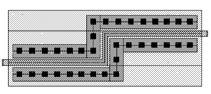
The spcbentnmos device is an NMOS transistor with a bent-gate option, and the spcbentpmos device is the PMOS equivalent. The parameter Coordinate list allows you to modify the path of the gate by specifying the coordinates of the center of the gate.
This section discusses the spcbentnmos/spcbentpmos device parameters that appear in the Create Instance (choose Create – Instance) and Edit Properties (choose Edit – Properties) forms of the Virtuoso® layout editor. The
Parameters
|
Controls the width of the gate. When Coordinate list has values specified, Gate Width is derived from those values.
Valid Values: a number in meters, in engineering notation, greater than or equal to the value of |
|
|
Controls the length of the gate. |
|
|
The Virtuoso layout accelerator (Virtuoso XL) supports the use of the |
|
|
Defines the X and Y coordinates of the gate path. |
|
|
Adds source contacts. The Source Contact Position and Source Contact Coverage parameters appear when Source Contacts? is on. |
|
|
Adds drain contacts. The Drain Contact Position and Drain Contact Coverage parameters appear when Drain Contacts? is on. |
|
|
Positions the contacts vertically within the source. When the contacts are not spread out evenly along the width of the source, you can shift the contacts toward the top, center, or bottom of the source, relative to the unrotated device. |
|
|
Positions the contacts vertically within the drain. When the contacts are not spread out evenly along the width of the drain, you can shift the contacts toward the top, center, or bottom of the drain, relative to the unrotated device. |
|
|
Controls the percentage of the width of the source that the contacts cover. This lets you route other metal lines across the device without connecting them to it electrically. |
|
|
Controls the percentage of the width of the drain that the contacts cover. This lets you route other metal lines across the device without connecting them to it electrically. |
|
|
Connects the bulk-substrate to source or drain. |
|
spccap
The spccap device is an array capacitor. You can change the aspect ratio of the array by adjusting the number of rows and columns. You can round up the unit capacitance value or add an extra capacitor to the array to achieve the precise required capacitance value.
This section discusses the spccap device parameters that appear in the Create Instance (choose
Parameters
|
Controls the required capacitance.
Valid Values: a number in farads, in engineering notation, greater than or equal to the value of |
|
|
Specifies the total capacitance of all the unit capacitors in the Pcell. This is a noneditable field. |
|
|
Builds the Pcell of multiple-unit capacitor tiles. |
|
|
Controls the internal layout of multiple-unit capacitors within the Pcell. |
|
|
Controls the number of rows of unit capacitors within the Pcell. |
|
|
Controls the number of columns of unit capacitors within the Pcell. |
|
|
Controls the required capacitance for the unit capacitors within the Pcell. |
|
|
Rounds the capacitance value to the next higher unit of capacitance. Cap Round Up? and Add Extra cannot both be on at the same time. |
|
|
Adds an extra capacitor to achieve the required capacitance. Add Extra and Cap Round Up? cannot both be on at the same time. |
|
|
Virtuoso XL supports the use of the |
|
spcinv
The spcinv device is an inverter built using the spcnmos and the spcpmos devices. You can modify the gate width and length of both transistors, define the supply width, and set the height of the whole cell. Note the stretch handles that let you graphically scale the device.
This section discusses the spcinv device parameters that appear in the Create Instance (choose Create – Instance) and Edit Properties (choose Edit – Properties) forms of the Virtuoso layout editor. The
Parameters
spcnmos, spcpmos
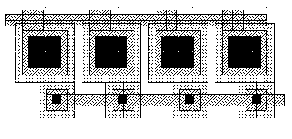
The spcnmos device is an n-diffusion straight-gate MOS transistor, and the spcpmos device is the p-diffusion equivalent. You can modify the gate width and length of the transistor, apply fingered or threshold gate splitting, add contacts to either side of the gate, and specify the position of the source and drain contacts.
This section discusses the spcnmos/spcpmos device parameters that appear in the Create Instance (choose Create – Instance) and Edit Properties (choose Edit – Properties) forms of the Virtuoso layout editor. The
Parameters
|
Controls the width of the gate. |
|
|
Controls the length of the gate. |
|
|
Virtuoso XL supports the use of the |
|
|
Splits the gate. The Type of Splitting, Number of Fingers (or Threshold Value if Type of Splitting is set to Threshold), and Internally connect poly? parameters appear when Gate Splitting is on. |
|
|
Controls how the gate is split. |
|
|
Controls the number of fingers in the transistor. |
|
|
Specifies the maximum width for each gate when Gate Splitting is on. |
|
|
Adds contacts to the left of each gate relative to the unrotated device. The left contact is always the source contact. If you set Number of Fingers to an even number, the source contacts and drain contacts alternate, starting with a source contact to the left of the left-most gate (relative to the unrotated device). |
|
|
Adds contacts to the right of each gate relative to the unrotated device. If you set Number of Fingers to an odd number, the right contact is a drain. If you set Number of Fingers to an even number, the source contacts and drain contacts alternate, starting with a source contact to the left of the left-most gate (relative to the unrotated device). |
|
|
Adds substrate contacts. The Substrate Contact Position parameter appears when Add substrate contact? is on. If Bulk Node Connection is set to S, the substrate contact is positioned to the left of the gate, relative to the unrotated device. If Bulk Node Connection is set to D, the substrate contact is positioned to the right of the gate, relative to the unrotated device. |
|
|
Positions the substrate contact relative to the unrotated device. |
|
|
Connects the bulk substrate to the source or drain. |
|
|
Connects the poly gates to each other within the Pcell. |
|
|
Positions the poly gate connection relative to the unrotated device. |
|
|
Connects the source or the drain to metal. |
|
spcnpn
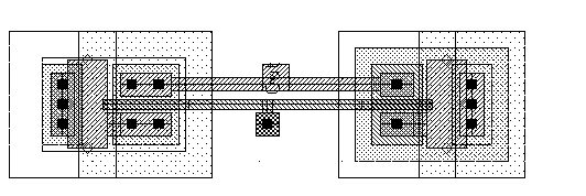
The spcnpn device is an NPN bipolar transistor that, given the wide variety of bipolar transistor designs, has been kept fairly simple. There are five choices of collector, emitter, and base configurations and a parameter for the emitter width. Note the stretch handles that let you graphically scale the device.
This section discusses the spcnpn device parameters that appear in the Create Instance (choose Create – Instance) and Edit Properties (choose Edit – Properties) forms of the Virtuoso layout editor. The
Parameters
|
Chooses the collector-base-emitter configuration. |
|
|
Controls the width of the emitter. |
|
|
Virtuoso XL supports the use of the |
spcpnp
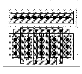
The spcpnp device is a stretchable PNP bipolar transistor that, given the wide variety of bipolar transistor designs, has been kept fairly simple. The Pcell contains the emitter and the base. The collector is a zero-level multipart path built with the ROD function rodCreatePath.
This section discusses the spcpnp device parameters that appear in the Create Instance (choose Create – Instance) and Edit Properties (choose Edit – Properties) forms of the Virtuoso layout editor. The
Parameters
|
Controls the width of the gate.
Valid Values: a number in meters, in engineering notation |
|
|
Controls the number of emitters in the Pcell. |
|
|
Selects the access direction of the emitter. |
|
|
Virtuoso XL supports the use of the |
|
spcpres
Sometimes resistors in a schematic represent estimates of the resistance that certain signals might have after the layout designer draws the design. Including these resistors helps improve the simulation results. During layout, the designer does not draw the resistor because it represents the resistance of the shapes needed to connect the other components.
Virtuoso XL expects the layout to match the schematic device for device and net for net. The spcpres device was designed to let you place a resistor in the schematic and connect separate nets to each side of the device, without causing Virtuoso XL to expect to see a corresponding resistor in the layout.
The spcpres device uses the sheet resistance (sheetRes) from the technology file for the metal layer and adjusts the device size accordingly. Given the low resistance of the metal layer, you need to enter relatively large values to see a visible change in the layout view. The pins are never placed more than twice the minimum grid spacing apart. The separation between the pins prevents the Virtuoso XL connectivity extractor from reporting a short where the two nets touch. Note the stretch handles that let you graphically scale the device.
Parameters
|
Specifies the input that defines the resistor. |
|
|
Controls the total resistance of the device. |
|
|
Controls the length of the resistor path. |
|
|
Controls the width of the resistor path. |
|
|
Virtuoso XL supports the use of the |
spcres
The spcres device is a resistor built to let you define the type of resistor material (poly, n-diffusion, or p-diffusion), resistance, length, and width. You can draw the resistor in a serpentine or strap formation for layout optimization.
This section discusses the spcres device parameters that appear in the Create Instance (choose Create – Instance) and Edit Properties (choose Edit – Properties) forms of the Virtuoso layout editor. The
Parameters
|
Controls the total resistance of the device. |
|
|
Controls the length of the resistor path. |
|
|
Specifies the input that defines the resistor. |
|
|
Controls the width of the resistor path. |
|
|
Selects the shape of the resistor. Choose Straps to draw the resistor with the number of resistor paths specified in Number of segments between the contacts. Choose Serpentine to draw the resistor path in an accordion shape with the specified number of segments. |
|
|
Controls the number of straps or serpentine segments. When you set Draw resistor as to Straps, Number of segments controls how many resistor paths the system draws between the serially connected contacts. When you set Draw resistor as to Serpentine, Number of segments controls how many segments are in the accordion shape of the resistor path. |
|
|
Controls the width of the serpentine resistor path. |
|
|
Virtuoso XL supports the use of the |
spcsimple_nmos, spcsimple_pmos
The spcsimple_nmos and spcsimple_pmos devices are simpler implementations of transistors than the spcnmos and spcpmos devices.
These simpler devices do not support wells and substrate contacts, and the contact choices are more limited. The contact coverage and the choice to have contacts are merged into a single contact coverage parameter, which is set in a cyclic field.
The splitting variable in the spcnmos and spcpmos devices that later prompts you for the number of fingers was replaced with a single parameter in the spcsimple_nmos and spcsimple_pmos devices. Any value larger than 1 in the Number of Fingers field splits the device. There is no choice of types of splitting. Note the stretch handles that let you graphically scale the device.
These devices support relative object design (ROD) commands, Virtuoso XL permutable pins and device abutment, and pin connection modeling (strong, weak, and must-join) for the Virtuoso custom router. These devices are not compatible with the Virtuoso compactor or the Virtuoso layout synthesizer.
Parameters
|
Controls the width of the gate.
Valid Values: a number in meters, in engineering notation, greater than or equal to the value of |
|
|
Controls the length of the gate. |
|
|
Virtuoso XL supports the use of the |
|
|
Controls the number of fingers in the transistor. |
|
|
Specifies the maximum width for each gate when Number of Fingers is greater than 1. |
|
|
Positions the contacts vertically. When the contacts are not spread out evenly along the width of the drain, you can shift the contacts toward the top, center, or bottom of the drain, relative to the unrotated device. |
|
|
Controls the percentage of the width of the left side of the device that the contacts cover. This lets you route other metal lines across the device without connecting them to it electrically. |
|
|
Positions the contacts vertically. When the contacts are not spread out evenly along the width of the drain, you can shift the contacts toward the top, center, or bottom of the drain, relative to the unrotated device. |
|
|
Controls the percentage of the width of the device that the right side contacts cover. This lets you route other metal lines across the device without connecting them to it electrically. |
|
|
Positions the center contact, if there is more than one finger. |
|
|
Controls the right side contacts coverage, if there is more than one finger. This lets you route other metal lines across the device without connecting them to it electrically. |
|
Return to top