11
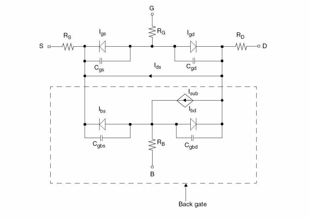
JFET Model (jfet)
The JFET model is derived from the FET model of Shichman and Hodges. This topic contains the following information for the JFET model:
where
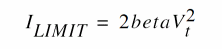
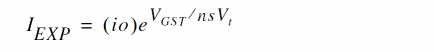
Drain Current for the Subthreshold Region
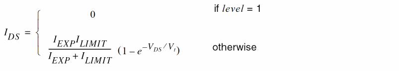
where
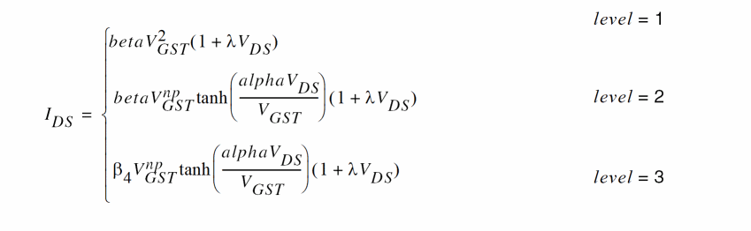
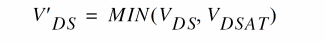
Drain Current for the Triode Region
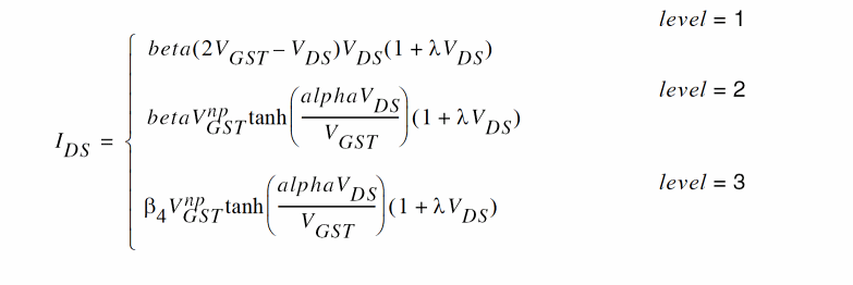
where
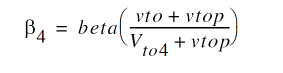
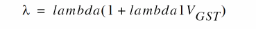
Drain Current for the Saturation Region
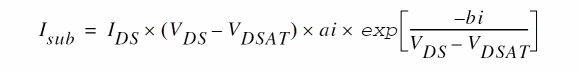
Substrate Leakage Currents
If ai and bi are both greater than 0, and VDS>VDSAT,
For information on bulk junction models IBS, IBD, CGBS, and CGBD, see Common MOSFET Equations
Gate Junction Currents
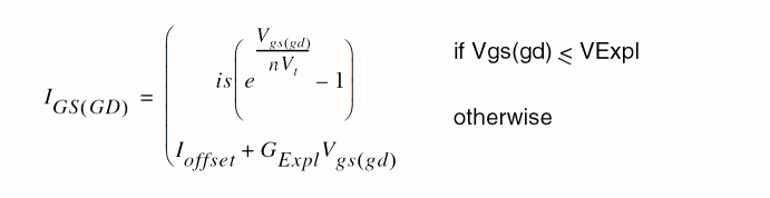
where Vt is the thermal voltage given by
 ,
,
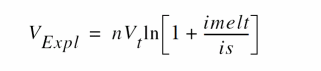
is the forward explosion voltage,
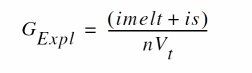
is the conductance at VExpl, and
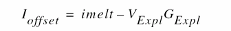
is the current linearly extrapolated to V = 0 from VExpl.
Gate Junction Capacitance
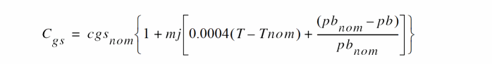
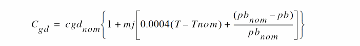
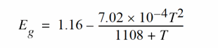
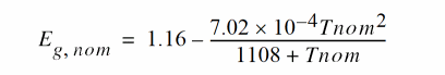
Temperature Effect
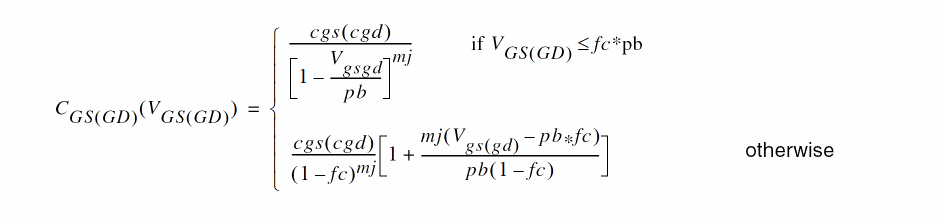
Gate-Source and Gate-Drain Capacitance
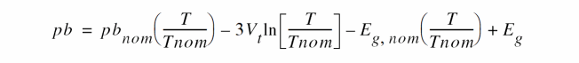
Junction Potential
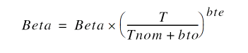
Transconductance Temperature
Gate Junction Current
where, if SPICE-compatibility is required (set by the options),
otherwise,
For equations on parameters tlev, tlevc, gap1, and gap2, see Common MOSFET Equations
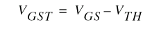
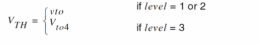
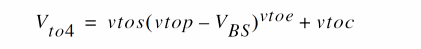
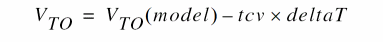
Threshold Voltage
For tcv,

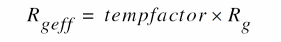
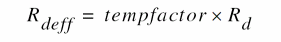
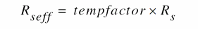
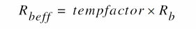
Parasitic Resistors

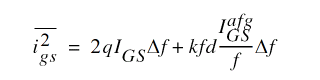
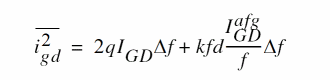
Noise Model
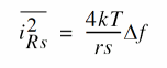
Source Series Resistance Thermal Noise
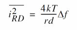
Drain Series Resistance Thermal Noise
Channel Thermal and Flicker Noise
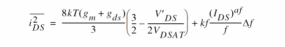
where
gm is the transconductance, gds is the channel conductance, kf and af are constants for a given device. The Spectre® circuit simulator defaults for kf and af are 0.0 and 1.0, respectively.
Gate Junction Noise
Scaling Effects
The following are the Spectre scaling effects:
-
is, cgs, cgd, and beta are multiplied by area.
-
rs and rd are divided by area.
-
All noises are multiplied by area.
Component Statements
Sample Instance Statement:
jf1 (net1 net2 0) jmod area=1
Sample Model Statement
model jmod jfet beta=9e-5 lambda=0 type=n vt0=-18.7 rd=10 rs=10 cgs=1.3e-13 pb=0.65
Instance Syntax
Name d g s [b] ModelName parameter=value ...
You do not have to specify the back gate terminal when you use the four-terminal model. If left unspecified, the substrate is connected to ground.
Instance Parameters
|
area=1
|
Junction area factor.
|
|
m=1
|
Multiplicity factor.
|
|
region=triode
|
Estimated operating region. Spectre generates output number (0-4) in a rawfile. Possible values are off, triode, sat, subth, or breakdown.
|
|
isnoisy=yes
|
Should resistor generate noise. Possible values are no or yes.
|
|
trise=0
|
Temperature rise from ambient.
|
|
dtemp=0
|
Alias of trise.
|
Model Syntax
model modelName jfet parameter=value ...
Model Parameters
Device type parameters
|
type=n
|
Transistor type. Possible values are n or p.
|
Drain current model parameters
|
level=1
|
Drain current model level selector.
|
|
vto=-2 V
|
Pinchoff voltage.
|
|
beta=0.0001 A/V2
|
Transconductance parameter.
|
|
lambda=0 1/V
|
Channel length modulation parameter.
|
|
lambda1=0 1/V
|
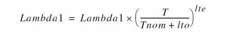
Gate dependence of channel length modulation parameter.
|
|
np=2
|
Power-law exponent.
|
|
alpha=2
|
Triode-to-saturation transition parameter.
|
|
io=0 A
|
Subthreshold current parameter.
|
|
ns=1
|
Subthreshold swing parameter.
|
|
ai=0 1/V
|
Impact ionization current coefficient.
|
|
bi=0 V
|
Impact ionization current exponent.
|
Four terminal threshold voltage parameters
|
vtop=0.6 V
|
Back gate to channel junction potential.
|
|
vtos=1.2 V
|
Threshold voltage slope.
|
|
vtoe=0.33
|
Threshold voltage exponent.
|
|
vtoc=-3.3 V
|
Threshold voltage constant.
|
Parasitic resistance parameters
|
rd=0 Ω
|
Drain resistance (/area).
|
|
rs=0 Ω
|
Source resistance (/area).
|
|
rg=0 Ω
|
Gate resistance (/area).
|
|
rb=0 Ω
|
Back gate resistance (/area).
|
|
minr=0.1 Ω
|
Minimum source/drain/gate resistance.
|
Junction diode model parameters
|
is=1e-14 A
|
Gate saturation current (*area).
|
|
n=1
|
Emission coefficient for G-D and G-S junctions.
|
|
imelt=`imax' A
|
Explosion current (*area).
|
|
dskip=yes
|
Use simple piece-wise linear model for diode currents below 0.1*iabstol. Possible values are no or yes.
|
Junction capacitance model parameters
|
tt=0 s
|
Transit time.
|
|
cgs=0 F
|
Gate-source zero-bias junction capacitance (*area).
|
|
cgd=0 F
|
Gate-drain zero-bias junction capacitance (*area).
|
|
mj=1/2
|
Junction grading coefficient.
|
|
pb=1 V
|
Gate-junction potential.
|
|
fc=0.5
|
Junction capacitor forward-bias threshold.
|
Four terminal junction parameters
|
isb=1e-14 A
|
Back gate-saturation current (*area).
|
|
nb=1
|
Emission coefficient for back gate-junctions.
|
|
cgbs=0 F
|
Back gate-source zero-bias junction capacitance (*area).
|
|
cgbd=0 F
|
Back gate-drain zero-bias junction capacitance (*area).
|
|
mjb=1/2
|
Back gate-junction grading coefficient.
|
|
pbb=1 V
|
Back gate-junction potential.
|
Temperature effect parameters
|
tnom (C)
|
Parameters measurement temperature. Default set by options.
|
|
trise=0 C
|
Temperature rise from ambient.
|
|
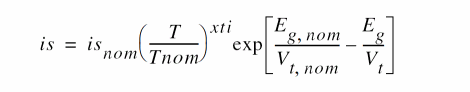
xti=3
|
Temperature exponent for effect on is.
|
|
tlev=0
|
DC temperature selector.
|
|
tlevc=0
|
AC temperature selector.
|
|
eg=1.12452 V
|
Energy band gap.
|
|
gap1=7.02e-4 V/C
|
Band gap temperature coefficient.
|
|
gap2=1108 C
|
Band gap temperature offset.
|
|
eglev=0
|
DC temperature selector.
|
|
tcv=0 1/C
|
Threshold voltage temperature coefficient.
|
|
bto=0 C
|
Transconductance parameter temperature offset.
|
|
bte=0
|
Transconductance parameter temperature exponent.
|
|
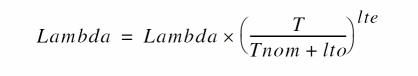
lto=0 C
|
Channel length modulation parameters temperature offset.
|
|
lte=0
|
Channel length modulation parameters temperature exponent.
|
|
tc1=0 1/C
|
Linear temperature coefficient for parasitic resistors.
|
|
tc2=0 C-2
|
Quadratic temperature coefficient for parasitic resistors.
|
|
pta=0 V/C
|
Junction potential temperature coefficient.
|
Operating region warning control parameters
|
alarm=none
|
Forbidden operating region. Possible values are none, off, triode, sat, subth, or rev.
|
|
imax=1 A
|
Maximum allowable current (*area).
|
|
bvj=∞ V
|
Junction reverse breakdown voltage.
|
Noise parameters
|
kf=0
|
Flicker noise (1/f) coefficient.
|
|
af=1
|
Flicker noise (1/f) exponent.
|
|
kfd=0
|
Flicker noise (1/f) coefficient for gate diodes.
|
|
afg=1
|
Flicker noise (1/f) exponent for gate diodes.
|
Compatibility model parameters
|
ldel=0 m
|
Difference between drawn and actual or optical device length.
|
|
wdel=0 m
|
Difference between drawn and actual or optical device Width.
|
|
rsh=0 Ω
|
heavily doped region, sheet resistance (ohm/sq).
|
|
rshg=0 Ω
|
Gate sheet resistance (ohm/sq).
|
|
rshl=0 Ω
|
lightly doped region, sheet resistance (ohm/sq).
|
|
hdif=0 m
|
distance of the heavily diffused or low resistance region from source or drain contact to lightly doped region.
|
|
ldif=0 m
|
distance of the lightly doped region from heavily doped region to transistor edge.
|
|
trd=0 1/C
|
temperature coefficient for drain resistance.
|
|
trs=0 1/C
|
temperature coefficient for source resistance.
|
|
acm=0
|
area calculation method. acm=0 area=w/l, acm=1 area=w.l.
|
Imax and Imelt
The imax parameter aids convergence and prevents numerical overflow. The junction characteristics of the device are accurately modeled for current up to imax. If imax is exceeded during iterations, the linear model is substituted until the current drops below imax or until convergence is achieved. If convergence is achieved with the current exceeding imax, the results are inaccurate, and Spectre prints a warning.
A separate model parameter, imelt, is used as a limit warning for the junction current. This parameter can be set to the maximum current rating of the device. When any component of the junction current exceeds imelt, the base and collector currents are composed of many exponential terms, Spectre issues a warning and the results become inaccurate. The junction current is linearized above the value of imelt to prevent arithmetic exception, with the exponential term replaced by a linear equation at imelt.
The bv parameter is used to detect the junction breakdown only. The breakdown currents of the junctions are not modeled.
Operating-Point Parameters
|
type=n
|
Transistor type. Possible values are n or p.
|
|
region=triode
|
Estimated operating region. Spectre generates output number (0-4) in a rawfile. Possible values are off, triode, sat, subth, or breakdown.
|
|
ids (A)
|
Resistive drain current.
|
|
id (A)
|
Id drain current.
|
|
vgs (V)
|
Gate-source voltage.
|
|
vds (V)
|
Drain-source voltage.
|
|
vth (V)
|
Threshold at op point.
|
|
vdsat (V)
|
Drain saturation voltage.
|
|
gm (S)
|
Common-source transconductance.
|
|
gds (S)
|
Common-source output conductance.
|
|
cgs (F)
|
Gate-source capacitance.
|
|
cgd (F)
|
Gate-drain capacitance.
|
|
ig (A)
|
Resistive gate current.
|
|
pwr (W)
|
Power at op point.
|
|
qd (V)
|
Threshold at op point.
|
|
qg (V)
|
Threshold at op point.
|
|
qs (V)
|
Threshold at op point.
|
|
qb (V)
|
Threshold at op point.
|
Related Topics
HBT Model (ucsd_hbt)
VBIC Model (vbic)
Philips Models
Return to top