19
BSIM2 Level-5 Model (bsim2)
The BSIM2 model is based on the industry standard efforts of the Compact Modeling Counsel (CMC) and the BSIM modeling group at the University of California, Berkeley. Click the following links for information about the BSIM2 model:
BSIM2 stands for Berkeley Short-Channel IGFET Model version-2. The BSIM2 is a semi empirical model suitable for devices with channel length from long channel to about 0.2 μm. Because it also models the output resistance, BSIM2 is suitable for both digital and analog applications. BSIM2 extracts all model parameters directly from physical devices. You can obtain an automated parameter extraction program, based on the IBM PC and HP4145 system, from the ILP office, Department of EECS, University of California, Berkeley. The following table shows the correspondence between the input parameter names and the equation symbols for the BSIM2 model.
|
Parameter
|
Symbol
|
Parameter
|
Symbol
|
Parameter
|
Symbol
|
|
vfb
|
VFB,0
|
lvfb
|
VFB,L
|
wvfb
|
VFB,W
|
|
phi
|
φ0
|
lphi
|
φL
|
wphi
|
φW
|
|
k1
|
K1
|
lk1
|
K1,L
|
wk1
|
K1,W
|
|
k2
|
K2
|
lk2
|
K2,L
|
wk2
|
K2,W
|
|
eta0
|
η0,0
|
leta0
|
η0,L
|
weta0
|
η0,W
|
|
mu0
|
μ0,0
|
dl
|
dl
|
dw
|
dw
|
|
ua0
|
Ua0,0
|
lua0
|
Ua0,L
|
wua0
|
Ua0,W
|
|
uab
|
UaB,0
|
luab
|
UaB,L
|
wuab
|
UaB,W
|
|
ub0
|
Ub0,0
|
lub0
|
Ub0,L
|
wub0
|
Ub0,W
|
|
ubb
|
UbB,0
|
lubb
|
UbB,L
|
wubb
|
UbB,W
|
|
u10
|
U10,0
|
lu10
|
U10,L
|
wu10
|
U10,W
|
|
u1b
|
U1B,0
|
lu1b
|
U1B,L
|
wu1b
|
U1B,W
|
|
u1d
|
U1D,0
|
lu1d
|
U1D,L
|
wu1d
|
U1D,W
|
|
mu0b
|
μ0B,0
|
lmu0b
|
μ0B,L
|
mu0b
|
μ0B,W
|
|
mus0
|
μs0,0
|
lmus0
|
μs0,L
|
wmus0
|
μs0,W
|
|
musb
|
μsB,0
|
lmusb
|
μsB,L
|
wmusb
|
μsB,W
|
|
mu20
|
μ20,0
|
lmu20
|
μ20,L
|
wmu20
|
μ20,W
|
|
mu2b
|
μ2B,0
|
lmu2b
|
μ2B,L
|
wmu2b
|
μ2B,W
|
|
mu2g
|
μ2G,0
|
lmu2g
|
μ2G,L
|
wmu2g
|
μ2G,W
|
|
mu30
|
μ30,0
|
lmu30
|
μ30,L
|
wmu30
|
μ30,W
|
|
mu3b
|
μ3B,0
|
lmu3b
|
μ3B,L
|
wmu3b
|
μ3B,W
|
|
mu3g
|
μ3G,0
|
lmu3g
|
μ3G,L
|
wmu3g
|
μ3G,W
|
|
mu40
|
μ40,0
|
lmu40
|
μ40,L
|
wmu40
|
μ40,W
|
|
mu4b
|
μ4B,0
|
lmu4b
|
μ4B,L
|
wmu4b
|
μ4B,W
|
|
mu4g
|
μ4G,0
|
lmu4g
|
μ4G,L
|
wmu4g
|
μ4G,W
|
|
etab
|
ηB,0
|
letab
|
ηB,L
|
wetab
|
ηB,W
|
|
n0
|
N0,0
|
ln0
|
N0,L
|
wn0
|
N0,W
|
|
nb
|
NB,0
|
lnb
|
NB,L
|
wnb
|
NB,W
|
|
nd
|
ND,0
|
lnd
|
ND,L
|
wnd
|
ND,W
|
|
vof0
|
Voffset0,0
|
lvof0
|
Voffset0,L
|
wvof0
|
Voffset0,W
|
|
vofb
|
VoffsetB,0
|
lvofb
|
VoffsetB,L
|
wvofb
|
VoffsetB,W
|
|
vofd
|
VoffsetD,0
|
lvofd
|
VoffsetD,L
|
wvofd
|
VoffsetD,W
|
|
ai0
|
Ai0,0
|
lai0
|
Ai0,L
|
wai0
|
Ai0,W
|
|
aib
|
AiB,0
|
laib
|
AiB,L
|
waib
|
AiB,W
|
|
bi0
|
Bi0,0
|
lbi0
|
Bi0,L
|
wbi0
|
Bi0,W
|
|
bib
|
BiB,0
|
lbib
|
BiB,L
|
wbib
|
BiB,W
|
|
vdd
|
VDD
|
vgg
|
VGG
|
vbb
|
VBB
|
|
vghigh
|
VG,high
|
vglow
|
VG,low
|
|
|
Parameter Calculation
Except for mu0, dl, and dw, all device parameters are calculated from the following equation:
(19-1)
where Pi is any device parameter, Pi,0 is the parameter value for long channel length and width, and Pi,L and Pi,W are the channel length and width dependencies of the parameter, respectively. The following is an example showing how the flat-band voltage for a device with l = 2μm and w = 5μm is calculated from the model parameters.
(19-2)
Drain Current Model
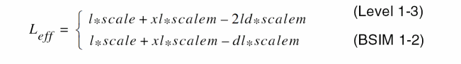
Channel Width and Length
(19-3)
(19-4)
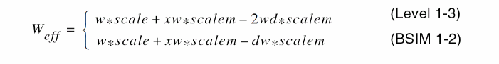
(19-5)
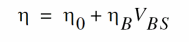
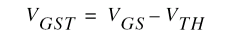
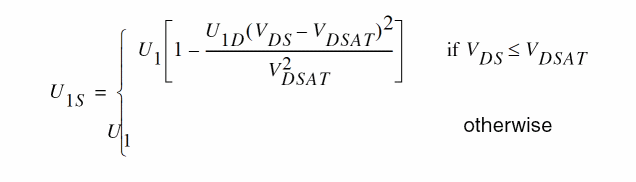
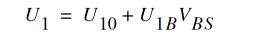
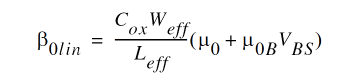
Threshold Voltage
(19-6)

where
(19-7)
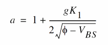
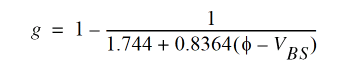
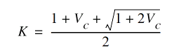
Drain Saturation Voltage
(19-8)
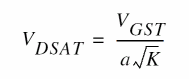
where
(19-9)
(19-10)
(19-11)
(19-12)
(19-13)
(19-14)
(19-15)
Drain Current for the Subthreshold Region
(19-16)
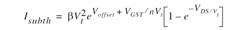
where
(19-17)
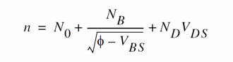
(19-18)

Drain Current for the Triode Region
(19-19)
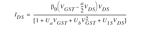
where
(19-20)
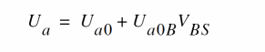
(19-21)
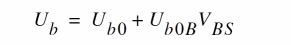
(19-22)
(19-23)
(19-24)

(19-25)
(19-26)
(19-27)

(19-28)
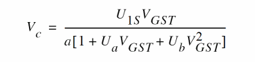
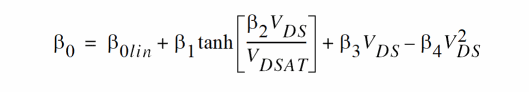
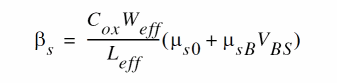
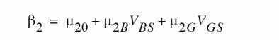
Drain Current for the Saturation Region
(19-29)
where
(19-30)
(19-31)
(19-32)
Drain Current for the Transition Region
Drain current equations are the same as those for the strong-inversion region, except that V'GST replaces all VGST terms. V'GST is calculated from a cubic spline function to match the drain current and its first derivative at the upper and lower bounds (Vghigh and Vglow).
(19-33)

All the coefficients, Cis, are automatically calculated during
(19-34)
(19-35)
(19-36)
Scaling Effects
For scaling effects, see Scaling Factors (scale and scalem).
Component Statements
This device is supported within altergroups.
Sample Instance Statement:
m2 (0 2 1 1) pchmod l=5u w=10u as=40u ad=40u pd=28u ps=28u m=1
Sample Model Statement:
model pchmod bsim2 type=p vfb0=-0.5 lvfb=0.5 wvfb=0.3 phi0=0.8 eta0=0.056 k1=0.5 eg=0.99 gap1=5.5e-04 trs=1e-3 trd=1e-3 xpart=0.5 rs=10 rd=10
Instance Syntax
Name d g s b ModelName parameter=value ...
Instance Parameters
|
w
|
(m)
|
Channel width.
|
|
l
|
(m)
|
Channel length.
|
|
as
|
(m2)
|
Area of source diffusion.
|
|
ad
|
(m2)
|
Area of drain diffusion.
|
|
ps
|
(m)
|
Perimeter of source diffusion.
|
|
pd
|
(m)
|
Perimeter of drain diffusion.
|
|
nrd
|
(m/m)
|
Number of squares of drain diffusion.
|
|
nrs
|
(m/m)
|
Number of squares of source diffusion.
|
|
ld
|
(m)
|
Drain diffusion length.
|
|
ls
|
(m)
|
Source diffusion length.
|
|
m
|
1
|
Multiplicity factor (number of MOSFETs in parallel).
|
|
region
|
triode
|
Estimated operating region. Spectre generates output number (0-4) in a rawfile.Possible values are off, triode, sat, subth and breakdown.
|
|
trise
|
(C)
|
Temperature rise from ambient.
|
|
degradation
|
no
|
Hot-electron degradation flag.Possible values are no and yes.
|
|
isnoisy
|
yes
|
Should device generate noise.Possible values are no and yes.
|
Model Syntax
model modelName bsim2 parameter=value ...
Model Parameters
Device type parameters
|
type
|
n
|
Transistor type.Possible values are n and p.
|
Threshold voltage parameters
|
vfb0
|
-0.8 V
|
Flat-band voltage.
|
|
lvfb
|
0 V μm
|
Length dependence of vfb.
|
|
wvfb
|
0 V μm
|
Width dependence of vfb.
|
|
pvfb
|
0 V μm
|
Width-length dependence of vfb.
|
|
phi0
|
0.75 V
|
Surface potential.
|
|
lphi
|
0 V μm
|
Length dependence of phi.
|
|
wphi
|
0 V μm
|
Width dependence of phi.
|
|
pphi
|
0 V μm
|
Width-length dependence of phi.
|
|
k1
|
0.7 V
|
Body-effect coefficient.
|
|
lk1
|
0 V μm
|
Length dependence of k1.
|
|
wk1
|
0 V μm
|
Width dependence of k1.
|
|
pk1
|
0 V μm
|
Width-length dependence of k1.
|
|
k2
|
0
|
Charge-sharing parameter.
|
|
lk2
|
0 μm
|
Length dependence of k2.
|
|
wk2
|
0 μm
|
Width dependence of k2.
|
|
pk2
|
0 μm
|
Width-length dependence of k2.
|
|
eta0
|
0
|
Drain-induced barrier-lowering coefficient.
|
|
leta0
|
0 μm
|
Length dependence of eta0.
|
|
weta0
|
0 μm
|
Width dependence of eta0.
|
|
peta0
|
0 μm
|
Width-length dependence of eta0.
|
|
etab
|
0 1/V
|
Body-bias dependence of eta0.
|
|
letab
|
0 μm/V
|
Length dependence of etab.
|
|
wetab
|
0 μm/V
|
Width dependence of etab.
|
|
petab
|
0 μm/V
|
Width-length dependence of etab.
|
Mobility parameters
|
mu0
|
400 cm2/V s
|
Low-field mobility.
|
|
lmu0
|
0 cm2/V s
|
Length dependence of mu0.
|
|
wmu0
|
0 cm2/V s
|
Width dependence of mu0.
|
|
pmu0
|
0 cm2/V s
|
Width-length dependence of mu0.
|
|
mu0b
|
0 cm2/V2 s
|
Body-bias dependence of muz.
|
|
lmu0b
|
0 cm2 μm/V2 s
|
Length dependence of x2mz.
|
|
wmu0b
|
0 cm2 μm/V2 s
|
Width dependence of x2mz.
|
|
pmu0b
|
0 cm2 μm/V2 s
|
Width-length dependence of x2mz.
|
|
mus0
|
450 cm2/V s
|
Mobility in the saturation region.
|
|
lmus0
|
0 cm2 μm/V s
|
Length dependence of mus0.
|
|
wmus0
|
0 cm2 μm/V s
|
Width dependence of mus0.
|
|
pmus0
|
0 cm2 μm/V s
|
Width-length dependence of mus0.
|
|
musb
|
0 cm2/V2 s
|
Body-bias dependence of mus0.
|
|
lmusb
|
0 cm2 μm/V2 s
|
Length dependence of mus0.
|
|
wmusb
|
0 cm2 μm/V2 s
|
Length dependence of mus0.
|
|
pmusb
|
0 cm2 μm/V2 s
|
Length dependence of mus0.
|
|
mu20
|
1
|
Empirical channel length modulation parameter.
|
|
lmu20
|
0 μm
|
Length dependence of mu20.
|
|
wmu20
|
0 μm
|
Width dependence of mu20.
|
|
pmu20
|
0 μm
|
Width-length dependence of mu20.
|
|
mu2b
|
0 1/V
|
Body-bias dependence of mu20.
|
|
lmu2b
|
0 μm/V
|
Length dependence of mu2b.
|
|
wmu2b
|
0 μm/V
|
Width dependence of mu2b.
|
|
pmu2b
|
0 μm/V
|
Width-length dependence of mu2b.
|
|
mu2g
|
0 1/V
|
Gate-bias dependence of mu20.
|
|
lmu2g
|
0 μm/V
|
Length dependence of mu2g.
|
|
wmu2g
|
0 μm/V
|
Width dependence of mu2g.
|
|
pmu2g
|
0 μm/V
|
Width-length dependence of mu2g.
|
|
mu30
|
5 cm2/V2 s
|
Empirical output resistance parameter.
|
|
lmu30
|
0 cm2 μm/V2 s
|
Length dependence of mu30.
|
|
wmu30
|
0 cm2 μm/V2 s
|
Width dependence of mu30.
|
|
pmu30
|
0 cm2 μm/V2 s
|
Width-length dependence of mu30.
|
|
mu3b
|
0 cm2/V3 s
|
Body-bias dependence of mu30.
|
|
lmu3b
|
0 cm2 μm/V3 s
|
Length dependence of mu3b.
|
|
wmu3b
|
0 cm2 μm/V3 s
|
Width dependence of mu3b.
|
|
pmu3b
|
0 cm2 μm/V3 s
|
Width-length dependence of mu3b.
|
|
mu3g
|
0 cm2/V3 s
|
Gate-bias dependence of mu30.
|
|
lmu3g
|
0 cm2 μm/V3 s
|
Length dependence of mu3g.
|
|
wmu3g
|
0 cm2 μm/V3 s
|
Width dependence of mu3g.
|
|
pmu3g
|
0 cm2 μm/V3 s
|
Width-length dependence of mu3g.
|
|
mu40
|
0 cm2/V3 s
|
Empirical output resistance parameter.
|
|
lmu40
|
0 cm2 μm/V3 s
|
Length dependence of mu40.
|
|
wmu40
|
0 cm2 μm/V3 s
|
Width dependence of mu40.
|
|
pmu40
|
0 cm2 μm/V3 s
|
Width-length dependence of mu40.
|
|
mu4b
|
0 cm2/V3 s
|
Empirical output resistance parameter.
|
|
lmu4b
|
0 cm2 μm/V3 s
|
Length dependence of mu4b.
|
|
wmu4b
|
0 cm2 μm/V3 s
|
Width dependence of mu4b.
|
|
pmu4b
|
0 cm2 μm/V3 s
|
Width-length dependence of mu4b.
|
|
mu4g
|
0 cm2/V3 s
|
Gate-bias dependence of mu4g.
|
|
lmu4g
|
0 cm2 μm/V3 s
|
Length dependence of mu4g.
|
|
wmu4g
|
0 cm2 μm/V3 s
|
Width dependence of mu4g.
|
|
pmu4g
|
0 cm2 μm/V3 s
|
Width-length dependence of mu4g.
|
Mobility modulation parameters
|
ua0
|
0 1/V
|
Gate voltage dependence of mobility.
|
|
lua0
|
0 μm/V
|
Length dependence of ua0.
|
|
wua0
|
0 μm/V
|
Width dependence of ua0.
|
|
pua0
|
0 μm/V
|
Width-length dependence of ua0.
|
|
uab
|
0 1/V2
|
Body-bias dependence of ua.
|
|
luab
|
0 μm/V2
|
Length dependence of uab.
|
|
wuab
|
0 μm/V2
|
Width dependence of uab.
|
|
puab
|
0 μm/V2
|
Width-length dependence of uab.
|
|
ub0
|
0 1/V2
|
Second-order effect of gate voltage dependence of mobility.
|
|
lub0
|
0 μm/V2
|
Length dependence of ub0.
|
|
wub0
|
0 μm/V2
|
Width dependence of ub0.
|
|
pub0
|
0 μm/V2
|
Width-length dependence of ub0.
|
|
ubb
|
0 1/V3
|
Body-bias dependence of ub.
|
|
lubb
|
0 μm/V3
|
Length dependence of ubb.
|
|
wubb
|
0 μm/V3
|
Width dependence of ubb.
|
|
pubb
|
0 μm/V3
|
Width-length dependence of ubb.
|
Velocity saturation parameters
|
u10
|
0 1/V
|
Velocity saturation coefficient.
|
|
lu10
|
0 μm/V
|
Length dependence of u1.
|
|
wu10
|
0 μm/V
|
Width dependence of u1.
|
|
pu10
|
0 μm/V
|
Width-length dependence of u1.
|
|
u1b
|
0 1/V2
|
Body-bias dependence of u1.
|
|
lu1b
|
0 μm/V2
|
Length dependence of u1b.
|
|
wu1b
|
0 μm/V2
|
Width dependence of u1b.
|
|
pu1b
|
0 μm/V2
|
Width-length dependence of u1b.
|
|
u1d
|
0 1/V2
|
Drain-bias dependence of u1.
|
|
lu1d
|
0 μm/V2
|
Length dependence of u1d.
|
|
wu1d
|
0 μm/V2
|
Width dependence of u1d.
|
|
pu1d
|
0 μm/V2
|
Width-length dependence of u1d.
|
Subthreshold parameters
|
n0
|
0
|
Subthreshold swing parameter.
|
|
ln0
|
0 μm
|
Length dependence of subthreshold swing parameter.
|
|
wn0
|
0 μm
|
Width dependence of subthreshold swing parameter.
|
|
pn0
|
0 μm
|
Width-length dependence of subthreshold swing parameter.
|
|
nb
|
0 V
|
Body-bias dependence of n0.
|
|
lnb
|
0 V μm
|
Length dependence of nb.
|
|
wnb
|
0 V μm
|
Width dependence of nb.
|
|
pnb
|
0 V μm
|
Width-length dependence of nb.
|
|
nd
|
0 1/V
|
Drain-bias dependence of n0.
|
|
lnd
|
0 μm/V
|
Length dependence of nd.
|
|
wnd
|
0 μm/V
|
Width dependence of nd.
|
|
pnd
|
0 μm/V
|
Width-length dependence of nd.
|
|
vof0
|
1 V
|
Threshold voltage offset in the subthreshold region.
|
|
lvof0
|
0 V μm
|
Length dependence of vof.
|
|
wvof0
|
0 V μm
|
Width dependence of vof.
|
|
pvof0
|
0 V μm
|
Width-length dependence of vof.
|
|
vofb
|
0
|
Body-bias dependence of vof0.
|
|
lvofb
|
0 μm
|
Length dependence of vofb.
|
|
wvofb
|
0 μm
|
Width dependence of vofb.
|
|
pvofb
|
0 μm
|
Width-length dependence of vofb.
|
|
vofd
|
0
|
Drain-bias dependence of vof0.
|
|
lvofd
|
0 μm
|
Length dependence of vofd.
|
|
wvofd
|
0 μm
|
Width dependence of vofd.
|
|
pvofd
|
0 μm
|
Width-length dependence of vofd.
|
|
subthmod
|
2
|
Subthreshold model selector.
|
Impact ionization parameters
|
ai0
|
0 1/V
|
Hot-electron effect on Rout parameter.
|
|
lai0
|
0 μm/V
|
Length dependence of ai0.
|
|
wai0
|
0 μm/V
|
Width dependence of ai0.
|
|
pai0
|
0 μm/V
|
Width-length dependence of ai0.
|
|
aib
|
0 1/V2
|
Body-bias dependence of ai0.
|
|
laib
|
0 μm/V2
|
Length dependence of aib.
|
|
waib
|
0 μm/V2
|
Width dependence of aib.
|
|
paib
|
0 μm/V2
|
Width-length dependence of aib.
|
|
bi0
|
0 V
|
Hot-electron effect on Rout exponent.
|
|
lbi0
|
0 V μm
|
Length dependence of bi0.
|
|
wbi0
|
0 V μm
|
Width dependence of bi0.
|
|
pbi0
|
0 V μm
|
Width-length dependence of bi0.
|
|
bib
|
0
|
Body-bias dependence of bi0.
|
|
lbib
|
0 μm
|
Length dependence of bib.
|
|
wbib
|
0 μm
|
Width dependence of bib.
|
|
pbib
|
0 μm
|
Width-length dependence of bib.
|
Transition region bound parameters
|
vghigh
|
0.2 V
|
Upper bound of the transition region.
|
|
lvghigh
|
0 V μm
|
Length dependence of Vghigh.
|
|
wvghigh
|
0 V μm
|
Width dependence of Vghigh.
|
|
pvghigh
|
0 V μm
|
Width-length dependence of Vghigh.
|
|
vglow
|
-0.15 V
|
Lower bound of the transition region.
|
|
lvglow
|
0 V μm
|
Length dependence of Vglow.
|
|
wvglow
|
0 V μm
|
Width dependence of Vglow.
|
|
pvglow
|
0 V μm
|
Width-length dependence of Vglow.
|
Length and width modulation parameters
|
dl0
|
0 μm
|
Lateral diffusion.
|
|
dw0
|
0 μm
|
Field oxide encroachment.
|
|
lref
|
infinity m
|
Reference channel length.
|
|
wref
|
infinity m
|
Reference channel width.
|
|
xw
|
0 m
|
Width variation due to masking and etching.
|
|
xl
|
0 m
|
Length variation due to masking and etching.
|
Temperature effects parameters
|
temp
|
(C)
|
Parameters measurement temperature. Default set by options.
|
|
trise
|
0 C
|
Temperature rise from ambient.
|
|
compatible
|
spectre
|
Encourage device equations to be compatible with a foreign simulator.This option does not affect the input synax.Possible values are spectre, spice2, spice3, cdsspice, hspice, spiceplus, eldo, sspice, mica, tispice and pspice.
|
|
tempmod
|
432
|
Temperature model selector.
|
|
version
|
432
|
Version selector.
|
|
uto
|
0 C
|
Mobility temperature offset.
|
|
ute
|
-1.5
|
Mobility temperature exponent.
|
|
tlev
|
0
|
DC temperature selector.
|
|
tlevc
|
0
|
AC temperature selector.
|
|
ptc
|
0 V/C
|
Surface potential temperature coefficient.
|
|
eg
|
1.12452 V
|
Energy band gap.
|
|
gap1
|
7.02e-4 V/C2
|
Band gap temperature coefficient.
|
|
gap2
|
1108 K
|
Band gap temperature offset.
|
|
trs
|
0 1/C
|
Temperature coefficient for source resistance.
|
|
trd
|
0 1/C
|
Temperature coefficient for drain resistance.
|
|
xti
|
3
|
Saturation current temperature exponent.
|
Overlap capacitance parameters
|
cgso
|
0 F/m
|
Gate-source overlap capacitance.
|
|
cgdo
|
0 F/m
|
Gate-drain overlap capacitance.
|
|
cgbo
|
0 F/m
|
Gate-bulk overlap capacitance.
|
|
meto
|
0 m
|
Metal overlap in fringing field.
|
Charge model selection parameters
|
capmod
|
bsim
|
Intrinsic charge model.Possible values are none, meyer, yang and bsim.
|
|
xpart
|
1
|
Drain/source channel charge partition in saturation for BSIM charge model, use 0.0 for 40/60, 0.5 for 50/50, or 1.0 for 0/100.
|
|
xqc
|
0
|
Drain/source channel charge partition in saturation for charge models, e.g. use 0.4 for 40/60, 0.5 for 50/50, or 0 for 0/100.
|
Parasitic resistance parameters
|
rs
|
0 Ω
|
Source resistance.
|
|
rd
|
0 Ω
|
Drain resistance.
|
|
rsh
|
0 Ω/sqr
|
Source/drain diffusion sheet resistance.
|
|
rsc
|
0 Ω
|
Source contact resistance.
|
|
rdc
|
0 Ω
|
Drain contact resistance.
|
|
rss
|
0 Ω m
|
Scalable source resistance.
|
|
rdd
|
0 Ω m
|
Scalable drain resistance.
|
|
minr
|
0.1 Ω
|
Minimum source/drain resistance.
|
|
hdif
|
0 m
|
Length of heavily doped diffusion.
|
|
ldif
|
0 m
|
Lateral diffusion beyond the gate.
|
|
lgcs
|
0 m
|
Gate-to-contact length of source side.
|
|
lgcd
|
0 m
|
Gate-to-contact length of drain side.
|
|
sc
|
infinity m
|
Spacing between contacts.
|
Junction diode parameters
|
js
|
(A/m2)
|
Bulk junction reverse saturation current density.
|
|
is
|
1e-14 A
|
Bulk junction reverse saturation current.
|
|
n
|
1
|
Junction emission coefficient.
|
|
dskip
|
yes
|
Use simple piece-wise linear model for diode currents below 0.1*iabstol.Possible values are no and yes.
|
|
imelt
|
`imaxA'
|
Explosion current, diode is linearized beyond this current to aid convergence.
|
|
jmelt
|
`jmaxA/m'2
|
Explosion current density, diode is linearized beyond this current to aid convergence.
|
Operating region warning control parameters
|
alarm
|
none
|
Forbidden operating region.Possible values are none, off, triode, sat, subth and rev.
|
|
imax
|
1 A
|
Maximum current, currents above this limit generate a warning.
|
|
jmax
|
1e8 A/m2
|
Maximum current density, currents above this limit generate a warning.
|
|
bvj
|
infinity V
|
Junction reverse breakdown voltage.
|
|
vbox
|
1e9*tox V
|
Oxide breakdown voltage.
|
Junction capacitance model parameters
|
cbs
|
0 F
|
Bulk-source zero-bias junction capacitance.
|
|
cbd
|
0 F
|
Bulk-drain zero-bias junction capacitance.
|
|
cj
|
0 F/m2
|
Zero-bias junction bottom capacitance density.
|
|
mj
|
1/2
|
Bulk junction bottom grading coefficient.
|
|
pb
|
0.8 V
|
Bulk junction potential.
|
|
fc
|
0.5
|
Forward-bias depletion capacitance threshold.
|
|
cjsw
|
0 F/m
|
Zero-bias junction sidewall capacitance density.
|
|
mjsw
|
1/3
|
Bulk junction sidewall grading coefficient.
|
|
pbsw
|
0.8 V
|
Side-wall junction potential.
|
|
fcsw
|
0.5
|
Side-wall forward-bias depletion capacitance threshold.
|
Process and power supply parameters
|
tox
|
4e-8 m
|
Gate oxide thickness.
|
|
vdd
|
5 V
|
Drain voltage at which parameters are extracted.
|
|
vgg
|
5 V
|
Gate voltage at which parameters are extracted.
|
|
vbb
|
-5 V
|
Body voltage at which parameters are extracted.
|
Default device parameters
|
w
|
3e-6 m
|
Channel width.
|
|
l
|
3e-6 m
|
Channel length.
|
|
as
|
0 m2
|
Area of source diffusion.
|
|
ad
|
0 m2
|
Area of drain diffusion.
|
|
ps
|
0 m
|
Perimeter of source diffusion.
|
|
pd
|
0 m
|
Perimeter of drain diffusion.
|
|
nrd
|
0 m/m
|
Number of squares of drain diffusion.
|
|
nrs
|
0 m/m
|
Number of squares of source diffusion.
|
|
ldd
|
0 m
|
Drain diffusion length.
|
|
lds
|
0 m
|
Source diffusion length.
|
Noise model parameters
|
noisemod
|
1
|
Noise model selector.
|
|
kf
|
0
|
Flicker (1/f) noise coefficient.
|
|
af
|
1
|
Flicker (1/f) noise exponent.
|
|
ef
|
1
|
Flicker (1/f) noise frequency exponent.
|
|
wnoi
|
1e-5 m
|
Channel width at which noise parameters were extracted.
|
Auto Model Selector parameters
|
wmax
|
1.0 m
|
Maximum channel width for which the model is valid.
|
|
wmin
|
0.0 m
|
Minimum channel width for which the model is valid.
|
|
lmax
|
1.0 m
|
Maximum channel length for which the model is valid.
|
|
lmin
|
0.0 m
|
Minimum channel length for which the model is valid.
|
Degradation parameters
|
degramod
|
spectre
|
Degradation model selector.Possible values are spectre and bert.
|
|
degradation
|
no
|
Hot-electron degradation flag.Possible values are no and yes.
|
|
dvthc
|
1 V
|
Degradation coefficient for threshold voltage.
|
|
dvthe
|
1
|
Degradation exponent for threshold voltage.
|
|
duoc
|
1 S
|
Degradation coefficient for transconductance.
|
|
duoe
|
1
|
Degradation exponent for transconductance.
|
|
crivth
|
0.1 V
|
Maximum allowable threshold voltage shift.
|
|
criuo
|
10%
|
Maximum allowable normalized mobility change.
|
|
crigm
|
10%
|
Maximum allowable normalized transconductance change.
|
|
criids
|
10%
|
Maximum allowable normalized drain current change.
|
|
wnom
|
5e-6 m
|
Nominal device width in degradation calculation.
|
|
lnom
|
1e-6 m
|
Nominal device length in degradation calculation.
|
|
vbsn
|
0 V
|
Substrate voltage in degradation calculation.
|
|
vdsni
|
0.1 V
|
Drain voltage in Ids degradation calculation.
|
|
vgsni
|
5 V
|
Gate voltage in Ids degradation calculation.
|
|
vdsng
|
0.1 V
|
Drain voltage in Gm degradation calculation.
|
|
vgsng
|
5 V
|
Gate voltage in Gm degradation calculation.
|
Spectre stress parameters
|
esat
|
1.1e7 V/m
|
Critical field in Vdsat calculation.
|
|
esatg
|
2.5e6 1/m
|
Gate voltage dependence of esat.
|
|
vpg
|
-0.25
|
Gate voltage modifier.
|
|
vpb
|
-0.13
|
Gate voltage modifier.
|
|
subc1
|
2.24e-5
|
Substrate current coefficient.
|
|
subc2
|
-0.1e-5 1/V
|
Substrate current coefficient.
|
|
sube
|
6.4
|
Substrate current exponent.
|
|
strc
|
1
|
Stress coefficient.
|
|
stre
|
1
|
Stress exponent.
|
BERT stress parameters
|
h0
|
1
|
Aging coefficient.
|
|
hgd
|
0 1/V
|
Bias dependence of h0.
|
|
m0
|
1
|
Aging exponent.
|
|
mgd
|
0 1/V
|
Bias dependence of m0.
|
|
ecrit0
|
1.1e5 V/cm
|
Critical electric field.
|
|
lecrit0
|
0 μm V/cm
|
Length dependence of ecrit0.
|
|
wecrit0
|
0 μm V/cm
|
Width dependence of ecrit0.
|
|
ecritg
|
0 1/cm
|
Gate voltage dependence of ecrit0.
|
|
lecritg
|
0 μm/cm
|
Length dependence of ecritg.
|
|
wecritg
|
0 μm/cm
|
Width dependence of ecritg.
|
|
ecritb
|
0 1/cm
|
Substrate voltage dependence of ecrit0.
|
|
lecritb
|
0 μm/cm
|
Length dependence of ecritb.
|
|
wecritb
|
0 μm/cm
|
Width dependence of ecritb.
|
|
lc0
|
1
|
Substrate current coefficient.
|
|
llc0
|
0 μm
|
Length dependence of lc0.
|
|
wlc0
|
0 μm
|
Width dependence of lc0.
|
|
lc1
|
1
|
Substrate current coefficient.
|
|
llc1
|
0 μm
|
Length dependence of lc1.
|
|
wlc1
|
0 μm
|
Width dependence of lc1.
|
|
lc2
|
1
|
Substrate current coefficient.
|
|
llc2
|
0 μm
|
Length dependence of lc2.
|
|
wlc2
|
0 μm
|
Width dependence of lc2.
|
|
lc3
|
1
|
Substrate current coefficient.
|
|
llc3
|
0 μm
|
Length dependence of lc3.
|
|
wlc3
|
0 μm
|
Width dependence of lc3.
|
|
lc4
|
1
|
Substrate current coefficient.
|
|
llc4
|
0 μm
|
Length dependence of lc4.
|
|
wlc4
|
0 μm
|
Width dependence of lc4.
|
|
lc5
|
1
|
Substrate current coefficient.
|
|
llc5
|
0 μm
|
Length dependence of lc5.
|
|
wlc5
|
0 μm
|
Width dependence of lc5.
|
|
lc6
|
1
|
Substrate current coefficient.
|
|
llc6
|
0 μm
|
Length dependence of lc6.
|
|
wlc6
|
0 μm
|
Width dependence of lc6.
|
|
lc7
|
1
|
Substrate current coefficient.
|
|
llc7
|
0 μm
|
Length dependence of lc7.
|
|
wlc7
|
0 μm
|
Width dependence of lc7.
|
Imax and Imelt:
The imax parameter aids convergence and prevents numerical overflow. The junction characteristics of the device are accurately modeled for current up to imax. If imax is exceeded during iterations, the linear model is substituted until the current drops below imax or until convergence is achieved. If convergence is achieved with the current exceeding imax, the results are inaccurate, and Spectre prints a warning.
A separate model parameter, imelt, is used as a limit warning for the junction current. This parameter can be set to the maximum current rating of the device. When any component of the junction current exceeds imelt, the base and collector currents are composed of many exponential terms, Spectre issues a warning and the results become inaccurate. The junction current is linearized above the value of imelt to prevent arithmetic exception, with the exponential term replaced by a linear equation at imelt.
Both of these parameters have current density counterparts, jmax and jmelt, that you can specify if you want the absolute current values to depend on the device area.
Auto Model Selection:
Many models need to be characterized for different geometries in order to obtain accurate results for model development. The model selector program automatically searches for a model with the length and width range specified in the instance statement and uses this model in the simulations.
For the auto model selector program to find a specific model, the models to be searched should be grouped together within braces. Such a group is called a model group. An opening brace is required at the end of the line defining each model group. Every model in the group is given a name followed by a colon and the list of parameters. Also, the four geometric parameters lmax, lmin, wmax, and wmin should be given. The selection criteria to choose a model is as follows:
lmin <= inst_length < lmax and wmin <= inst_width < wmax
Example:
model ModelName ModelType {
1: <model parameters> lmin=2 lmax=4 wmin=1 wmax=2
2: <model parameters> lmin=1 lmax=2 wmin=2 wmax=4
3: <model parameters> lmin=2 lmax=4 wmin=4 wmax=6
}
Then for a given instance
M1 1 2 3 4 ModelName w=3 l=1.5
the program would search all the models in the model group with the name ModelName and then pick the first model whose geometric range satisfies the selection criteria. In the preceding example, the auto model selector program would choose ModelName.2.
You must specify both length (l) and width (w) on the device instance line to enable automatic model selection.
Output Parameters
|
tempeff
|
(C)
|
Effective temperature for a single device.
|
|
weff
|
(m)
|
Effective channel width.
|
|
leff
|
(m)
|
Effective channel length.
|
|
rseff
|
(Ω)
|
Effective source resistance.
|
|
rdeff
|
(Ω)
|
Effective drain resistance.
|
|
aseff
|
(m2)
|
Effective area of source diffusion.
|
|
adeff
|
(m2)
|
Effective area of drain diffusion.
|
|
pseff
|
(m)
|
Effective perimeter of source diffusion.
|
|
pdeff
|
(m)
|
Effective perimeter of source diffusion.
|
|
isseff
|
(A)
|
Effective source-bulk junction reverse saturation current.
|
|
isdeff
|
(A)
|
Effective drain-bulk junction reverse saturation current.
|
|
cbseff
|
(F)
|
Effective zero-bias source-bulk junction capacitance.
|
|
cbdeff
|
(F)
|
Effective zero-bias drain-bulk junction capacitance.
|
|
vto
|
(V)
|
Effective zero-bias threshold voltage.
|
|
vfb
|
(V)
|
Effective flat-band voltage.
|
|
phi
|
(V)
|
Effective surface potential.
|
|
k1
|
(V )
|
Effective body-effect coefficient.
|
|
k2
|
|
Effective charge-sharing parameter.
|
|
eta
|
|
Effective DIBL coefficient.
|
Related Topics
MOS Level-2 Model (mos2)
MOS Level-3 Model (mos3)
BSIM1 Level-4 Model (bsim1)
BSIM3v2 Level-10 Model (bsim3)
Return to top