16
MOS Level-2 Model (mos2)
The MOS2 model is the level-2 model from Berkeley SPICE. The MOS2 model is an analytical, one-dimensional model that incorporates most of the second-order small-size effects. A smoother version of the level-2 model (with continuous Gds at Vdsat) as well as three charge models are also available. Click to view the following links for information about the MOS2 model:
Channel Width and Length
(16-1)
(16-2)
(16-3)
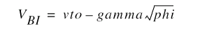
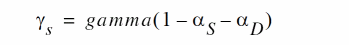
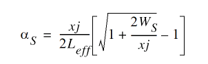
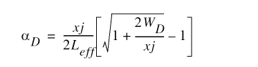
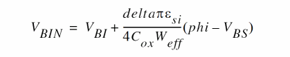
Threshold Voltage
(16-4)

where
(16-5)
(16-6)
(16-7)
(16-8)
(16-9)
(16-10)
(16-11)
(16-12)
If xj or nsub is zero, the short-channel effects on threshold voltage are not evaluated (that is, γs = gamma).
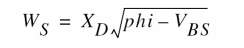
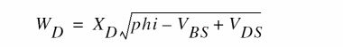
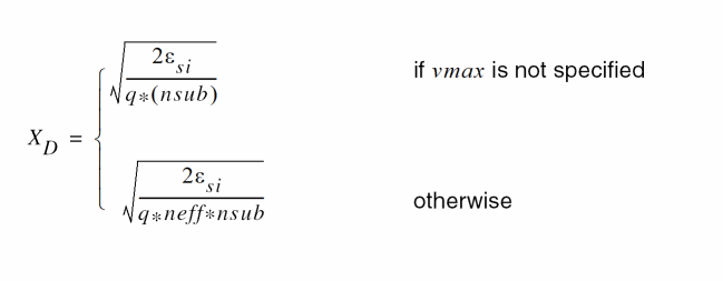
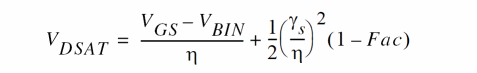
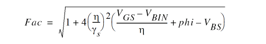
Drain Saturation Voltage
If vmax is not specified, VDSAT is determined by the pinchoff condition and is given by
(16-13)
where
(16-14)
(16-15)
If vmax is specified, VDSAT is determined by the velocity saturation effect.
(16-16)
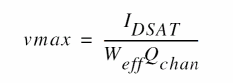
where
(16-17)

μeff is the effective mobility, defined later. VDSAT can be calculated by solving the preceding equations.
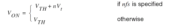
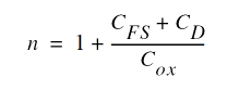
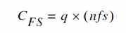
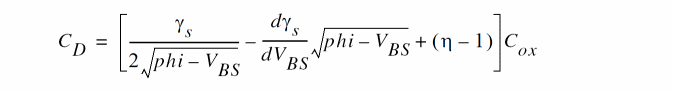
Drain Current for the Subthreshold Region
You cannot use the subthreshold current equations without nfs.
(16-18)
where
(16-19)
(16-20)
(16-21)
(16-22)
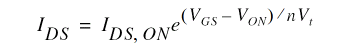
where IDS,ON is the drain current evaluated at VGS = VON.
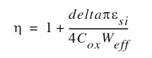
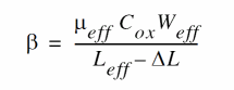
Drain Current for the Triode Region
(16-23)

where
(16-24)
(16-25)
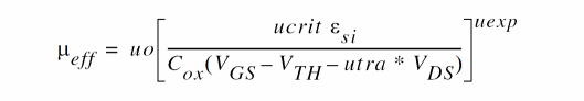
SPICE does not implement the utra effect. Also, if (VGS –VTH) ≤ (ucritεsi/Cox), μeff is clipped to uo. This creates a discontinuity in the first derivatives of the drain current. The Spectre® circuit simulator does not have this clipping effect.
(16-26)
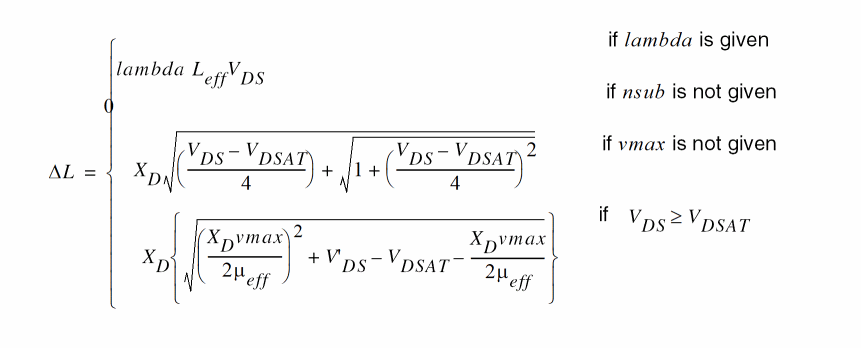
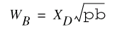
If ΔL ≥ (Leff – WB), β is calculated from the following equation to avoid device punch-through:
(16-27)
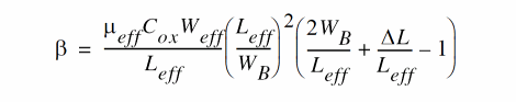
where
(16-28)
Drain Current for the Saturation Region
(16-29)

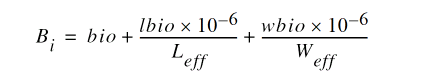
Substrate Current
The substrate current results from impact ionization in the velocity saturation region near the drain. This impact-ionization induced current (IDB) flows between the drain and the substrate. You need both aio and bio to use the impact-ionization model.
(16-30)
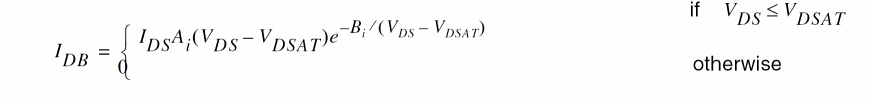
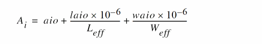
where
(16-31)
(16-32)
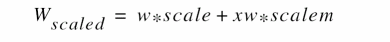
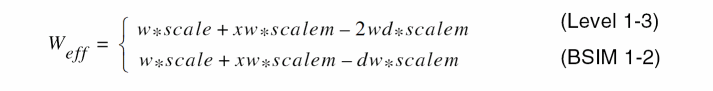
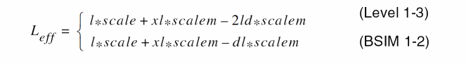
Scaling Effects
For scaling effects, see Scaling Factors (scale and scalem).
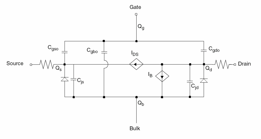
Component Statements
This device is supported within altergroups.
Sample Instance Statement
mn2 (1 2 0 0) nch2 w=10u ad=20p as=20p ps=24u pd=24u
Sample Model Statement
model nch2 mos2 type=n vto=0.66 lambda=0.018 gamma=0.6 nsub=0.213e16 kp=0.978e-4 tpg=-1 vmax=6e4 ucrit=1e7 utra=0.1 uexp=0.2 is=0
Instance Syntax
Name d g s b ModelName parameter=value ...
Instance Parameters
|
w (m)
|
Channel width.
|
|
l (m)
|
Channel length.
|
|
as (m2)
|
Area of source diffusion.
|
|
ad (m2)
|
Area of drain diffusion.
|
|
ps (m)
|
Perimeter of source diffusion.
|
|
pd (m)
|
Perimeter of drain diffusion.
|
|
nrd (m/m)
|
Number of squares of drain diffusion.
|
|
nrs (m/m)
|
Number of squares of source diffusion.
|
|
ld (m)
|
Length of drain diffusion region.
|
|
ls (m)
|
Length of source diffusion region.
|
|
m=1
|
Multiplicity factor (number of MOSFETs in parallel).
|
|
region=triode
|
Estimated operating region. Spectre generates output number (0-4) in a rawfile. Possible values are off, triode, sat, subth, or breakdown.
|
|
trise
|
Temperature rise from ambient.
|
|
isnoisy=yes
|
Should resistor generate noise. Possible values are no or yes.
|
|
degradation=no
|
Hot-electron degradation flag. Possible values are no or yes.
|
Model Definition
model modelName mos2 parameter=value ...
Model Parameters
Device type parameters
|
type=n
|
Transistor type. Possible values are n or p.
|
Drain current model parameters
|
vto=0 V
|
Threshold voltage at zero body bias.
|
|
kp=2.0718e-5 A/V2
|
|
|
|
Transconductance parameter.
|
|
lambda=0 1/V
|
Channel length modulation parameter.
|
|
phi=0.7 V
|
Surface potential at strong inversion.
|
|
gamma=0 √V
|
Body-effect parameter.
|
|
uo=600 cm2/V s
|
Carrier surface mobility.
|
|
vmax=0.0 m/s
|
Carrier saturation velocity.
|
|
ucrit=0 V/cm
|
Critical field for mobility degradation.
|
|
uexp=0
|
Critical field exponent for mobility degradation.
|
|
utra=0 1/V
|
Transverse field for mobility.
|
|
neff=1
|
Total channel charge coefficient.
|
|
delta=0
|
Width effect on threshold voltage.
|
|
smooth=yes
|
Drain current smoothing flag. Possible values are no or yes.
|
Process parameters
|
nsub=1.13e16 cm-3
|
|
|
|
Channel doping concentration.
|
|
nss=0 cm-2
|
Surface state density.
|
|
nfs=0 cm-2
|
Fast surface state density.
|
|
tpg=+1
|
Type of gate (+1 = opposite of substrate, -1 = same as substrate, 0 = aluminum).
|
|
tox=1e-7 m
|
Gate oxide thickness.
|
|
ld=0 m
|
Lateral diffusion.
|
|
wd=0 m
|
Field-oxide encroachment.
|
|
xw=0 m
|
Width variation due to masking and etching.
|
|
xl=0 m
|
Length variation due to masking and etching.
|
|
xj=0 m
|
Source/drain junction depth.
|
Impact ionization parameters
|
ai0=0 1/V
|
Impact ionization current coefficient.
|
|
lai0=0 μm/V
|
Length sensitivity of ai0.
|
|
wai0=0 μm/V
|
Width sensitivity of ai0.
|
|
bi0=0 V
|
Impact ionization current exponent.
|
|
lbi0=0 μm V
|
Length sensitivity of bi0.
|
|
wbi0=0 μm V
|
Width sensitivity of bi0.
|
Overlap capacitance parameters
|
cgso=0 F/m
|
Gate-source overlap capacitance.
|
|
cgdo=0 F/m
|
Gate-drain overlap capacitance.
|
|
cgbo=0 F/m
|
Gate-bulk overlap capacitance.
|
|
meto=0 m
|
Metal overlap in fringing field.
|
Charge model selection parameters
|
capmod=bsim
|
Intrinsic charge model. Possible values are none, meyer, yang, or bsim.
|
|
xpart=1
|
Drain/source channel charge partition in saturation for BSIM charge model, use 0.0 for 40/60, 0.5 for 50/50, or 1.0 for 0/100.
|
|
xqc=0
|
Drain/source channel charge partition in saturation for charge models, e.g. use 0.4 for 40/60, 0.5 for 50/50, 0 for 0/100.
|
Parasitic resistance parameters
|
rs=0 Ω
|
Source resistance.
|
|
rd=0 Ω
|
Drain resistance.
|
|
rsh=0 Ω/sqr
|
Source/drain diffusion sheet resistance.
|
|
rss=0 Ω m
|
Scalable source resistance.
|
|
rdd=0 Ω m
|
Scalable drain resistance.
|
|
rsc=0 Ω
|
Source contact resistance.
|
|
rdc=0 Ω
|
Drain contact resistance.
|
|
minr=0.1 Ω
|
Minimum source/drain resistance.
|
|
ldif=0 m
|
Lateral diffusion beyond the gate.
|
|
hdif=0 m
|
Length of heavily doped diffusion.
|
|
lgcs=0 m
|
Gate-to-contact length of source side.
|
|
lgcd=0 m
|
Gate-to-contact length of drain side.
|
|
sc=∞ m
|
Spacing between contacts.
|
Junction diode model parameters
|
js (A/m2)
|
Bulk junction reverse saturation current density.
|
|
is=1e-14 A
|
Bulk junction reverse saturation current.
|
|
n=1
|
Junction emission coefficient.
|
|
dskip=yes
|
Use simple piece-wise linear model for diode currents below 0.1*iabstol. Possible values are no or yes.
|
|
imelt=`imax' A
|
Explosion current, diode is linearized beyond this current to aid convergence.
|
|
jmelt=`jmax' A/m'2
|
|
|
|
Explosion current density, diode is linearized beyond this current to aid convergence.
|
Junction capacitance model parameters
|
cbs=0 F
|
Bulk-source zero-bias junction capacitance.
|
|
cbd=0 F
|
Bulk-drain zero-bias junction capacitance.
|
|
cj=0 F/m2
|
Zero-bias junction bottom capacitance density.
|
|
mj=1/2
|
Bulk junction bottom grading coefficient.
|
|
pb=0.8 V
|
Bulk junction built-in potential.
|
|
fc=0.5
|
Forward-bias depletion capacitance threshold.
|
|
cjsw=0 F/m
|
Zero-bias junction sidewall capacitance density.
|
|
mjsw=1/3
|
Bulk junction sidewall grading coefficient.
|
|
pbsw=0.8 V
|
Side-wall junction built-in potential.
|
|
fcsw=0.5
|
Side-wall forward-bias depletion capacitance threshold.
|
Operating region warning control parameters
|
alarm=none
|
Forbidden operating region. Possible values are none, off, triode, sat, subth, or rev.
|
|
imax=1 A
|
Maximum current, currents above this limit generate a warning.
|
|
jmax=1e8 A/m2
|
Maximum current density, currents above this limit generate a warning.
|
|
bvj=∞ V
|
Junction reverse breakdown voltage.
|
|
vbox=1e9 tox V
|
Oxide breakdown voltage.
|
Temperature effects parameters
|
tnom (C)
|
Parameters measurement temperature. Default set by options.
|
|
trise=0 C
|
Temperature rise from ambient.
|
|
uto=0 C
|
Mobility temperature offset.
|
|
ute=-1.5
|
Mobility temperature exponent.
|
|
tlev=0
|
DC temperature selector.
|
|
tlevc=0
|
AC temperature selector.
|
|
eg=1.12452 V
|
Energy band gap.
|
|
gap1=7.02e-4 V/C
|
Band gap temperature coefficient.
|
|
gap2=1108 C
|
Band gap temperature offset.
|
|
f1ex=0
|
Temperature exponent for ucrit.
|
|
lamex=0 1/C
|
Temperature parameter for lambda and kappa.
|
|
trs=0 1/C
|
Temperature parameter for source resistance.
|
|
trd=0 1/C
|
Temperature parameter for drain resistance.
|
|
xti=3
|
Saturation current temperature exponent.
|
|
ptc=0 V/C
|
Surface potential temperature coefficient.
|
|
tcv=0 V/C
|
Threshold voltage temperature coefficient.
|
|
pta=0 V/C
|
Junction potential temperature coefficient.
|
|
ptp=0 V/C
|
Sidewall junction potential temperature coefficient.
|
|
cta=0 1/C
|
Junction capacitance temperature coefficient.
|
|
ctp=0 1/C
|
Sidewall junction capacitance temperature coefficient.
|
Default instance parameters
|
w=3e-6 m
|
Default channel width.
|
|
l=3e-6 m
|
Default channel length.
|
|
as=0 m2
|
Default area of source diffusion.
|
|
ad=0 m2
|
Default area of drain diffusion.
|
|
ps=0 m
|
Default perimeter of source diffusion.
|
|
pd=0 m
|
Default perimeter of drain diffusion.
|
|
nrd=0 m/m
|
Default number of squares of drain diffusion.
|
|
nrs=0 m/m
|
Default number of squares of source diffusion.
|
|
ldd=0 m
|
Default length of drain diffusion region.
|
|
lds=0 m
|
Default length of source diffusion region.
|
Noise model parameters
|
noisemod=1
|
Noise model selector.
|
|
kf=0
|
Flicker (1/f) noise coefficient.
|
|
af=1
|
Flicker (1/f) noise exponent.
|
|
ef=1
|
Flicker (1/f) noise frequency exponent.
|
|
wnoi=1e-5 m
|
Channel width at which noise parameters were extracted.
|
Auto Model Selector parameters
|
wmax=1.0 m
|
Maximum channel width for which the model is valid.
|
|
wmin=0.0 m
|
Minimum channel width for which the model is valid.
|
|
lmax=1.0 m
|
Maximum channel length for which the model is valid.
|
|
lmin=0.0 m
|
Minimum channel length for which the model is valid.
|
Degradation parameters
|
degramod=spectre
|
Degradation model selector. Possible values are spectre or bert.
|
|
degradation=no
|
Hot-electron degradation flag. Possible values are no or yes.
|
|
dvthc=1 V
|
Degradation coefficient for threshold voltage.
|
|
dvthe=1
|
Degradation exponent for threshold voltage.
|
|
duoc=1 S
|
Degradation coefficient for transconductance.
|
|
duoe=1
|
Degradation exponent for transconductance.
|
|
crivth=0.1 V
|
Maximum allowable threshold voltage shift.
|
|
criuo=10%
|
Maximum allowable normalized mobility change.
|
|
crigm=10%
|
Maximum allowable normalized transconductance change.
|
|
criids=10%
|
Maximum allowable normalized drain current change.
|
|
wnom=5e-6 m
|
Nominal device width in degradation calculation.
|
|
lnom=1e-6 m
|
Nominal device length in degradation calculation.
|
|
vbsn=0 V
|
Substrate voltage in degradation calculation.
|
|
vdsni=0.1 V
|
Drain voltage in Ids degradation calculation.
|
|
vgsni=5 V
|
Gate voltage in Ids degradation calculation.
|
|
vdsng=0.1 V
|
Drain voltage in Gm degradation calculation.
|
|
vgsng=5 V
|
Gate voltage in Gm degradation calculation.
|
Spectre stress parameters
|
esat=1.1e7 V/m
|
Critical field in Vdsat calculation.
|
|
esatg=2.5e6 1/m
|
Gate voltage dependence of esat.
|
|
vpg=-0.25
|
Gate voltage modifier.
|
|
vpb=-0.13
|
Gate voltage modifier.
|
|
subc1=2.24e-5
|
Substrate current coefficient.
|
|
subc2=-0.1e-5 1/V
|
Substrate current coefficient.
|
|
sube=6.4
|
Substrate current exponent.
|
|
strc=1
|
Stress coefficient.
|
|
stre=1
|
Stress exponent.
|
BERT stress parameters
|
h0=1
|
Aging coefficient.
|
|
hgd=0 1/V
|
Bias dependence of h0.
|
|
m0=1
|
Aging exponent.
|
|
mgd=0 1/V
|
Bias dependence of m0.
|
|
ecrit0=1.1e5 V/cm
|
Critical electric field.
|
|
lecrit0=0 μm V/cm
|
Length dependence of ecrit0.
|
|
wecrit0=0 μm V/cm
|
Width dependence of ecrit0.
|
|
ecritg=0 1/cm
|
Gate voltage dependence of ecrit0.
|
|
lecritg=0 μm/cm
|
Length dependence of ecritg.
|
|
wecritg=0 μm/cm
|
Width dependence of ecritg.
|
|
ecritb=0 1/cm
|
Substrate voltage dependence of ecrit0.
|
|
lecritb=0 μm/cm
|
Length dependence of ecritb.
|
|
wecritb=0 μm/cm
|
Width dependence of ecritb.
|
|
lc0=1
|
Substrate current coefficient.
|
|
llc0=0 μm
|
Length dependence of lc0.
|
|
wlc0=0 μm
|
Width dependence of lc0.
|
|
lc1=1
|
Substrate current coefficient.
|
|
llc1=0 μm
|
Length dependence of lc1.
|
|
wlc1=0 μm
|
Width dependence of lc1.
|
|
lc2=1
|
Substrate current coefficient.
|
|
llc2=0 μm
|
Length dependence of lc2.
|
|
wlc2=0 μm
|
Width dependence of lc2.
|
|
lc3=1
|
Substrate current coefficient.
|
|
llc3=0 μm
|
Length dependence of lc3.
|
|
wlc3=0 μm
|
Width dependence of lc3.
|
|
lc4=1
|
Substrate current coefficient.
|
|
llc4=0 μm
|
Length dependence of lc4.
|
|
wlc4=0 μm
|
Width dependence of lc4.
|
|
lc5=1
|
Substrate current coefficient.
|
|
llc5=0 μm
|
Length dependence of lc5.
|
|
wlc5=0 μm
|
Width dependence of lc5.
|
|
lc6=1
|
Substrate current coefficient.
|
|
llc6=0 μm
|
Length dependence of lc6.
|
|
wlc6=0 μm
|
Width dependence of lc6.
|
|
lc7=1
|
Substrate current coefficient.
|
|
llc7=0 μm
|
Length dependence of lc7.
|
|
wlc7=0 μm
|
Width dependence of lc7.
|
Shrink Parameters
Imax and Imelt
The imax parameter aids convergence and prevents numerical overflow. The junction characteristics of the device are accurately modeled for current up to imax. If imax is exceeded during iterations, the linear model is substituted until the current drops below imax or until convergence is achieved. If convergence is achieved with the current exceeding imax, the results are inaccurate, and Spectre prints a warning.
A separate model parameter, imelt, is used as a limit warning for the junction current. This parameter can be set to the maximum current rating of the device. When any component of the junction current exceeds imelt, the base and collector currents are composed of many exponential terms, Spectre issues a warning and the results become inaccurate. The junction current is linearized above the value of imelt to prevent arithmetic exception, with the exponential term replaced by a linear equation at imelt.
Both of these parameters have current density counterparts, jmax and jmelt, that you can specify if you want the absolute current values to depend on the device area.
Auto Model Selection
Many models need to be characterized for different geometries in order to obtain accurate results for model development. The model selector program automatically searches for a model with the length and width range specified in the instance statement and uses this model in the simulations.
For the auto model selector program to find a specific model, the models to be searched should be grouped together within braces. Such a group is called a model group. An opening brace is required at the end of the line defining each model group. Every model in the group is given a name followed by a colon and the list of parameters. Also, the four geometric parameters lmax, lmin, wmax, and wmin should be given. The selection criteria to choose a model is as follows:
lmin <= inst_length < lmax and wmin <= inst_width < wmax
Example:
model ModelName ModelType {
1: <model parameters> lmin=2 lmax=4 wmin=1 wmax=2
2: <model parameters> lmin=1 lmax=2 wmin=2 wmax=4
3: <model parameters> lmin=2 lmax=4 wmin=4 wmax=6
}
Then for a given instance
M1 1 2 3 4 ModelName w=3 l=1.5
the program would search all the models in the model group with the name ModelName and then pick the first model whose geometric range satisfies the selection criteria. In the preceding example, the auto model selector program would choose ModelName.2.
You must specify both length (l) and width (w) on the device instance line to enable automatic model selection.
Output Parameters
|
tempeff (C)
|
Effective temperature for a single device.
|
|
meff
|
Effective multiplicity factor (m-factor).
|
|
weff (m)
|
Effective channel width.
|
|
leff (m)
|
Effective channel length.
|
|
rseff (Ω)
|
Effective source resistance.
|
|
rdeff (Ω)
|
Effective drain resistance.
|
|
aseff (m2)
|
Effective area of source diffusion.
|
|
adeff (m2)
|
Effective area of drain diffusion.
|
|
pseff (m)
|
Effective perimeter of source diffusion.
|
|
pdeff (m)
|
Effective perimeter of source diffusion.
|
|
isseff (A)
|
Effective source-bulk junction reverse saturation current.
|
|
isdeff (A)
|
Effective drain-bulk junction reverse saturation current.
|
|
cbseff (F)
|
Effective zero-bias source-bulk junction capacitance.
|
|
cbdeff (F)
|
Effective zero-bias drain-bulk junction capacitance.
|
Operating-Point Parameters
|
type=n
|
Transistor type. Possible values are n or p.
|
|
region=triode
|
Estimated operating region. Spectre generates output number (0-4) in a rawfile. Possible values are off, triode, sat, subth, or breakdown.
|
|
trise (C)
|
Temperature rise from ambient.
|
|
degradation=no
|
Hot-electron degradation flag. Possible values are no or yes.
|
|
reversed
|
Reverse mode indicator. Possible values are no or yes.
|
|
ids (A)
|
Resistive drain-to-source current.
|
|
vgs (V)
|
Gate-source voltage.
|
|
vds (V)
|
Drain-source voltage.
|
|
vbs (V)
|
Bulk-source voltage.
|
|
vth (V)
|
Threshold voltage.
|
|
vdsat (V)
|
Drain-source saturation voltage.
|
|
gm (S)
|
Common-source transconductance.
|
|
gds (S)
|
Common-source output conductance.
|
|
gmbs (S)
|
Body-transconductance.
|
|
gameff (√V )
|
Effective body effect coefficient.
|
|
betaeff (A/V2)
|
Effective beta.
|
|
cbd (F)
|
Drain-bulk junction capacitance.
|
|
cbs (F)
|
Source-bulk junction capacitance.
|
|
cgs (F)
|
Gate-source capacitance.
|
|
cgd (F)
|
Gate-drain capacitance.
|
|
cgb (F)
|
Gate-bulk capacitance.
|
|
ron (Ω)
|
On-resistance.
|
|
id (A)
|
Resistive drain current.
|
|
ibulk (A)
|
Resistive bulk current.
|
|
pwr (W)
|
Power at op point.
|
|
gmoverid (1/V)
|
Gm/Ids.
|
|
isub (A)
|
Substrate current.
|
|
stress
|
Hot-electron stress.
|
|
age (s)
|
Device age.
|
|
he_vdsat (V)
|
Hot Electron Vdsat.
|
Related Topics
MOS Level-3 Model (mos3)
BSIM1 Level-4 Model (bsim1)
BSIM2 Level-5 Model (bsim2)
BSIM3v2 Level-10 Model (bsim3)
Return to top