Reference
Model Equations
Some important model equations are listed as following for your reference:
Basic Equations Solved in the HiSIM SOI Core Part
Though all following descriptions are written for the n-channel MOSFET, they are also valid for the p-channel case. The Poisson equation solved in HiSIM SOI together with the Gauss law and boundary conditions together with the approximation of the linearly decreasing carrier density to the depth direction are
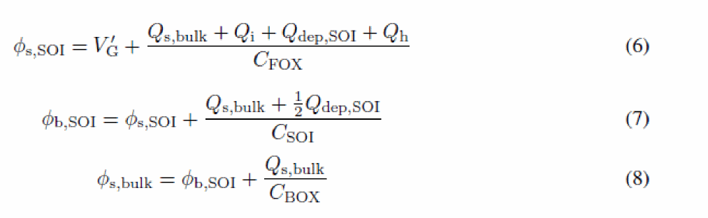
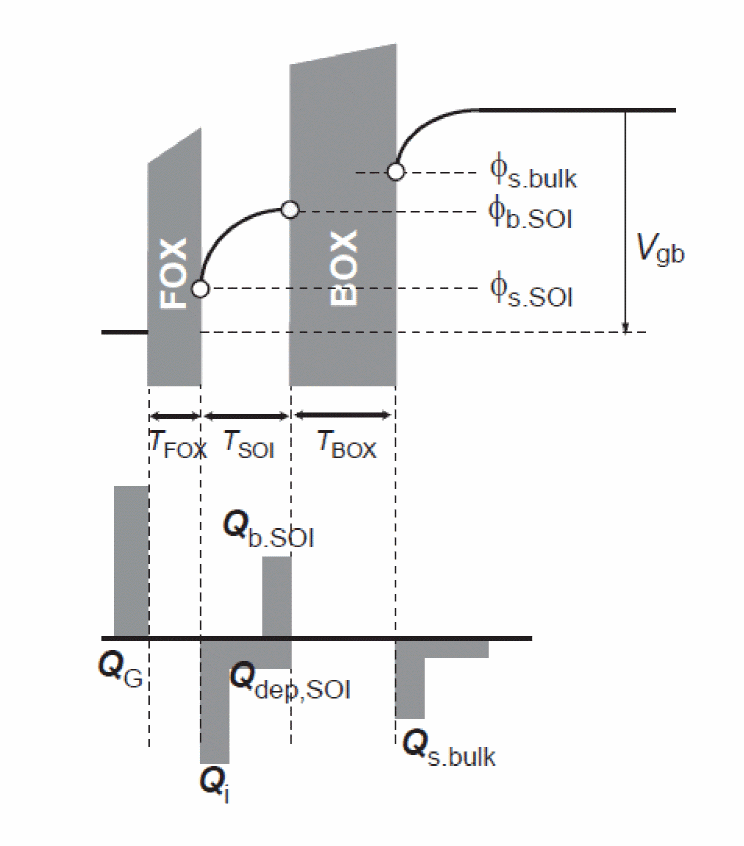
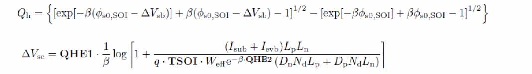
where Q’s are charges induced within the SOI-MOSFET as depicted in 32-4 and Qh is the excess charge in the SOI layer due to the impact ionization, and
where VFBC is the flat-band voltage, TFOX is the physical gate-oxide thickness, and  is the threshold voltage shift in comparison to the threshold voltage of a long-channel transistor [4].
 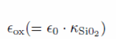 is the permittivity of Si02.
  are the permittivity of vacuum and the dielectric constant of SiO2, respectively.
Eqs. (6)– (8) are solved simultaneously within HiSIM SOI. For the body-tied case, the potential node  is connected to the external node potential and solved by the circuit simulator. The solution takes place at source side and drain side. Prior to the Newton iteration, an approximated, analytical initial value for each variable is estimated in the code.
Figure -4
Band structure of SOI-MOSFET and generated charges
All device characteristics are determined on the basis of the charge control by applied voltages. All charges induced within SOI-MOSFET are functions of surface potentials written as
Drain Current
Under the gradual-channel approximation with further approximations of an idealized gate structure and uniform channel doping, the drain current Ids is written as:
Threshold Voltage Shift
The surface-potential-based model requires no threshold voltage Vth in its core description of the model. However, HiSIM SOI has opted for modeling various submodels such as short-channel effects as a Vth shift from an otherwise ideal case.
The whole contribution to the Vth is summarised as
 Vth =
Vth =  Vth, SC +
  Vth,R +
  Vth,P +
  Vth,SCR +
  Vth,W +
  Vth,sm -
  Spg
Spg
The modeled Vth is incorporated in the  S iteration can be viewed as consisting of two main effects or components:
(I) the short-channel effect:  Vth, SC
(II) the reverse-short-channel effect:  Vth, R and
  Vth, P
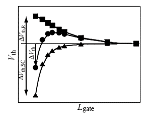
The separation into these two components ( Vth =
Vth =  Vth, SC +
  Vth, R (or
  Vth, P)) is schematically shown in Figure 32-5.
Figure -5
Schematic plot of the separation of Vth into the contributions of the short-channel and the reverse short-channel effect.
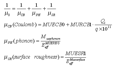
Mobility Model
The low-field mobility is described with the following expressions and includes the three independent mechanisms of Coulomb, phonon and surface-roughness scattering:
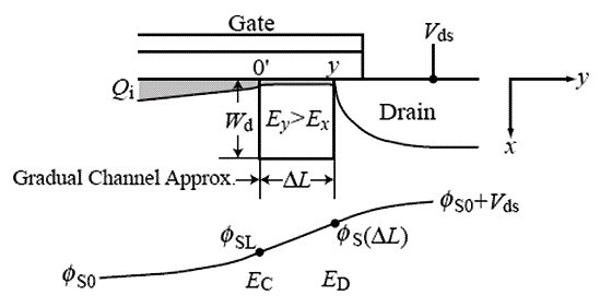
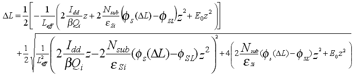
Channel-Length Modulation
As the gradual-channel approximation is not valid for large Vds causing the pinch-off phenomenon in the channel. Without taking into account the pinch-off phenomenon, the calculated channel conductance gds enters abruptly into the saturation condition. To include the pinch-off phenomenon in HiSIM, we apply the conventional method of modeling the pinch-off region ( L) separately from the rest of the channel as depicted in Figure 32-6:
Figure -6
Schematic showing the correlation among physical quantities in the pinch-off region.
After taking into all effects, the final  L is derived as:
Narrow-Channel Effects
The Vth reduction for reduced channel width (Wgate) is modeled under inclusion of the edge-fringing capacitances Cef at the edge of the trench as:
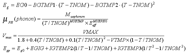
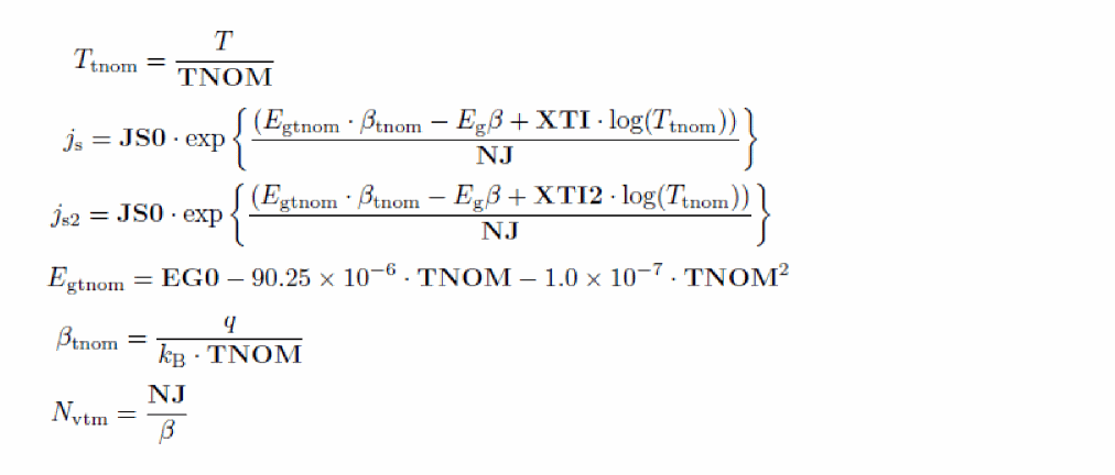
Temperature Dependences
The temperature dependence is included automatically in the surface potentials through  , which is the inverse of the thermal voltage. Additionally the band gap, the intrinsic carrier concentration, the carrier mobility, and the carrier saturation velocity are also temperature dependent.
Drain-side resistance
Source-side resistance
Gate resistance
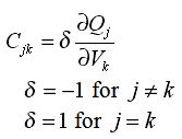
Capacitance
Intrinsic Capacitance
The intrinsic capacitances are derivatives of the node charges determined as
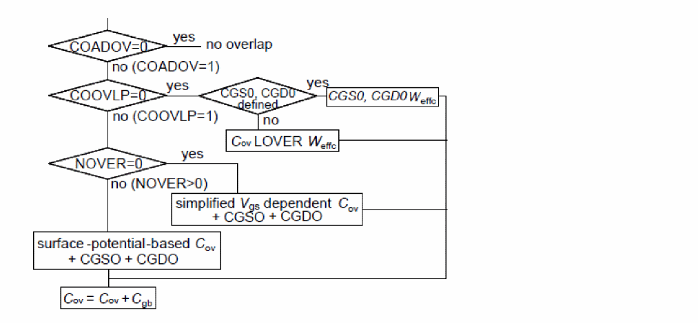
Overlap Capacitance
To consider the overlap capacitance, the flag COADOV must be selected to 1, which is the default. The overlap capacitance includes three options as summarized in 32-7, where the drain side and the source side are treated as identical. If Flag COOVLP=0, the overlap capacitances are treated to be constant. If CGSO and CGDO are defined, these values are taken. If they are not defined, the values are calculated with the overlap length LOVER and oxide capacitance CFOX.
Figure -7
Model options of the overlap capacitance at the drain side are summarized.
Gate-Fringing Capacitance
The outer fringing capacitance is modeled as
Leakage Currents
Substrate Current
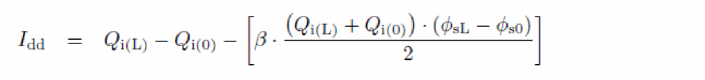
The substrate current is derived as
where
and Xj is the junction depth.
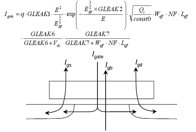
Gate Current
All possible gate leakage currents are schematically shown in Fig. 32.8
Between Gate and Channel, Igate
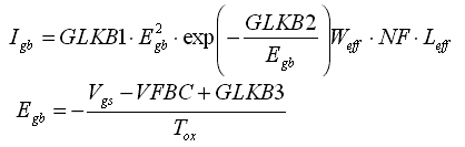
Between Gate and Bulk, Igb
The Igb current under the accumulation condition is modeled as
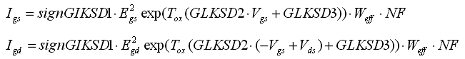
Between Gate and Source/Drain, Igs/Igd
GIDL (Gate-Induced Drain Leakage)
Floating-Body Effect Model
Model selector COFBE as well as COISUB must be set to 1 to activate FBE model. In HiSIM SOI, Qh is modeled as follows:
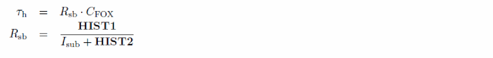
History Effect Model
Time constant for the history effect is modeled as:
where HIST1 and HIST2 are history effect model parameters.
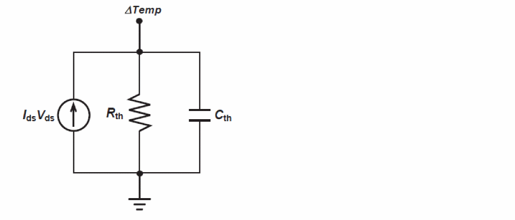
Self-Heating Effect Model
The self-heating effect is modeled as a C-R thermal network with a heat resistance parameter RTH0 and capacitance parameter CTH0. The flag COSELFHEAT must be equal to 1 and RTH0 must not be equal to zero to activate this model. The SHE should be switched on/off only with the model flag COSELFHEAT.
Figure -8
Thermal Network applied for the self-heating effect
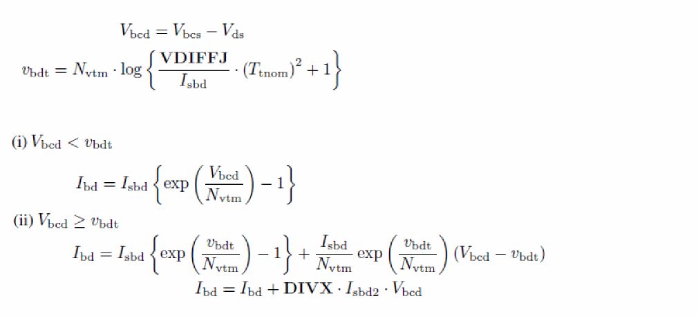
Source/Body and Drain/Body Diode Models
Diode Current
Between drain and body
The forward and backward currents between drain and body are calculated as:
The drain-body current equations are derived as follows:
Between source and body
Body-Tie Models
HiSIM SOI considers both the floating-body and the body-tie structures.
Body-Contact Capacitances
ABTN = LBT ·WBTN
ABTP = LBT ·WBTP
Overlap capacitance of body-tie area
The capacitance between the body-tied gate (hammer head) and the body-tied well is treated as MOS capacitance.
Cgb,bt = CbtN · ABTN + CbtP · ABTP
Overlap capacitance of body-tie periphery
Instance parameters PSBCP and PDBCP are introduced to take into account the overlap capacitance of the periphery of the body-tie contact. These lengths are added to the Weffc as:
Weffc,source = Weffc + PSBCP
Weffc,drain = Weffc + PDBCP
where
Weffc = Wgate - NBT · XWDBT- (2 - NBT) · XWDC
Diode current of body-tie periphery
The diode current also flows at the body-tie periphery. Therefore the lengths determined by the instance parameters PSBCP and PDBCP are added the width as
Weff,source = Weff + PSBCP
Weff,drain = Weff + PDBCP
where
Weff = Wgate - NBT · XWDBT- (2 - NBT) · XWD
Gate-Fringing Capacitance
For body-tied devices, an additional gate-fringing capacitance is considered between gate and body:
Noise Models
1/f Noise Models
The 1/f noise is caused by both the carrier fluctuation and the mobility fluctuation. The final description for the drift-diffusion model is
where the parameters NFALP and NFTRP represent the contribution of the mobility fluctuation and the ratio of trap density to attenuation coefficient, respectively.
Thermal Noise Model
Van der Ziel derived the equation for the spectral density of the thermal drain-noise current at temperature T by integrating the trans-conductance along the channel direction y based on the Nyquist theorem
where  s,
s,  d and
d and  av are mobilities at the source side, the drain side, and averaged, respectively.
Induced Gate Noise Model
Coupling Noise Model
Non-Quasi-Static (NQS) Model
Formation of carrier
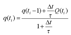
Carriers in the channel take time to build-up as opposed to the Quasi-Static (QS) approximation. To consider this phenomenon in HiSIM, the carrier formation is modeled as
where q(ti) and Q(ti) represent the non-quasi-static and the quasi-static carrier density at time ti, respectively, and  t = ti – ti-1 is valid. Above equation implies that the formation of carriers under the NQS approximation is always delayed in comparison to the QS approximation, which is the basic origin of the NQS effect.
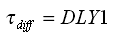
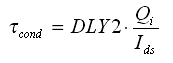
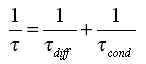
Delay Mechanisms
Weak inversion
Strong inversion
These two delay mechanisms (diffusion and conduction) are combined using the Matthiessen rule:
Applying the same approach for the formation of bulk carriers, leads to the approximation of the bulk carrier delay as an RC delay in the form
Component Statements
Instance Parameters
Refer to the following table for Instance Parameter details:
1
|
l=5.0E-6 m
|
Gate length (Lgate).
|
2
|
w=5.0E-6 m
|
Gate width (Wgate).
|
3
|
ad=0.0 m^2
|
Area of drain junction.
|
4
|
as=0.0 m^2
|
Area of source junction.
|
5
|
pd=0.0 m
|
Perimeter of drain junction.
|
6
|
ps=0.0 m
|
Perimeter of source junction.
|
7
|
ngcon=1.0 -
|
Number of gate contacts.
|
8
|
xgw=0E0 m
|
Distance from gate contact to channel edge.
|
9
|
xgl=0E0 m
|
Offset of gate length.
|
10
|
m=1.0
|
multiplicity factor.
|
11
|
nf=1.0 -
|
Number of gate fingers.
|
12
|
sa=0 m
|
Length of diffusion between gate and STI.
|
13
|
sb=0 m
|
Length of diffusion between gate and STI.
|
14
|
sd=0 m
|
Length of diffusion between gate and gate.
|
15
|
pdbcp=0.0 m
|
Parasitic perimeter length for body contact at drain.
|
16
|
psbcp=0.0 m
|
Parasitic perimeter length for body contact at source.
|
17
|
lod=10.0E-6 m
|
diffusion length between gate and STI edge.
|
18
|
temp=0.0 C
|
Device temperature.
|
19
|
dtemp=0 C
|
Device temperature change.
|
20
|
trise=0 C
|
Device temperature change.
|
21
|
nbt=1.0
|
Number of body contact.
|
22
|
lbt=0.0 m
|
Length of gate over body-contact well.
|
23
|
wbtp=0.0 m
|
Distance of gate protrusion over body-contact well.
|
24
|
wbtn=0.0 m
|
Distance of gate protrusion over body-contact well.
|
25
|
abtn=0.0 m^2
|
Area of N^+ poly area of body contact.
|
26
|
abtp=0.0 m^2
|
Area of P^+ poly area of body contact.
|
27
|
nrs=1.0
|
Number of squares in source .
|
28
|
nrd=1.0
|
Number of squares in drain .
|
29
|
ldrift=1.0E-6 m
|
Parameter for drift region length (drain) .
|
30
|
ldrifts=1.0E-6 m
|
Parameter for drift region length (source) .
|
31
|
rbdb=50.0 Ohm
|
Substrate resistance network.
|
32
|
rbsb=50.0 Ohm
|
Substrate resistance network.
|
Model Definition
model modelName hisimsoi parameter=value ...
Model Parameters
Refer to the following table for Model Parameter details:
1
|
l=5.0E-6 m
|
Gate length (Lgate).
|
2
|
w=5.0E-6 m
|
Gate width (Wgate).
|
3
|
wmax=1.0
|
Maximum width for the model.
|
4
|
wmin=0.0
|
Minimum width for the model.
|
5
|
lmax=1.0
|
Maximum length for the model.
|
6
|
lmin=0.0
|
Minimum length for the model.
|
7
|
copprv=0
|
Previous phi_s flag.
|
8
|
coadov=1
|
Lateral field induced and overlap capacitances are added to intrinsic.
|
9
|
coisub=0
|
Substrate current flag.
|
10
|
cofbe=0
|
Floating-Body Effect flag.
|
11
|
coiigs=0
|
Gate current flag.
|
12
|
cogidl=0
|
GIDL current flag.
|
13
|
coovlp=0
|
Overlap capacitance model selector.
|
14
|
coign=0
|
Induced gate and cross correlation noise flag.
|
15
|
coflick=0
|
1/f noise flag.
|
16
|
cothrml=0
|
Thermal noise flag.
|
17
|
coisti=0
|
STI leakage current flag.
|
18
|
conqs=0
|
Non-quasi-static model flag.
|
19
|
corg=0
|
Gate-contact resistance flag.
|
20
|
coievb=0
|
Valence-band-electron-tunneling-current model flag.
|
21
|
cohist=0
|
History Effect flag.
|
22
|
coselfheat=0
|
Self-Heating flag.
|
23
|
covbsbiz=0
|
Symmetry treatment flag.
|
24
|
colgleff=0
|
Lgate to Leff flag.
|
25
|
coqovsm=1
|
Qover capacitance model selector.
|
26
|
coqbdsm=1
|
Gate/body contact well MOS-capacitance model selector.
|
27
|
cobcnode=0
|
Body contact node flag.
|
28
|
cosubscale=0
|
Switch scaling for Isub.
|
29
|
coisubfb=0
|
Switch Isub in FB mode: 0 with analytical Ids; 1 with iterative Ids.
|
28
|
info=0
|
print information selector.
|
31
|
qhsmax=1e-3
|
Upper limit Qhs .
|
32
|
dvgpsub=0
|
Delta VGPSUB (in addition to VFBSUB).
|
33
|
dvbssub=0
|
Delta VBSSUB for Qh effect.
|
34
|
type=1 -
|
1 for nMOS and -1 for pMOS.
Possible values are p and n.
|
35
|
version=1.40 -
|
Model parameter version accepts only real number values, like 1.30 for version=1.3.0. The available versions are 1.30 and 1.40. Default version is 1.40.
|
36
|
vmax=7.00E+6 cm s^-1
|
Saturation velocity.
|
37
|
bgtmp1=90.25E-6 eV K^-1
|
Temperature dependence of bandgap.
|
38
|
bgtmp2=100.0E-9 eV K-2
|
Temperature dependence of bandgap.
|
39
|
eg0=1.1785 eV
|
Bandgap.
|
40
|
xld=0.0 m
|
Gate overlap length.
|
41
|
xldc=0.0 m
|
XLD for capacitance.
|
42
|
vfbover=0.0 V
|
Flat-band voltage in overlap region.
|
43
|
nover=1E19 cm-3
|
Impurity concentration in overlap region.
|
44
|
xwd=0.0 m
|
Gate overlap width.
|
45
|
xwdc=0.0 m
|
XWD for cap.
|
46
|
saref=1E-6 m
|
Reference distance from STI edge to Gate edge.
|
47
|
sbref=1E-6 m
|
Reference distance from STI edge to Gate edge.
|
48
|
xqy=0.0 m
|
Distance from junction to max field point.
|
49
|
xqy1=0.0 F μm^XQY2-1
|
Vbs-dependence of Qy.
|
50
|
xqy2=2.0 -
|
Lgate-dependence of Qy.
|
51
|
rshg=0.0 Ω/square
|
Gate sheet resistance.
|
52
|
vfbc=(-1.0) V
|
Flat-band voltage.
|
53
|
vbi=1.1 V
|
Built-in potential.
|
54
|
nsubpl=0.001 m^-1
|
Modification of pocket-impurity concentration.
|
55
|
nsubpfac=1 -
|
Modification of pocket-impurity concentration.
|
56
|
parl1=10.0E-9 cm
|
SOI SCE parameter.
|
57
|
parl2=10.0E-9 m
|
Depletion width of channel/contact junction.
|
58
|
lp=0.0 m
|
Pocket penetration length.
|
59
|
nsubp=1.0E+17 cm-3
|
Max pocket concentration.
|
60
|
nsubp0=0.0 -
|
Modification of pocket concentration for narrow W.
|
61
|
nsubwp=1.0 -
|
Modification of pocket concentration for narrow W.
|
62
|
wl1=0.0 m
|
Small-size effect parameter for STI leakage.
|
63
|
wl1p=1.0 -
|
Small-size effect parameter for STI leakage.
|
64
|
wl2=0.0 -
|
Threshold voltage shift due to small-size effect.
|
65
|
wl2p=1.0 -
|
Threshold voltage shift due to small-size effect.
|
66
|
scp1=0.0 -
|
Magnitude of short-channel effect due to pocket.
|
67
|
scp2=0.0 V^-1
|
Vds-dependence of SCE due to pocket.
|
68
|
scp3=0.0 m V^-1
|
Vds-dependence of SCE due to pocket.
|
69
|
sc1=0.0 -
|
magnitude of short-channel effect.
|
70
|
sc2=0.0 V^-1
|
Vds-dependence of short-channel effect.
|
71
|
sc3=0.0 m V^-1
|
Vbs dependence of short-channel effect.
|
72
|
scr1=0.0 -
|
Parameter for SCE via BOX.
|
73
|
scr2=0.0 -
|
Parameter for SCE via BOX.
|
74
|
scr3=0.23 -
|
Parameter for SCE via BOX.
|
75
|
pgd1=0.0 V
|
Strength of poly-depletion effect.
|
76
|
pgd2=1.0 V
|
Threshold voltage of poly-depletion effect.
|
77
|
pgd4=0.0 -
|
Lgate-dependence of poly-depletion effect.
|
78
|
ndep=1.0 -
|
Depletion charge contribution to Eeff.
|
79
|
ninv=0.5 -
|
inversion charge contribution to Eeff.
|
80
|
ninvd=0.0 V^-1
|
inversion charge parameter.
|
81
|
muecb0=300.0 cm2V^-1s^-1
|
Coulomb scattering.
|
82
|
muecb1=30.0 cm2V^-1s^-1
|
Coulomb scattering.
|
83
|
mueph0=300.0E-3 -
|
Phonon scattering.
|
84
|
muephw=0.0 -
|
Phonon-related mobility reduction.
|
85
|
muepwp=1.0 -
|
Phonon-related mobility reduction.
|
86
|
muephl=0.0 -
|
L-dependence of phonon mobility reduction.
|
87
|
mueplp=1.0 -
|
L-dependence of phonon mobility reduction.
|
88
|
muephs=0.0 -
|
Mobility change due to small size.
|
89
|
muepsp=1.0 -
|
Mobility change due to small size.
|
90
|
vtmp=0.0 cm s^-1
|
Temperature-dependence of saturation velocity.
|
91
|
wvth0=0.0 Vμm
|
Threshold voltage shift.
|
92
|
muesr1=2.0E15 cm2V^-1s^-1
|
Surface-roughness scattering.
|
93
|
muesr0=2.0 -
|
Surface-roughness scattering.
|
94
|
muesrl=0.0 −
|
L-dependence of surface roughness on mobility.
|
95
|
muesrw=0.0 −
|
Surface roughness-related mobility change.
|
96
|
mueswp=1.0 -
|
Surface roughness-related mobility change.
|
97
|
mueslp=1.0 -
|
L-dependence of surface roughness on mobility.
|
98
|
muetmp=1.5 −
|
Temperature-dependence of phonon scattering.
|
99
|
bb=2.0 -
|
High-field-mobility degradation.
|
100
|
ddltmax=10.0 -
|
Smoothing coefficient for Vds.
|
101
|
ddltslp=10.0 μm^-1
|
Lgate-dependence of smoothing coefficient.
|
102
|
ddltict=0.0 -
|
Lgate-dependence of smoothing coefficient.
|
103
|
sub1=0.01 V^-1
|
Substrate current coefficient of magnitude.
|
104
|
sub2=20.0 V
|
Substrate current coefficient of exponential term.
|
105
|
sub1l=2.5E-3 m
|
Lgate-dependence of SUB1.
|
106
|
sub1lp=1.0 -
|
Lgate-dependence SUB1.
|
107
|
sub2l=2.0E-6 m
|
Lgate-dependence of SUB2.
|
108
|
svds=3.0 -
|
Substrate current dependence on Vds.
|
109
|
slg=3.0E-8 m
|
Substrate current dependence on Lgate.
|
110
|
svbs=0.5 -
|
Substrate current dependence on Vbs.
|
111
|
svbsl=0.0 -
|
Lgate-dependence of SVBS.
|
112
|
svbslp=1.0 -
|
Lgate-dependence of SVBS.
|
113
|
svgs=0.8 -
|
Substrate current dependence on Vgs.
|
114
|
svgsl=0.0 -
|
Lgate-dependence of SVGS.
|
115
|
svgslp=1.0 -
|
Lgate-dependence of SVGS.
|
116
|
svgsw=0.0 -
|
Wgate-dependence of SVGS.
|
117
|
svgswp=1.0 -
|
Wgate-dependence of SVGS.
|
118
|
slgl=0.0
|
Substrate current dependence on Lgate.
|
119
|
slglp=1.0
|
Substrate current dependence on Lgate .
|
120
|
vfbsub=(-1.0) V
|
Flatband voltage for Isub calculation.
|
121
|
vfbsubl=0.0 −
|
Lgate-dependence of VFBSUB.
|
122
|
vfbsublp=1.0 -
|
Lgate-dependence of VFBSUB.
|
123
|
subdlt=2.0E-3 -
|
Smoothing parameter (hisimsoi_fb only).
|
124
|
hist1=10E-9 V
|
History-effect parameter.
|
125
|
hist2=1E-20 A
|
History-effect parameter.
|
126
|
qhe1=1.5 -
|
FBE parameter.
|
127
|
qhe2=0.35 V
|
FBE parameter.
|
128
|
evb1=0.0 V-2s^-1
|
Electron tunneling from valence band.
|
129
|
evb2=0.0 V m^-1
|
Electron tunneling from valence band.
|
130
|
evb3=0.0 -
|
Electron tunneling from valence band.
|
131
|
fvbs=0.0 -
|
Vbs dependence of Fowler-Nordheim current.
|
132
|
ibpc1=0.0 Ω
|
impact-ionization-induced bulk potential change.
|
133
|
ibpc2=0.0 V^-1
|
impact-ionization-induced bulk potential change.
|
134
|
nsti=5.0E17 cm-3
|
Substrate impurity concentration at STI edge.
|
135
|
wsti=0.0 m
|
Width of high-field region at STI edge.
|
136
|
wstil=0.0 −
|
Channel-length dependence of WSTI.
|
137
|
wstilp=1.0 -
|
Channel-length dependence of WSTI.
|
138
|
wstiw=0.0 −
|
Channel-width dependence of WSTI.
|
139
|
wstiwp=1.0 -
|
Channel-width dependence of WSTI.
|
140
|
scsti1=0.0 -
|
The same effect as SC1 but at STI edge.
|
141
|
scsti2=0.0 V^-1
|
The same effect as SC2 but at STI edge.
|
142
|
vthsti=0.0 V
|
Threshold voltage shift due to STI.
|
143
|
vdsti=0.0 -
|
Vds dependence of STI subthreshold.
|
144
|
muesti1=0.0 m
|
Mobility change due to diffusion length.
|
145
|
muesti2=0.0 -
|
Mobility change due to diffusion length.
|
146
|
muesti3=1.0 -
|
Mobility change due to diffusion length.
|
147
|
nsubpsti1=0.0 m
|
Pocket concentration modifier.
|
148
|
nsubpsti2=0.0 -
|
Pocket concentration modifier.
|
149
|
nsubpsti3=1.0 -
|
Pocket concentration modifier.
|
150
|
nsubcsti1=0.0 m
|
Channel concentration modifier.
|
151
|
nsubcsti2=0.0 -
|
Channel concentration modifier.
|
152
|
nsubcsti3=1.0 -
|
Channel concentration modifier.
|
153
|
tpoly=0.0 m
|
Height of poly-Si gate for fringing cap.
|
154
|
cgbo=0.0 F m^-1
|
Gate-to-B overlap cap.
|
155
|
cgdo=0.0 F m^-1
|
Gate-to-drain overlap cap.
|
156
|
cgso=0.0 F m^-1
|
Gate-to-source overlap cap.
|
157
|
ovslp=2.1E-7 mV^-1
|
Coefficient for overlap capacitance.
|
158
|
ovmag=0.6E0 V
|
Coefficient for overlap capacitance.
|
159
|
js0=1.0E-4 A m-2
|
Saturation current density.
|
160
|
nj=1.0 -
|
Emission coefficient.
|
161
|
xti=2.0 -
|
Temp coefficient for forward current densities.
|
162
|
xti2=0.0 -
|
Temp coefficient for reverse current densities.
|
163
|
vdiffj=1.6E-3 V
|
Diode threshold voltage at junction.
|
164
|
divx=0.0 V^-1
|
Reverse current coefficient.
|
165
|
cj=5.0E-04 F m-2
|
Bottom junc cap/unit area at zero bias.
|
166
|
cjsw=5.0E-10 F m^-1
|
Sidewall junc cap grading coefficient.
|
167
|
cjswg=5.0E-10 F m^-1
|
Sidewall junc cap per unit length at zero bias.
|
168
|
mj=0.33 -
|
Bottom junc cap grading coefficient.
|
169
|
mjsw=0.33 -
|
Sidewall junc cap grading coefficient.
|
170
|
mjswg=0.33 -
|
Gate sidewall junc cap grading coefficient.
|
171
|
pb=1.0 V
|
Bottom junc built-in potential.
|
172
|
pbsw=1.0 V
|
Sidewall junc built-in potential.
|
173
|
pbswg=1.0 V
|
Gate sidewall junc built-in potential.
|
174
|
lover=30E-9 m
|
Overlap length.
|
175
|
clm1=700.0E-3 -
|
Hardness coefficient of channel/contact junction.
|
176
|
clm2=2.0 -
|
Coefficient for QB contribution.
|
177
|
clm3=1.0 -
|
Coefficient for QI contribution.
|
178
|
clm5=1.0 -
|
CLM parameter.
|
179
|
clm6=0.0 −
|
CLM parameter.
|
180
|
vover=10.0E-3 -
|
Velocity overshoot effect parameter.
|
181
|
voverp=100.0E-3 -
|
Leff-dependence of velocity overshoot.
|
181
|
vovers=0.0 -
|
Modification of max velocity due to small size.
|
183
|
voversp=1.0 -
|
Modification of max velocity due to small size.
|
184
|
wfc=0.0 F cm-2 m^-1
|
Threshold voltage change due to cap change.
|
185
|
nsubcw=0.0 −
|
Substrate concentration modifier.
|
186
|
nsubcwp=1.0 -
|
Substrate concentration modifier.
|
187
|
nsubcmax=5E18 cm-3
|
Upper limit of substrate concentration.
|
188
|
nsubcl=0.0 -
|
Lgate-dependence of substrate concentration .
|
189
|
nsubclp=1.0 -
|
Lgate-dependence of substrate concentration .
|
190
|
qme1=0.0 mV
|
Vgs-dependence of quantum mechanical effect.
|
191
|
qme2=0.0 V
|
Vgs-dependence of quantum mechanical effect.
|
192
|
qme3=0.0 m
|
Minimum Tox modification.
|
193
|
gidl1=5.0E-6 A V-3/2C^-1m
|
Magnitude of GIDL.
|
194
|
gidl2=1.0E6 V-2m^-1F-3/2
|
field-dependence of GIDL.
|
195
|
gidl3=300.0E-3 -
|
Vds-dependence of GIDL.
|
196
|
gidl4=0.0 V
|
Threshold for Vds dependence.
|
197
|
gidl5=0.2E0 -
|
High-field correction.
|
198
|
gidlvb=0.5 V3
|
Vb-dependence of GIDL.
|
199
|
gleak1=10.0E3 V-3/2 s^-1
|
Gate-to-channel current coefficient.
|
200
|
gleak2=20.0E6 V^-1/2 m^-1
|
Gate-to-channel current coefficient.
|
201
|
gleak3=300.0E-3 -
|
Gate-to-channel current coefficient.
|
202
|
gleak4=4E0 m^-1
|
Gate-to-channel current coefficient.
|
203
|
gleak5=7.5E3 V m^-1
|
G-t-C short channel correction.
|
204
|
gleak6=250E-3 V
|
G-t-C Vds-dependence correction.
|
205
|
gleak7=1E-6 m2
|
G-t-C L and W dependence correction.
|
206
|
glksd1=1.0E-15 A m V-2
|
G-t-S/D current coefficient.
|
207
|
glksd2=5E6 V^-1 m^-1
|
G-t-S/D current coefficient.
|
208
|
glksd3=(-5E6) m^-1
|
G-t-S/D current coefficient.
|
209
|
glkb1=5E-16 A V-2
|
G-t-S/D current coefficient.
|
210
|
glkb2=1E0 m V^-1
|
G-t-S/D current coefficient.
|
211
|
glkb3=0E0 V
|
G-t-S/D current coefficient.
|
212
|
vzadd0=10.0E-3 V
|
Symmetry conservation coefficient.
|
213
|
pzadd0=5.0E-3 V
|
Symmetry conservation coefficient.
|
214
|
nftrp=10E9 V^-1
|
Ratio of trap density to attenuation coefficient.
|
215
|
nfalp=1.0E-19 cm s
|
Contribution of mobility fluctuation.
|
216
|
cit=0.0 F cm-2
|
Cap caused by the interface trapped carriers.
|
217
|
falph=1.0 sm3
|
Power of f describing deviation of 1/f.
|
218
|
tnom=27.0 C
|
Temperature selected as a nominal value.
|
219
|
dly1=100.0E-12 s
|
Coefficient for delay due to diffusion of carriers.
|
220
|
dly2=0.7E0 -
|
Coefficient for delay due to conduction of carriers.
|
221
|
dly3=0.8E-6 Ω
|
Coefficient for RC delay of bulk carriers.
|
222
|
tfox=3.5E-9 m
|
Front oxide thickness.
|
223
|
tsoi=5.0E-8 m
|
Silicon film thickness.
|
224
|
xj=5.0E-8 m
|
Impurity doping depth.
|
225
|
tbox=1.1E-7 m
|
Buried oxide thickness.
|
226
|
nsubs=3.0E+17 cm-3
|
SOI layer impurity concentration.
|
227
|
nsubb=4.0E+14 cm-3
|
Substrate impurity concentration.
|
228
|
rth0=0.1 Kcm/W
|
Thermal resistance.
|
229
|
cth0=1.0E-7 Ws/(Kcm)
|
Thermal capacitance.
|
230
|
sc4=0.0 -
|
SCE parameter.
|
231
|
ptl=0.0 V^(1-PTP)
|
Punchthrough parameter.
|
232
|
ptp=3.5 -
|
Punchthrough parameter.
|
233
|
pt2=0.0 V^-1
|
Punchthrough parameter.
|
234
|
ptlp=1.0 -
|
Punchthrough parameter.
|
235
|
gdl=0.0 -
|
Strength of high-field effect.
|
236
|
gdlp=0.0 -
|
Modification of channel conductance.
|
237
|
gdld=0.0 m
|
Modification of channel conductance.
|
238
|
pt4=0.0 V^-1
|
Punchthrough parameter.
|
239
|
pt4p=1.0 -
|
Punchthrough parameter.
|
240
|
vgsmin=(-5.0) V
|
Surface potential limiter.
|
241
|
rmin=1E-3 ohm
|
Minimum resistance.
|
242
|
mueph1=25.0E3 cm2V^-1s^-1
|
Phonon scattering.
|
243
|
ldrift=1.0E-6 m
|
Parameter for drift region length (drain) .
|
244
|
ldrifts=1.0E-6 m
|
Parameter for drift region length (source) .
|
245
|
cors=0 -
|
Source side resistance OFF(0)/ON(1).
|
246
|
cord=0 -
|
Drain side resistance OFF(0)/ON(1).
|
247
|
corbulk=0 -
|
Bulk resistance OFF(0)/ON(1).
|
248
|
corbnet=0 -
|
Activate body resistance net (1) or not (0).
|
249
|
rsh=0.0 ohm
|
Drain diffusion sheet resistance .
|
250
|
novers=1E19 cm-3
|
impurity concentration in overlap region.
|
251
|
rdrmued=1.0E3
|
Mobility in drift region (drain).
|
252
|
rdrmues=1.0E3
|
Mobility in drift region (source).
|
253
|
rdrvmaxd=3.0E7
|
Saturation velocity in drift region (drain).
|
254
|
rdrvmax=3.0E7 cm/s
|
Saturation velocity in drift region (drain).
|
255
|
rdrvmaxs=3.0E7
|
Saturation velocity in drift region (source).
|
256
|
rdrmuetmp=0.0 -i
|
Temperature dependence of resistance.
|
257
|
rdrvtmp=0.0 -
|
Temperature dependence of resistance.
|
258
|
rdrdjunc=1.0E-6
|
Junction depth at channel/drift region.
|
259
|
rdrbbd=1
|
Degradation of the mobility in drift region (drain).
|
260
|
rdrbbs=1 -
|
degradation of the mobility in drift region (source).
|
261
|
rdrbbtmp=0 -
|
Temperature coefficient of RDRBB.
|
262
|
rdrvmaxw=0.0 -
|
Wgate dependence of the saturation velocity in drift region.
|
263
|
rdrvmaxwp=1.0 -
|
Wgate dependence of the saturation velocity in drift region.
|
264
|
rdrvmaxl=0.0 -
|
Lgate dependence of the saturation velocity in drift region.
|
265
|
rdrvmaxlp=1.0 -
|
Lgate dependence of the saturation velocity in drift region.
|
266
|
rdrmuel=0.0 -
|
Lgate dependence of the mobility in drift region.
|
267
|
rdrmuelp=1.0 -i
|
Lgate dependence of the mobility in drift region.
|
268
|
rbdb=50.0 Ω
|
Substrate resistance network.
|
269
|
rbsb=50.0 Ω
|
Substrate resistance network.
|
270
|
copt=0 -
|
flag punchthrough.
|
271
|
copspt=0 -
|
flag Ps0 method for deep punchthrough.
|
272
|
xjpt=5.0E-8 m
|
Junction depth for deep punchthrough.
|
273
|
njunc=1e20 cm-3
|
Junction doping conc; deep punchthrough.
|
274
|
mupt=0.0 m2/V/s
|
Mobility for deep punchthrough.
|
275
|
vfbpt=0.0 V
|
dVfb for deep punchthrough.
|
276
|
pslimpt=0.0 V
|
Ps0 limit for deep punchthrough.
|
277
|
rbulk0=0.0 Ω
|
Offset of bulk resistance.
|
278
|
rbulkw=0.0 Ω/m
|
Bulk resistance per width.
|
279
|
vfbbtp=0.12 V
|
Flatband voltage for overlapped MOSFET part.
|
280
|
cbtbn=0.0 F/m2
|
N^+ poly capacitance.
|
281
|
cbtbp=0.0 F/m2
|
P^+ poly capacitance.
|
282
|
xwdbt=0.0 m
|
BT overlap width.
|
Output Parameters
Refer to the following table for Output Parameter details:
|
1
|
meff
|
Effective multiplicity factor (m-factor).
|
Operating-Point Parameters
Refer to the following table for Operating-Point Parameter details:
1
|
rdd (Ω)
|
Drift Resistance on Drain side.
|
2
|
rsd (Ω)
|
Drift Resistance on Source side.
|
3
|
rbulk (Ω)
|
Body Contact Resistance.
|
4
|
idse (A)
|
Drain-Source current.
|
5
|
isuba (A)
|
Substrate current.
|
6
|
igidle (A)
|
Gate-Induced Drain Leakage current.
|
7
|
igisle (A)
|
Gate-Induced Source Leakage current.
|
8
|
igde (A)
|
Gate-Drain current.
|
9
|
igse (A)
|
Gate-Source current.
|
10
|
igbe (A)
|
Gate-Substrate current.
|
11
|
ggm (S)
|
Transconductance.
|
12
|
ggds (S)
|
Channel conductance.
|
13
|
ggmbs (S)
|
Body effect (Back gate) transconductance.
|
14
|
ggmt (S)
|
Temperature transconductance.
|
15
|
deltemp (S)
|
Temperature.
|
16
|
vone (V)
|
Threshold voltage.
|
17
|
vdsate (V)
|
Saturation voltage.
|
18
|
qge (C)
|
Gate charge.
|
19
|
qde (C)
|
Drain charge.
|
20
|
qse (C)
|
Bulk charge.
|
21
|
cggbd (F)
|
g-g MOSFET capacitance.
|
22
|
cgdbd (F)
|
g-d MOSFET capacitance.
|
23
|
cgsbd (F)
|
g-s MOSFET capacitance.
|
24
|
cbgbd (F)
|
b-g MOSFET capacitance.
|
25
|
cbsbd (F)
|
b-s MOSFET capacitance.
|
26
|
cbdbd (F)
|
b-d MOSFET capacitance.
|
27
|
cdgbd (F)
|
d-g MOSFET capacitance.
|
28
|
cddbd (F)
|
d-d MOSFET capacitance.
|
29
|
cdsbd (F)
|
d-s MOSFET capacitance.
|
30
|
ibdb (A)
|
b-d Diode current.
|
31
|
ibsb (A)
|
b-s Diode current.
|
32
|
gbd (S)
|
b-d Diode conductance.
|
33
|
gbs (S)
|
b-s Diode conductance.
|
34
|
capbdb (F)
|
b-d Diode capacitance.
|
35
|
capbsb (F)
|
b-s Diode capacitance.
|
Return to top