Model Equations
All the equations of the model are detailed in this section. The complete calculations of the surface potentials are given in Appendix A and Appendix B, and some useful functions are described in Appendix C.
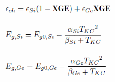
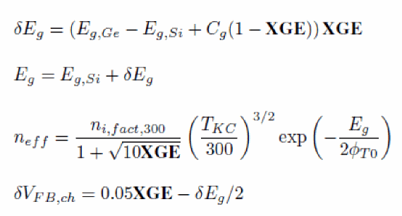
Internal parameters including temperature dependences
The calculations include temperature dependences and are carried out from local scale parameters. Local scale parameters are in capital characters and bold font.
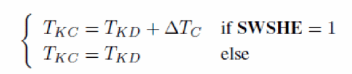
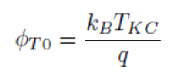
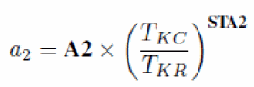
Transistor temperature
The current is evaluated using the following procedure. The master equation for drift current is given by:
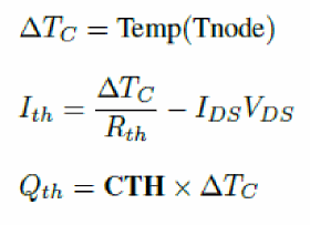
As in Leti-UTSOI1, a temperature node is used to compute the elevation of the channel temperature with respect to the circuit temperature due to self-heating when the SWSHE flag is set to 1. This temperature elevation is given by ![]() . The channel temperature
. The channel temperature ![]() is thus given by:
is thus given by:
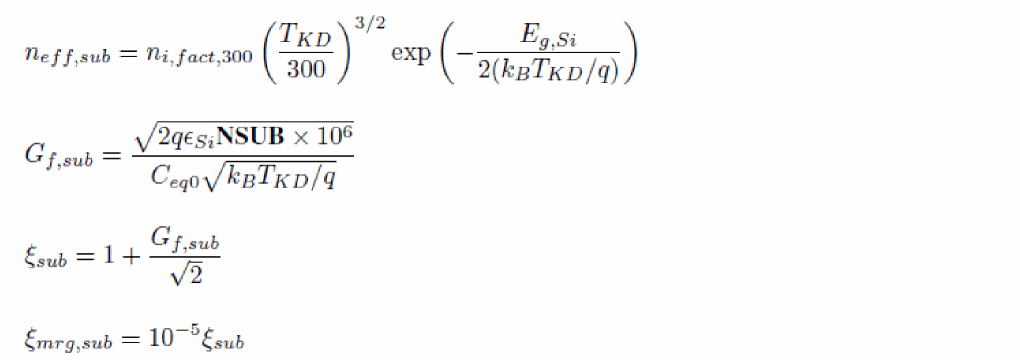
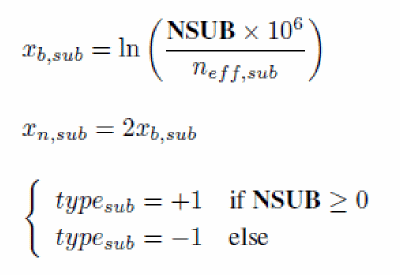
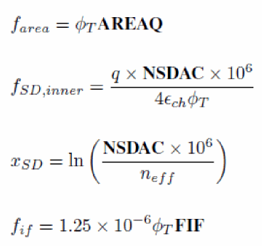
Local process parameters
Interface coupling internal parameters
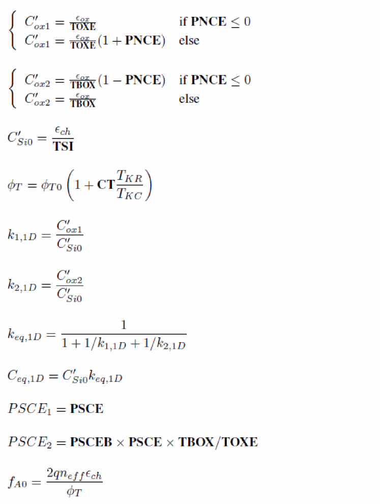
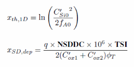
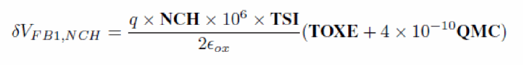
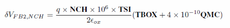
Drain Induced Barrier Lowering internal parameters
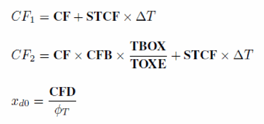
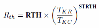
Backplane internal parameters
Since the backplane is located under the buried oxide of the device, it is assumed that its temperature is that of the environment. Thus, the self-heating effect is not included for the corresponding parameters and temperature ![]() is considered.
is considered.
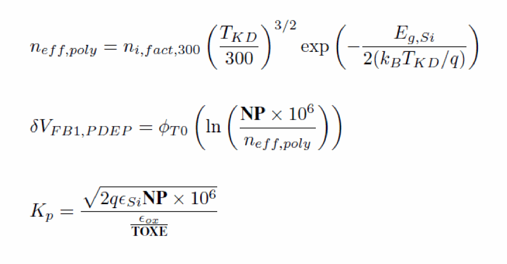
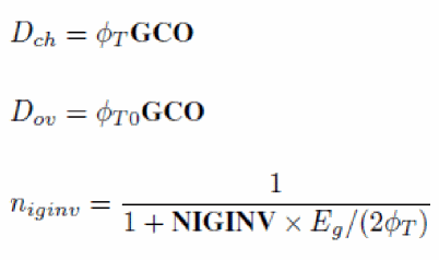
Gate poly-depletion parameters
When SWPDEP = 1, Gate poly-depletion is activated.
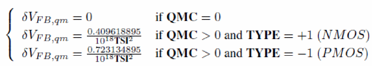
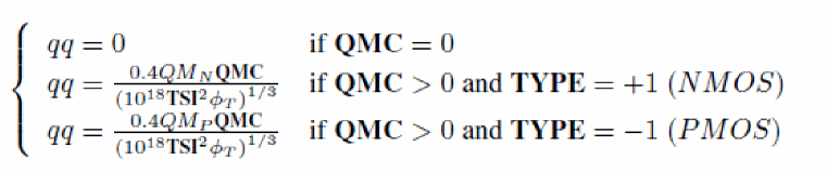
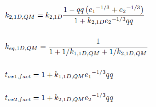
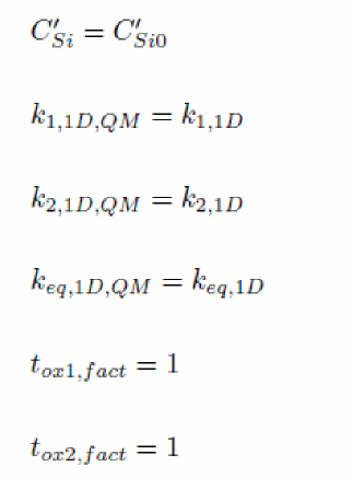
Quantum mechanical correction internal parameters
Mobility internal parameters
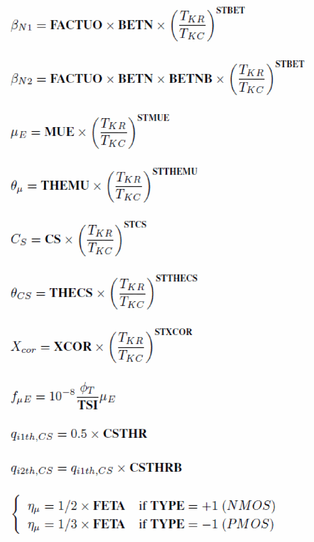
Series resistance internal parameters
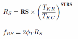
Velocity saturation internal parameters
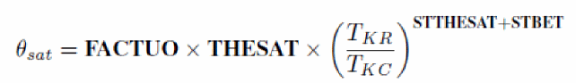
Notice the presence of the FACTUO pre-factor and of STBET in the temperature exponent. This contributes to decouple velocity saturation parameters from low longitudinal field mobility ones, and makes in particular STTHESAT the temperature exponent of the saturation velocity itself.
Channel Length Modulation internal parameters
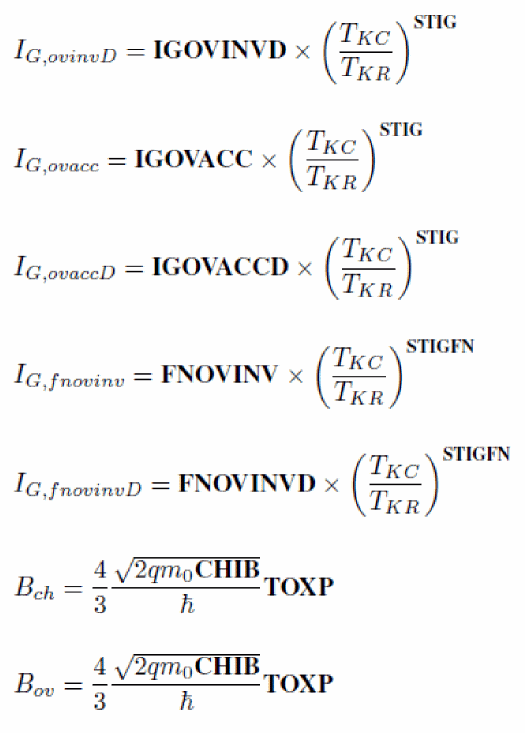
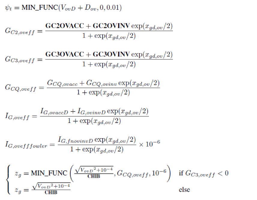
Gate current internal parameters
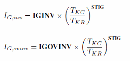
Note that, Bch and Bov are equal in L-UTSOI, since the Leti-UTSOI1 parameter TOXOV has been removed.
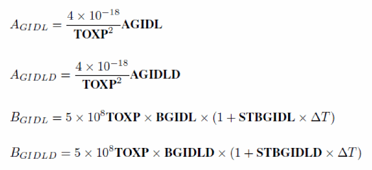
Gate Induced Drain/Source Leakage (GIDL/GISL) internal parameters
Impact ionization internal parameters
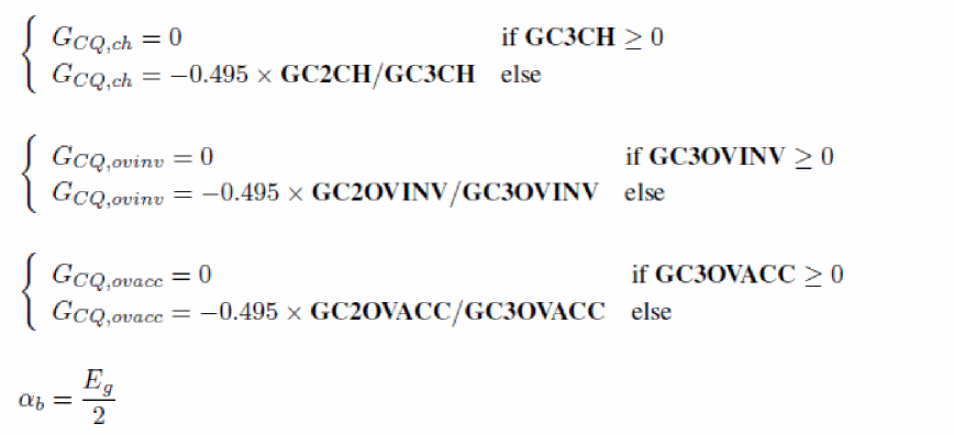
Charge model internal parameters
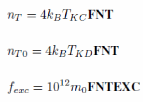
Self-heating internal parameters
Noise model internal parameters
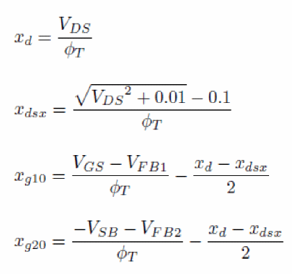
Terminal voltage conditioning
The input voltages used in the model are VGS, VDS and VSB in nMOSFET and positive VDS configuration (that is, sign of external voltages is reversed for pMOSFET, and source/drain are interchanged in case of negative VDS), from which VSD, VGD, VDB and VGB are computed. Then, dimensionless quantities are defined from these voltages.
Voltages for channel current and intrinsic charge models
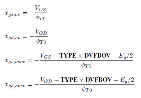
Voltages for overlap currents and charges
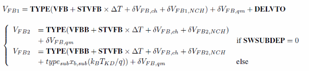
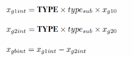
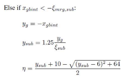
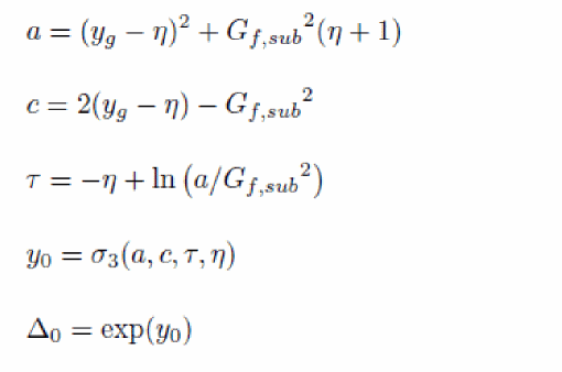
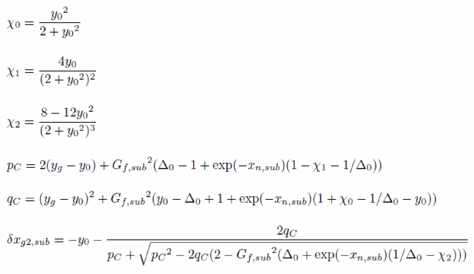
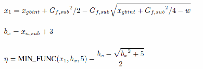
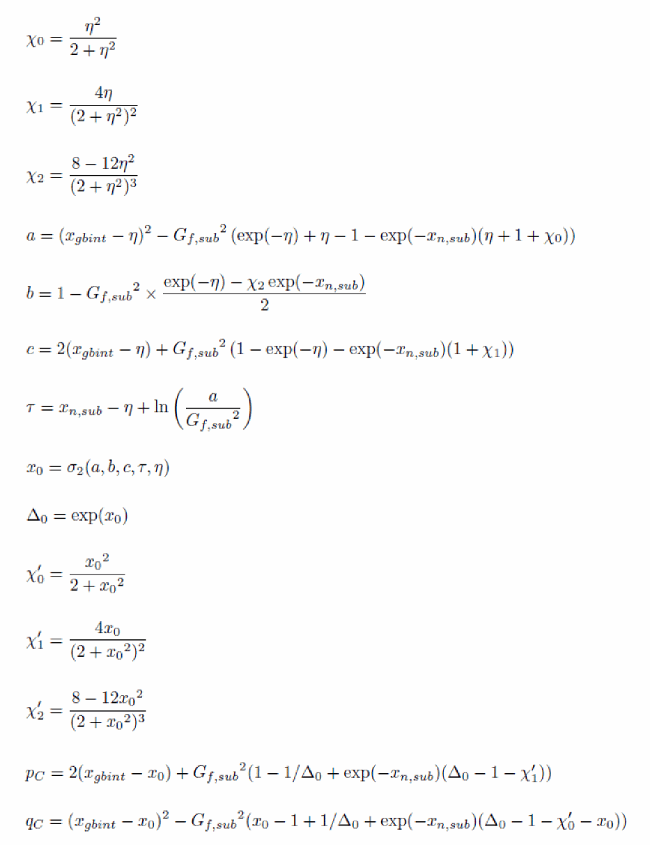
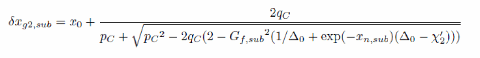
Backplane depletion
Depletion of the backplane is accounted for through the calculation of an effective backplane bias ![]() . If backplane depletion is not activated (SWSUBDEP=0), then
. If backplane depletion is not activated (SWSUBDEP=0), then ![]() is simply given by:
is simply given by:
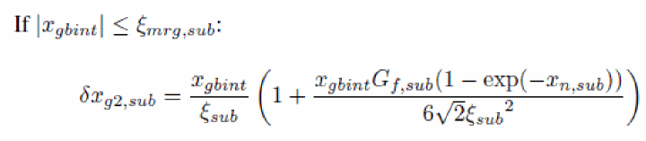
On the contrary, if backplane depletion is activated (SWSUBDEP=1), then the computation of ![]() uses a PSP-like surface potential calculation sequence. This computation is based on the analogy that the backplane is considered as the channel of a bulk MOSFET, which gate electrode is the front gate and which gate oxide capacitance is equal to the front gate oxide capacitance in series with the channel film capacitance and the buried oxide capacitance. The detailed calculation of
uses a PSP-like surface potential calculation sequence. This computation is based on the analogy that the backplane is considered as the channel of a bulk MOSFET, which gate electrode is the front gate and which gate oxide capacitance is equal to the front gate oxide capacitance in series with the channel film capacitance and the buried oxide capacitance. The detailed calculation of ![]() is:
is:
Channel current
This part is dedicated to the calculation of the MOSFET channel current. Since this calculation preserves the formal symmetry between front and back interfaces, it is valid not only for Ultra-Thin Body and Buried oxide FDSOI transistors, but also for Independent Double Gate MOSFETs.
Quantum mechanical correction in subthreshold regime
To account for quantum confinement when the effect is activated (QMC>0), the effective geometry of the device is modified. In the correction detailed here, it is assumed that there is no charge in the channel. Note that his correction is only valid in the subthreshold regime.
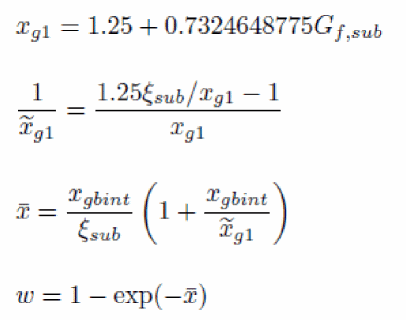
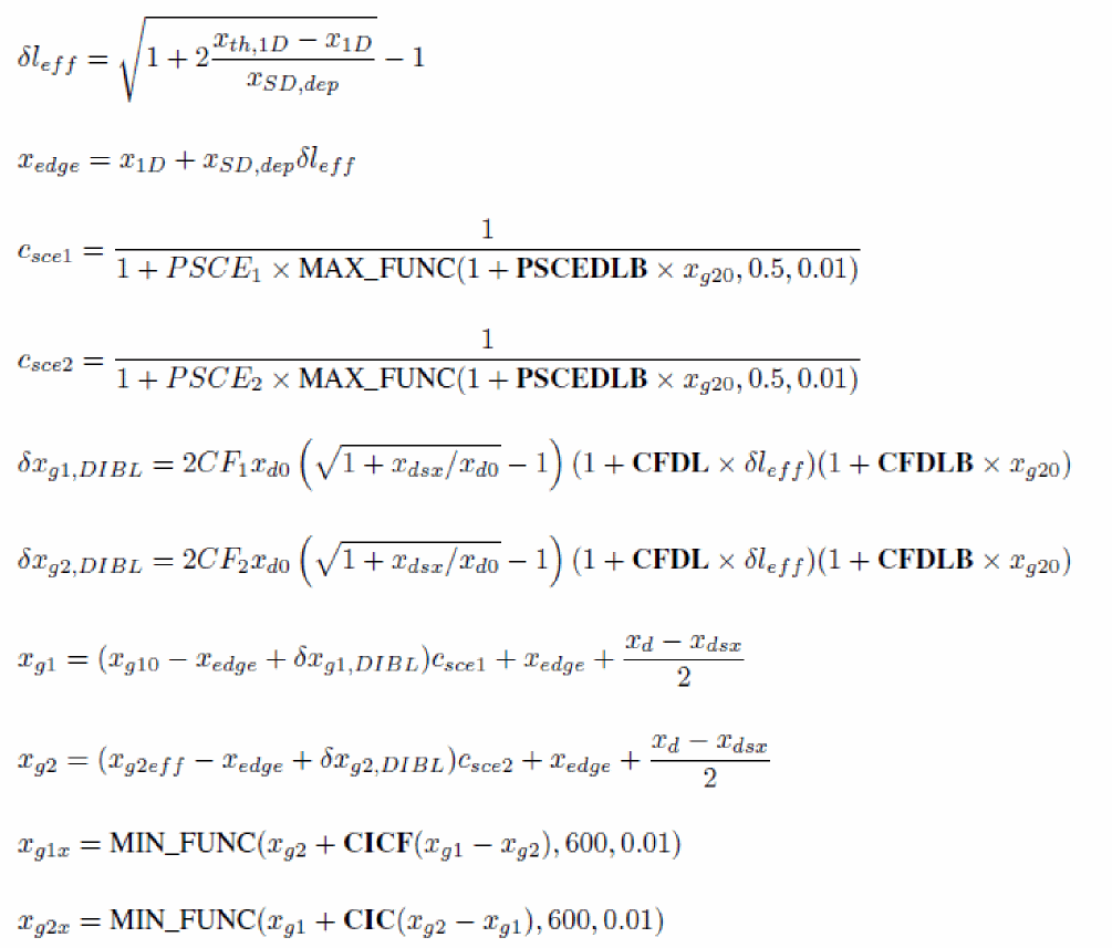
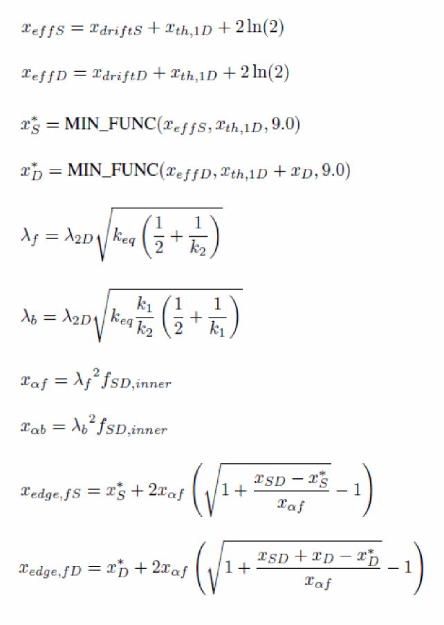
Short channel effects
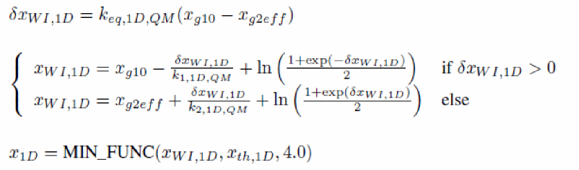
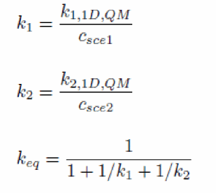
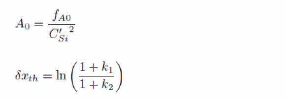
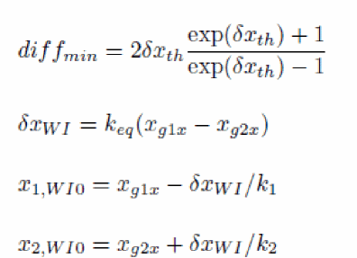
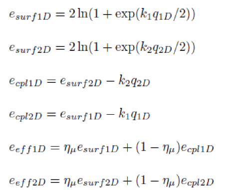
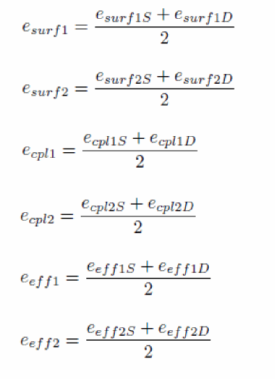
Interface coupling in subthreshold regime
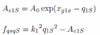
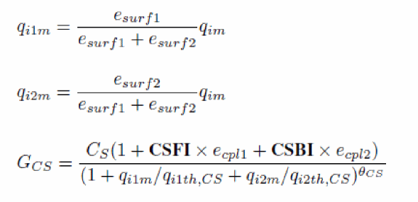
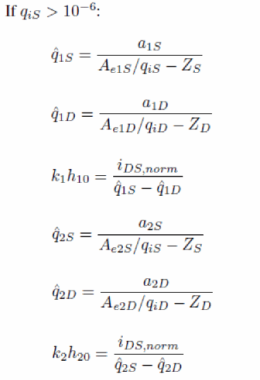
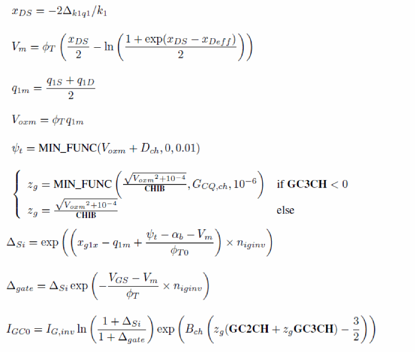
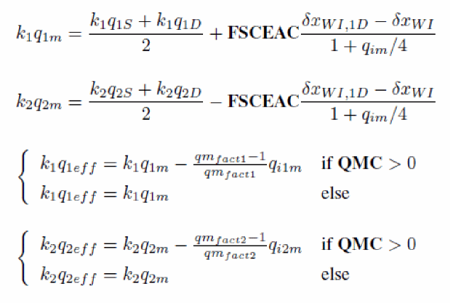
Inversion charge and related quantities at source side
The gate charge density at the source side q1S, normalized to ![]() , is computed as:
, is computed as:
Then, inversion and back gate charge densities, normalized to ![]() and
and ![]() respectively, are calculated:
respectively, are calculated:
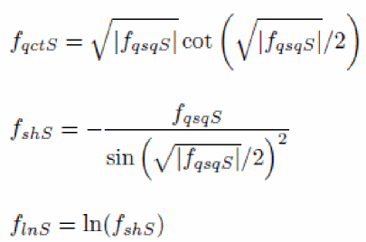
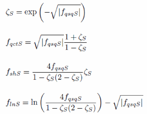
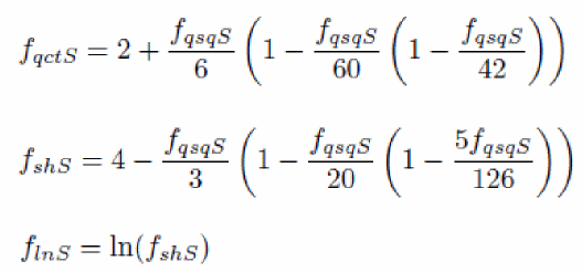
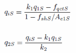
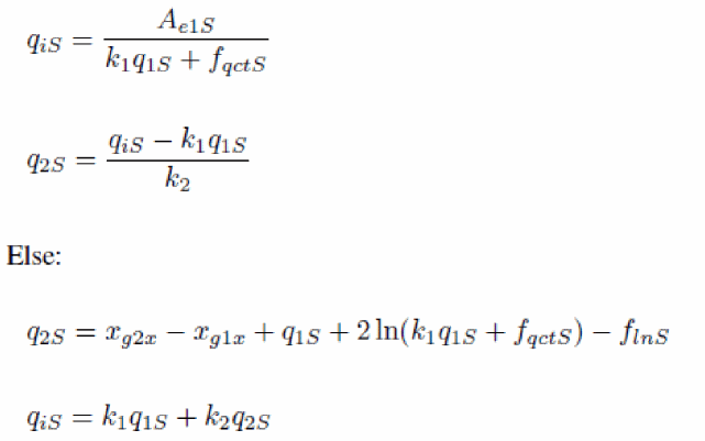
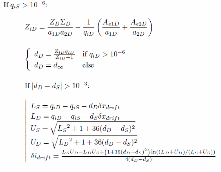
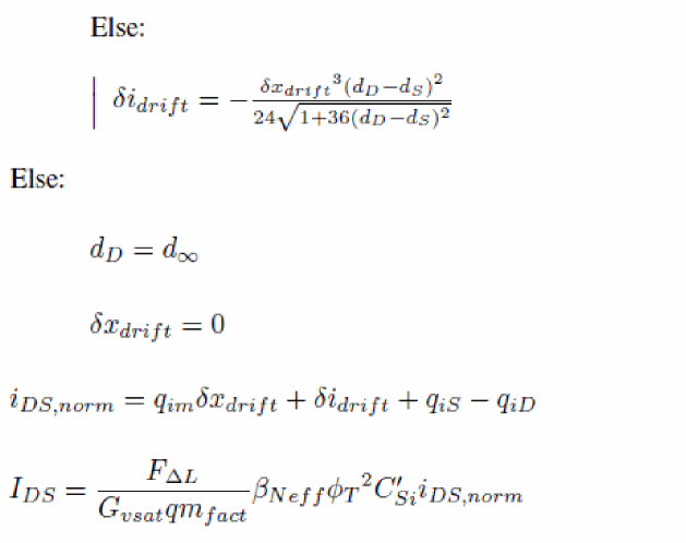
Some required quantities, including the drift electrostatic potential, are computed:
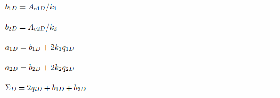
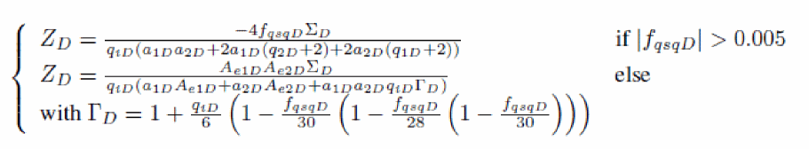
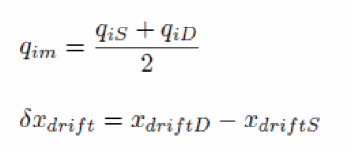
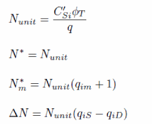
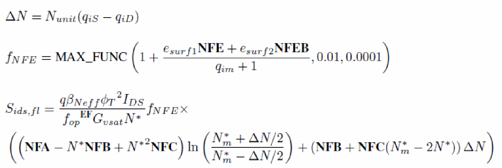
Mid-point inversion charge
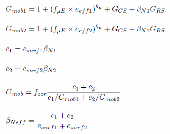
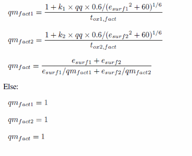
Mobility attenuation and series resistance
Front and back transverse effective fields, normalized to ![]() :
:
Mid-values of surface and effective fields:
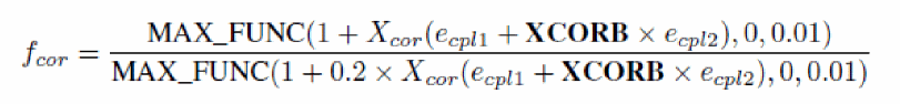
Non-universality correction factor:
Total mobility degradation term, including high field mobility effect:
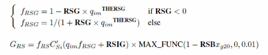
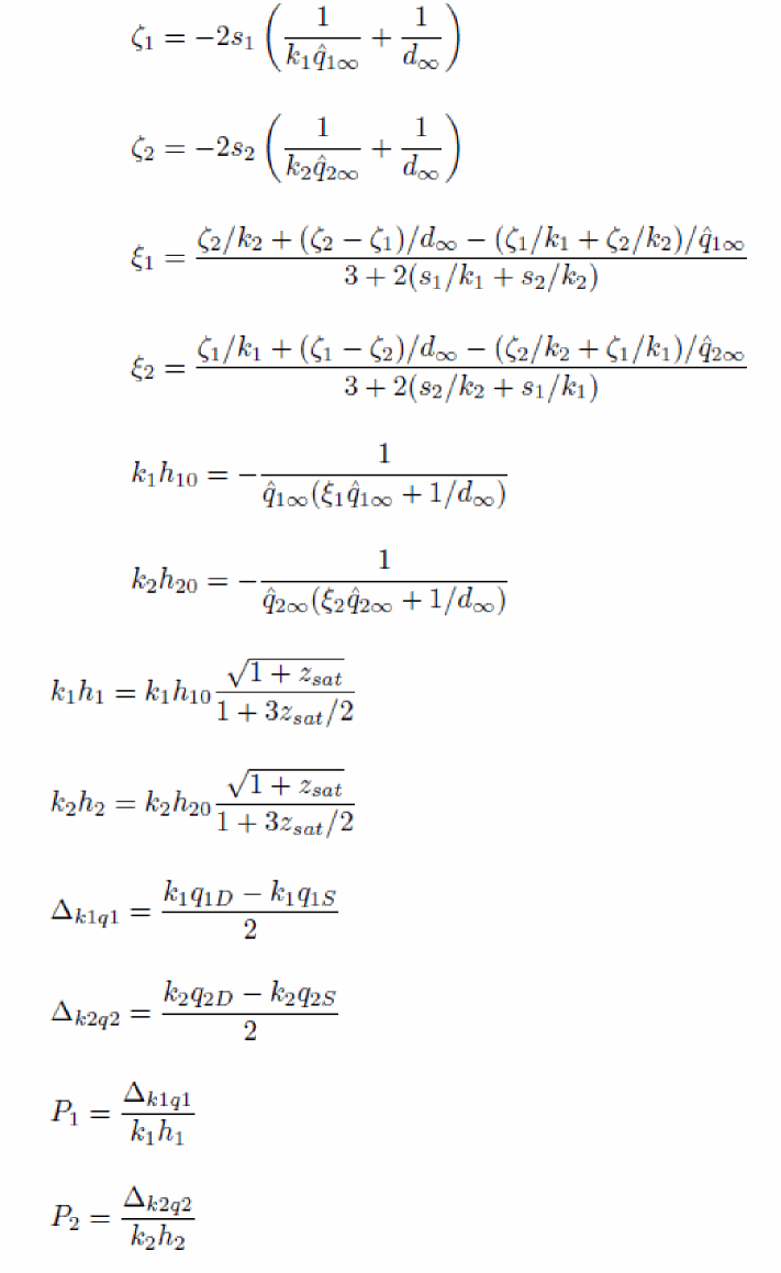
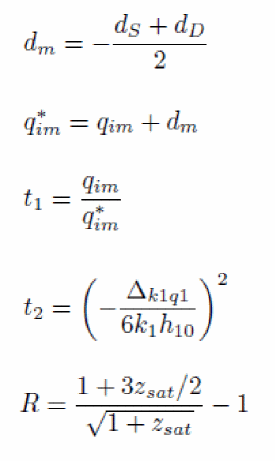
Channel length modulation
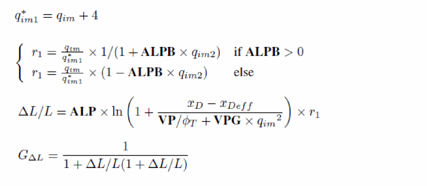
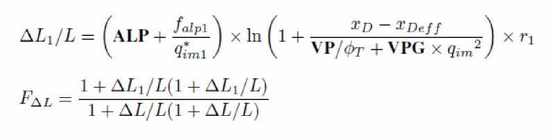
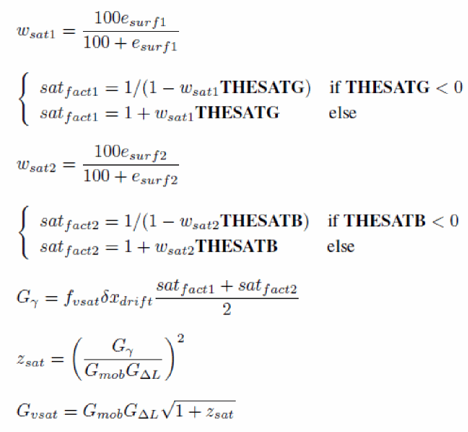
Velocity saturation
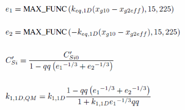
Quantum confinement
Here is detailed the second quantum confinement correction that complements the correction described in Quantum mechanical correction internal parameters.
Channel current
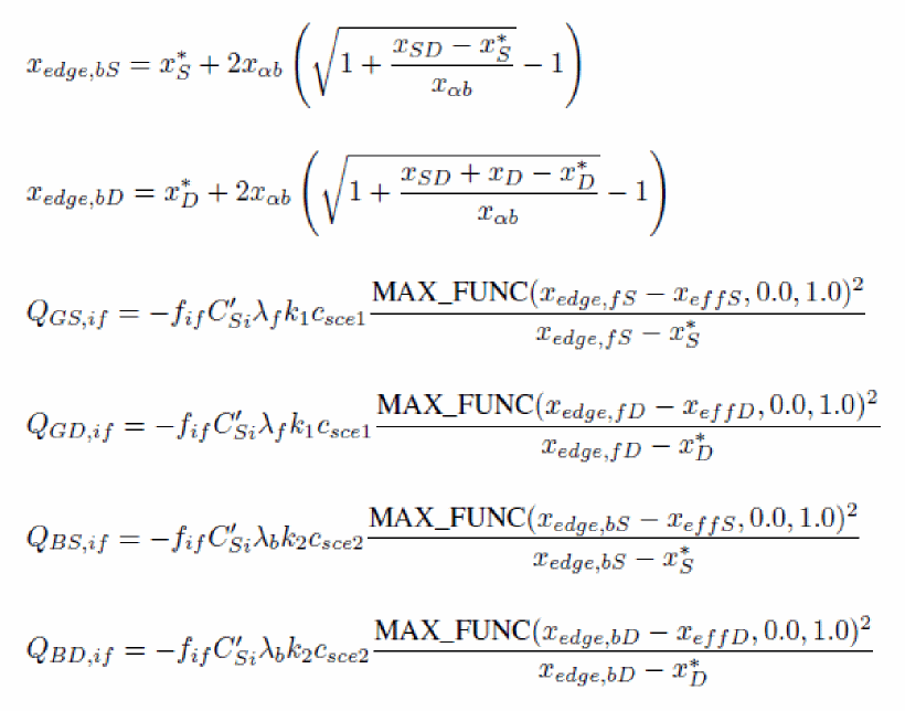
Gate current, intrinsic charges and overlap related variables
Effective gate charge at front and back interfaces
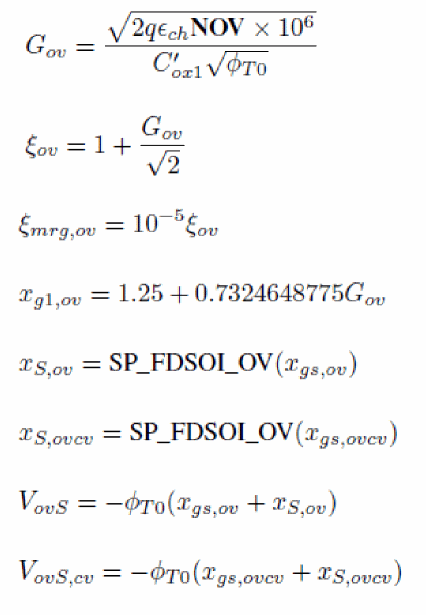
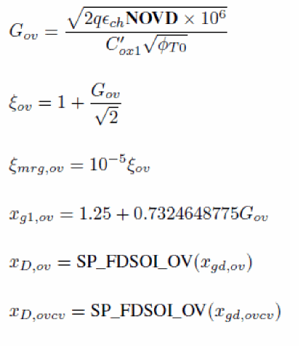
Surface potential and gate dielectric voltage drop in gate-source overlap region
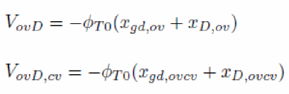
Surface potential and gate dielectric voltage drop in gate-drain overlap region
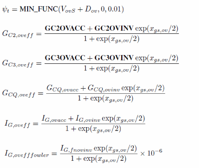
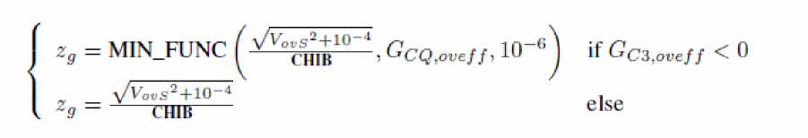
Gate current
The gate current calculation is not carried out when the flag SWIGATE is set to 0.
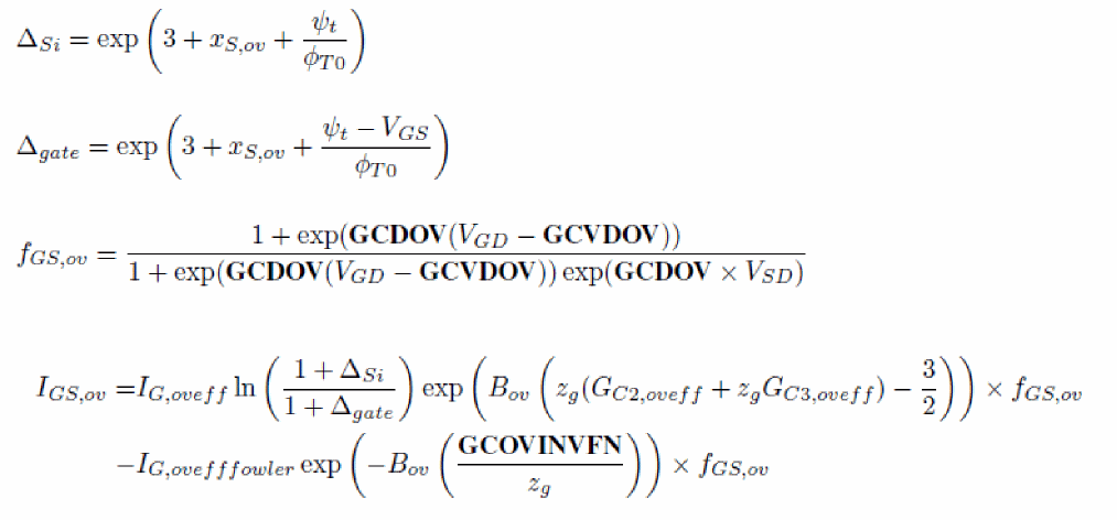
Gate to source overlap component
Gate to drain overlap component
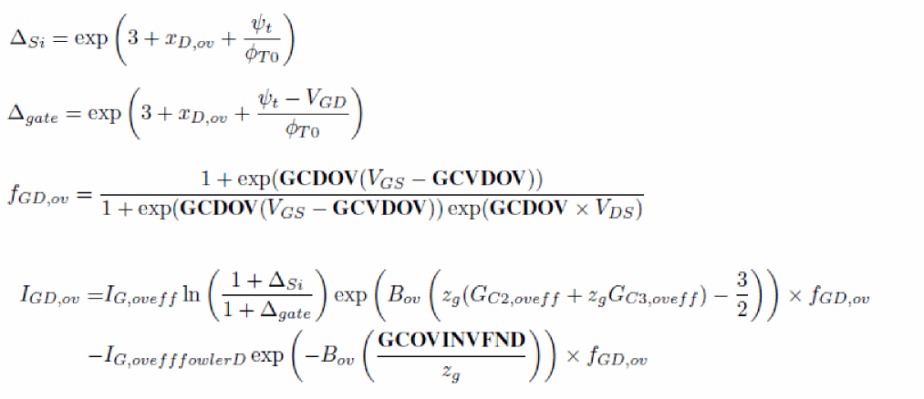
Gate to channel component
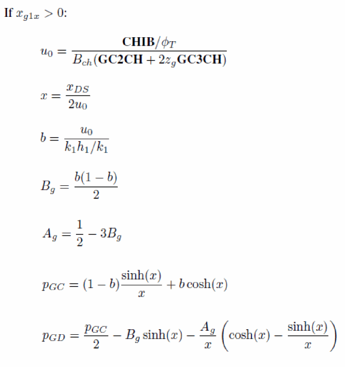
Source/drain partitioning of gate to channel current
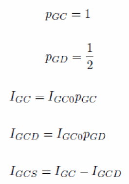
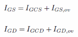
Gate to source and gate to drain total currents
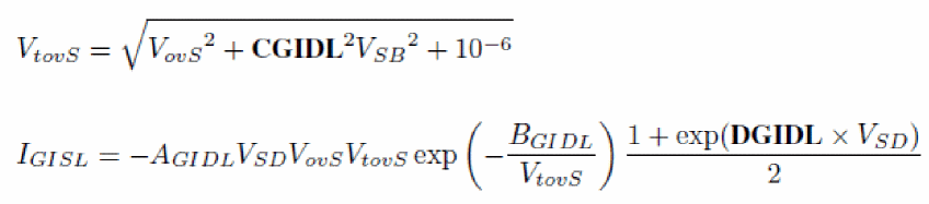
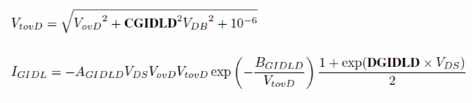
Gate Induced Drain/Source Leakage (GIDL/GISL)
Gate induced source leakage
Gate induced drain leakage
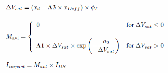
Impact ionization current
The following equations are only calculated when SWIMPACT = 1.
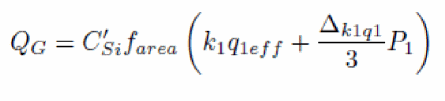
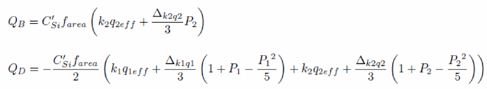
Charge model
Quantum mechanical corrections
Intrinsic charge model
Parasitic charges
Inner fringe charges are computed if FIF > 0.
Outer fringe and overlap charges:
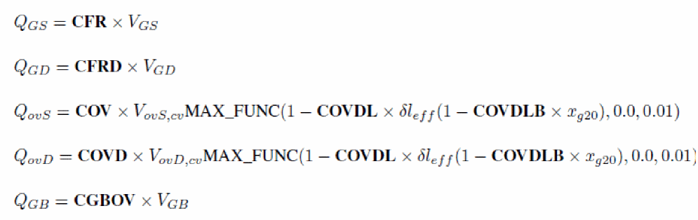
Drain to source direct coupling:
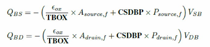
Substrate extrinsic charge model:
Self-heating
A temperature node named Tnode is used to compute the channel temperature elevation induced by the self-heating effect.
Noise model
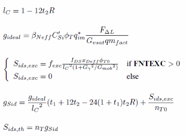
Channel thermal noise
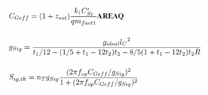
Induced gate noise
Induced gate noise and its correlation with drain thermal noise are computed only when the SWIGN flag is set to 1.
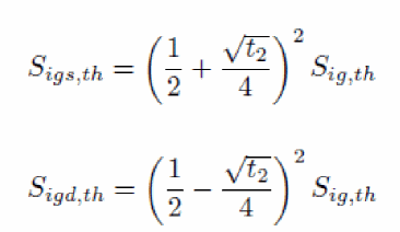
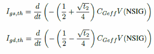
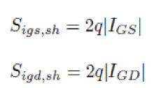
The gate induced noise current is finally partitioned between the gate-source and the gate-drain branches, with a VDS dependent fraction equal to ![]() and
and ![]() respectively. The noise currents in these two branches are thus perfectly correlated and correspond to the following spectral densities:
respectively. The noise currents in these two branches are thus perfectly correlated and correspond to the following spectral densities:
Drain and gate thermal noise correlation
VerilogA implementation of induced gate noise and correlation
As there is no noise function with frequency dependence suitable for the induced gate noise in VerilogA, an internal node NSIG linked to the ground through a parallel RC circuit is used.
Consider the following circuit:
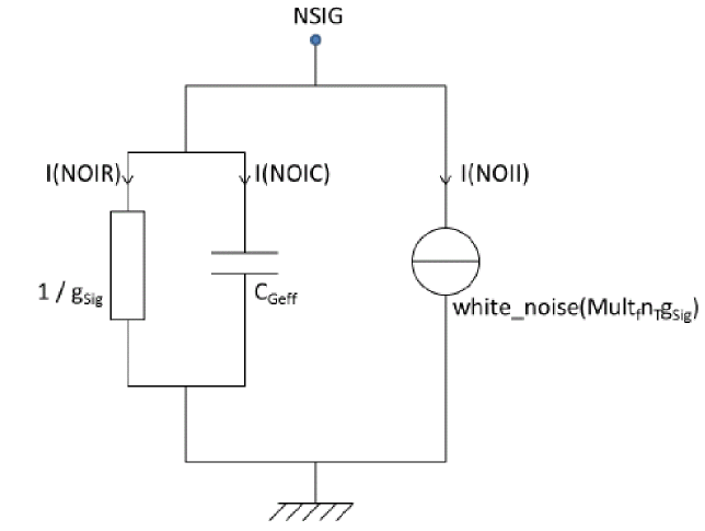
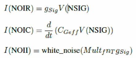
The equivalent circuit is described in the figure shown above and the currents in the different branches are given by:
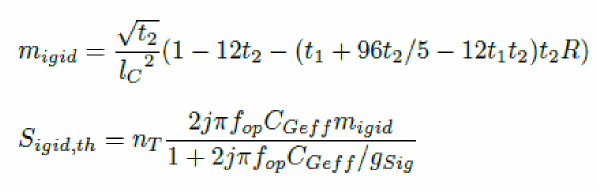
The noise current in the gate-source and gate-drain branches is obtained by:
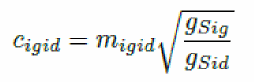
A variable cigid is then defined to obtain the correct correlation between the drain thermal noise current and the gate induced one:
The channel thermal noise current is finally given as the sum of an uncorrelated part and a correlated one:
Channel flicker noise
Shot noises
Impact ionization current shot noise
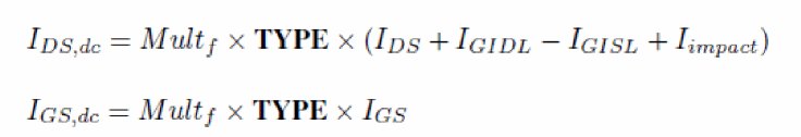
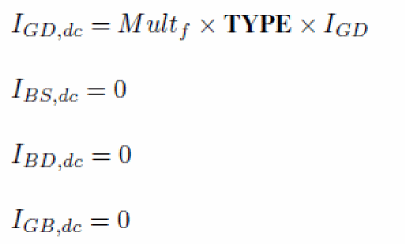
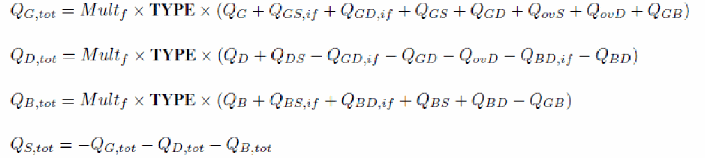
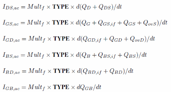
Total currents and charges
Static currents
Total charges
Dynamic currents
Return to top