HiCUM Model Version 2.2
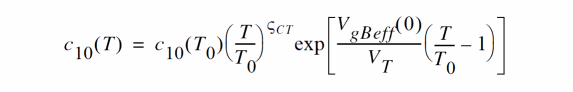
Temperature Dependent Bandgap Voltage
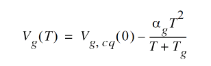
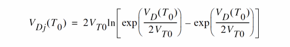
For compact model and application purposes, it is sometimes more convenient to re-write the above equation in terms of a reference temperature T0 (e.g. for parameter extraction), which gives
and the bandgap voltage at the measurement reference temperature,
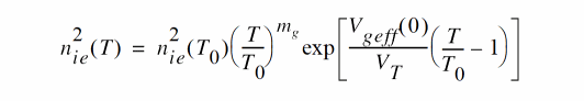
The choice of the bandgap description also influences the formulation of the effective intrinsic carrier density, which now reads
Transfer current
Base Region Reach-Through
Temperature Dependence
Prefactor
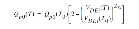
Zero-Bias Hole Charge
Base Currents
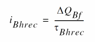
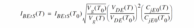
Excess Base Current from Recombination at the BC Barrier
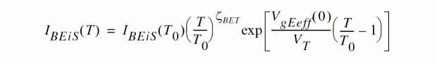
Temperature Dependent Junction Current Components

Depletion Capacitances and Charges
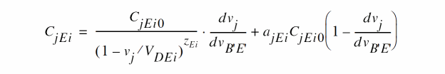
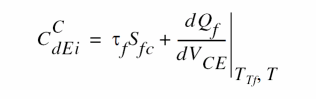
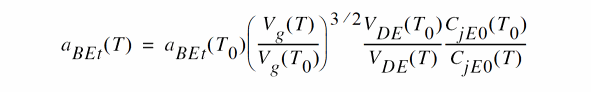
Bias Dependence of Base-Emitter Component
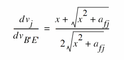
External Depletion Capacitances
The formulation for the depletion capacitances CjEp also has been changed from exponential to hyperbolic smoothing functions.
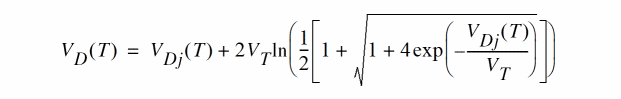
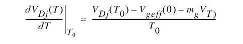
Temperature Dependence of Built-in Voltages
For the bandgap voltage formulation, the above equation reads
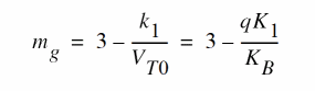
which reduces to the classical equation (that assumes a linear temperature dependence of Vgeff) if mg = 3. Finally, the new built-in voltage is calculated as

Minority Charge
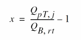
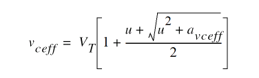
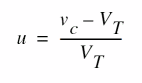
Effective Collector Voltage and Critical Current
Diffusion Capacitances
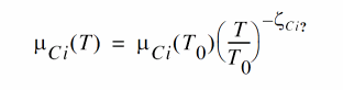
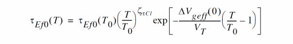
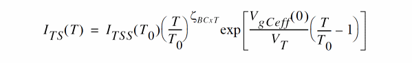
Temperature Dependence
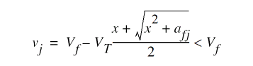
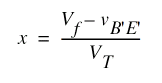
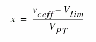
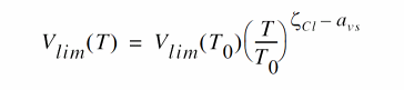
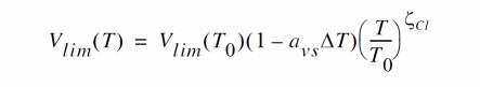
Critical Voltage Vlim
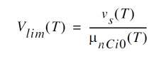
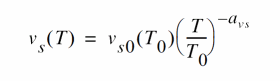
Inserting the temperature dependence of the collector electron mobility into the Vlim(T) equation gives the physics-based formulation
The following equation replaces the formulation used in version 2.1:
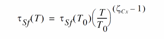
Emitter Transit Time
Collector Current Spreading
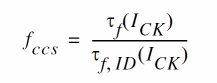
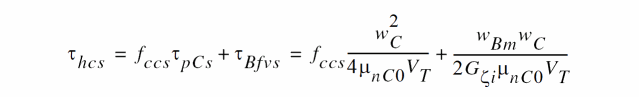
The original model parameter τhcs is be extracted from measurements together with the partitioning factor
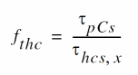
Thus, during preprocessing for model card generation, the modified extracted time constant
is calculated and used as a model parameter.
Internal Base Resistance
In Version 2.1, the impact of the minority charge at the emitter periphery during large-signal switching on the lumped internal base resistance was taken into account by the equation
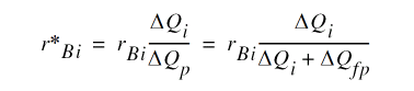
For the case of a large negative BC voltage and a low forward BE voltage
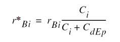
can become zero, causing a division by zero and a pole in the bias dependent rBi characteristic. Although this case is rare and is mostly likely caused by bad (non-physical) parameter combinations, it needs to be avoided under any circumstances. Therefore, to ensure numerical stability QjCi is dropped, leading to the modified formulation of the charge difference
In the corresponding small-signal equation,
the internal capacitance has also to be modified to
Another change of the formulation for the internal base resistance is that the parameter KRBI is dropped. It was introduced about 10 years ago and intended to be used for changing during h.f. noise analysis due to the many uncertainties in bipolar transistor noise mechanisms and theory. With a better understanding of noise in bipolar transistors and many experimental investigations performed recently for advanced processes, this empirical parameter does not seem to be required anymore.
Base-emitter Tunnelling Component
Location of the Current Source
Temperature Dependence
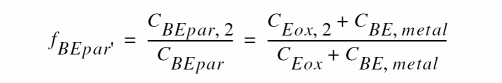
Parasitic Base-Emitter Capacitance Partitioning
Substrate Transistor
Related Topics
Spectre HICUM Model Compared to Public HICUM Model
Return to top