Wafer-Level Packaging
During manufacturing, dies are generally created in batches where many dies are created on one wafer board. When the dies are laid out on the wafer, a space is left between each die boundary so that the scriber can cut the individual dies. This space (scribe area) is wide enough for the saw blade to pass through without affecting the components on the die. When a saw cuts, it removes a channel on the material it is cutting. The figure below shows the scribe area between dies on a wafer board.
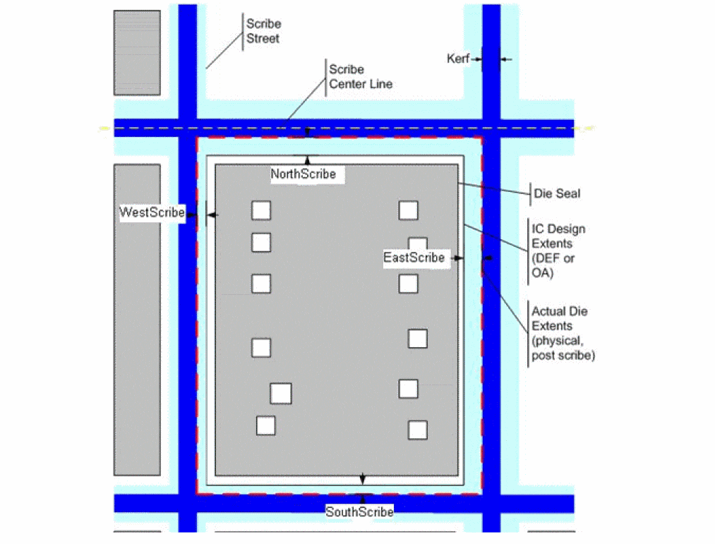
Previously, when you created an Edit-in-Concert die in an IC tool (or imported the die), its physical extents were based on the design extents from the IC design tool, not the actual physical qualities of the die. Yet, you need to consider these actual physical extents when placing dies in a component substrate layout. You must use them for any measurement, clearance, assembly, or placement rule checks that you perform in the component substrate design. This is particularly important in situations, such as measuring the clearance between the 3D path of a bond wire and the edge of the die, or the distance between closely-spaced components. If you do not use the actual die size (including the scribe area), you may place components too closely together in the layout design and, at the time of manufacturing, that will conflict with the placement of other components.
Related Topics
Stackup Information in Substrate
Return to top