Stackup Information in Substrate
The stackup information defines all the layers in the substrate that will be manufactured. This includes conductive layers, dielectric layers, paste layers, bond wires, pads, and shield planes.
The information necessary to complete an accurate stackup includes material, layer type, name, thickness, dielectric constant, and electrical conductivity.
The stackup of a component is important, not only for the physical characteristics, but also for electrical and thermal characteristics. With proper stackup construction, electrical and thermal simulations can provide a more accurate analysis of behavior. Without it, results become skeptical at best.
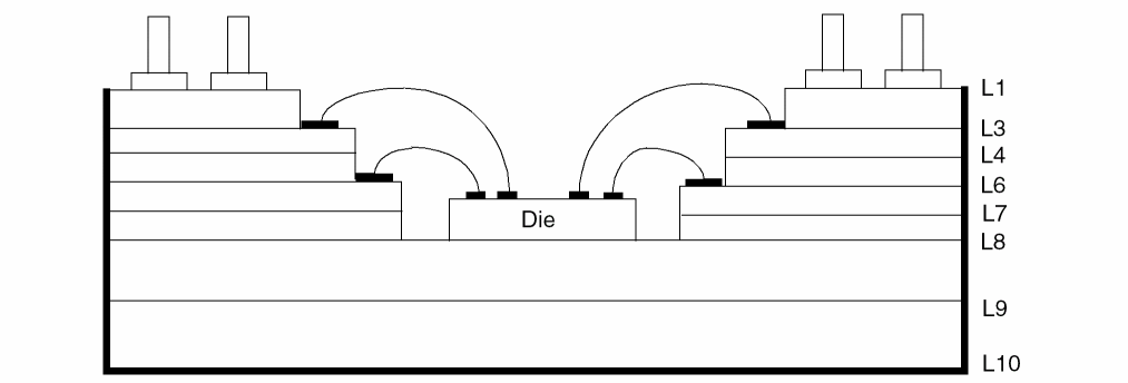
The stackup also provides the z-axis aspect of the electrical design, allowing for accurate positioning of conductive trace layers, power/ground layers, bond wire information, I/O pin position, and z-axis connections between trace layers or to a power or ground plane.
Information required for stackup modeling includes:
Layer Thickness
The overall thickness of the component is usually known and should be specified within the mechanical detailed information. Thickness is based on the number of layers required for the design. For example, a component may require 8 layers: 2 routing and 6 power/ground. The total thickness is the thickness of the 9 dielectric layers plus 8 layers of conductive material.
Individual layer thicknesses can be derived from the manufacturing data supplied by the foundry. You enter thickness data when you define the layer stackup.
Layer Materials
You should, at this point, know which materials to use for each of the conductive and dielectric layers. Material type is important to define the electrical characteristics of the component. You define these characteristics by specifying the electrical conductivity, and dielectric constant. However, you should obtain the exact specifications for the material through the manufacturing foundry, check them against the ECAD tool-generated values, and tune them to the manufacturing specification.
Layer Type
You specify a layer type to define the purpose the layer serves in the component design. Dielectric, conductive, plane, and bond wire are the most commonly used layer types, however, your design may require others. The significance of the layer type to the ECAD system is to specify effects (shield planes, design rule checking, and manufacturing output) for signal analysis.
Related Topics
Return to top