Virtuoso FinFET Support
Virtuoso® Layout Suite incorporates full support for the use of optimized 16nm native SKILL® process design kits (PDKs). This enables innovative FinFET custom design flows by supporting FinFET-based devices and rules at every design stage, together with a robust set of productivity-enhancing Virtuoso capabilities for leading custom and analog design.
This document summarizes the new capabilities added to Virtuoso layout tools to enable the structured FinFET custom placement using module generators (modgens); complex auto-alignment, device snapping, and abutment of FinFET-based devices; advanced rule support for layout automation; and sophisticated fluid guard ring generation.
This user guide is aimed at developers and designers of integrated circuits and assumes that you are familiar with:
- The Virtuoso Studio design environment and application infrastructure mechanisms designed to support consistent operations between all Cadence® tools.
- The applications used to design and develop integrated circuits in the Virtuoso Studio design environment, notably, the Virtuoso Layout Suite.
- The Virtuoso Studio design environment technology file.
At advanced process nodes, CMOS technology is moving away from planar field-effect transistors (FETs) towards more advanced device structures that offer reduced leakage and better control over short channel effects. This has led to the development of multi-gate FETs also known as tri-gate FETs or FinFETs.
FinFETS use long, narrow fins fabricated on top of the substrate and surrounded by the gate on three sides. The fin pitch is typically the same for all devices and fins are surrounded by a fin boundary shape. The devices also come with new design rule checks that are required to ensure that device are correctly and legally placed.
This document provides an overview of the enhancements made to Virtuoso layout editing tools in order to support FinFET-based design. These include:
-
Updates to the technology file definitions to let you define snap patterns for each layer-purpose pair on which FinFET devices will be placed. These snap patterns help ensure that placement constraints are honored when FinFET devices are created or edited either manually or automatically in the layout canvas.
For more information, see Technology File Requirements for FinFET-based Design. -
Updates to Virtuoso Layout Suite L (Layout L) to let you display the fin grids in the layout canvas, as well as automatically snap shapes and design objects to these grids when they are created or moved around the canvas.
For more information on these features, see FinFET Support in Layout L. -
Updates to Virtuoso Layout Suite XL (Layout XL) to preserve any snap patterns during layout generation; to generate a place and route boundary that is correctly sized in relation to the fin grid; to automatically snap FinFET devices to the fin grid when generating devices in the layout canvas; and fold FinFET devices based on a specified number of fins rather than the transistor width used to fold conventional devices.
For more information, see FinFET Support in Layout XL. -
Updates to the Virtuoso Module Generator feature to snap modgens to the top-level snap pattern shape and to let you specify the number of fins required for dummy devices.
For more information, see FinFET Support in Modgens. -
Updates to the layout editor design rule driven (DRD) editing feature, which now supports the generation and placement of FinFET devices based on FinFET-specific spacing, width, and enclosure rules.
For more information, see FinFET Support in DRD Editing.
Technology File Requirements for FinFET-based Design
This section summarizes the technology file definitions required to support snap patterns in your design, along with the public SKILL functions provided to create and locate snap pattern definitions in your technology files.
Layer Definition Requirements
You must update your layer definitions to define a purpose for each fin boundary type you require. The purpose you define
-
Must have parent purpose "
annotation" - Must be a user-defined purpose; you cannot specify a Virtuoso system-reserved purpose
You do this in the techPurposes section of the technology file. For example:
layerDefinitions(
    techPurposes(
        (fb        1001 fb   'parent "annotation")
        (fbdummy   1002 fbd  'parent "annotation")
        (polygrid  1003 pg   'parent "annotation")
    ) ;techPurposes
) ;layerDefinitions
When the purpose is defined, you can reference it in the snap pattern definition.
Snap Pattern Definition Requirements
You define snap patterns in the layerRules section of the technology file. A snap pattern definition lets you store and access the attributes for snap pattern shapes on a specific fin boundary LPP.
The snapPatternDef syntax is as follows:
layerRules(
snapPatternDefs(
(name (tx_layer tx_purpose)
'stepg_step'stepDirection {"horizontal" | "vertical"}
['type {"local" | "global"} ]
['offsetg_offset]
['snappingLayers (l_snappingLayers)]
['trackWidthg_trackWidth]
)
) ;snapPatternsDefs
) ;layerRules
The attributes defined in a snap pattern definition are listed below. For more detailed syntax information and examples of snap pattern definitions, see
- Name, which must be unique
- Layer-purpose pair, which provides the link between the snap pattern definition in the technology file and the snap pattern shapes drawn in the design
- Step, which specifies the spacing between snap pattern tracks
- Step direction, which specifies the direction in which to create the snap pattern tracks, either horizontal (grid step is applied left to right) or vertical (grid step is applied from bottom to top)
-
Type, which can be
localorglobal
When snapping a shape to a snap pattern grid, snap pattern shapes whose snap pattern definition is of typelocalhave higher priority than those of typeglobal - Offset, which specifies the distance of the first snap pattern track from the lower (for vertical direction) or left (for horizontal direction) edge of the shape bounding box
- Snapping layers; shapes on these layers snap to the snap pattern tracks. Each snapping layer has the following attributes:
- Track width, which specifies the width of the physical shape that each track represents
With the snap pattern definition loaded for the design, you can draw a fin boundary in the layout canvas, and when you move parameterized cells, vias, shapes, or instances over this fin boundary, the layout editor automatically snaps the objects to the defined fin grid. For more information, see Snapping Objects to Local Snap Pattern Shapes.
Snap Pattern SKILL Functions
You can use the following public SKILL functions to create and find snap pattern definitions in your technology files:
- techCreateSnapPatternDef lets you create a snap pattern definition in the current technology file
- techFindSnapPatternDefByLP lets you find a snap pattern definition based on its layer purpose pair
- techFindSnapPatternDefByName lets you find a snap pattern definition by name
FinFET Support in Layout L
This section summarizes the enhancements made to Layout L to support FinFET devices in your design. These include mechanisms to let you display the snap pattern grid in the layout canvas; to specify that design objects are to be automatically snapped to that grid; and to quickly place objects manually without zooming in to the canvas.
- Display fins, fin boundaries, and snap patterns in the layout canvas and specify that objects are automatically snapped to the snap pattern grid. See Snapping Objects to Local Snap Pattern Shapes for more information.
- Snap objects to a global snap pattern grid. See Snapping Objects to the Global Snap Pattern Grid for more information.
- Display snap patterns in the Palette assistant. See Controlling the Display of the Snap Pattern in the Palette for more information.
- Use Abstract Mode placement to improve performance when placing large blocks. See Modes for Object Placement for more information.
You customize the Create Guard Ring form to support advanced node design methodologies. For more information, see:
Snapping Objects to Local Snap Pattern Shapes
Layout L has been enhanced to let you display fin grids in the layout canvas and automatically snap design objects to these grids when the object is moved over the fin boundary LPP. For more information, see the following topics in the Virtuoso Layout Suite L User Guide.
- Controlling the Display of Snap Patterns
- Turning On Snap Pattern Snapping
- Object Snapping
- Group Snapping
Snapping Objects to the Global Snap Pattern Grid
The layout editor can now display a uniform fin grid called a global snap pattern grid that extend over the entire design window. You can use the global grid to
-
Snap local fin boundaries by adding the fin boundary LPP to the list of
snappingLayersfor the global snap pattern definition -
Snap Active shapes by adding the Active LPP to the list of
snappingLayersfor the global snap pattern definition
You create a global snap pattern grid by specifying the value global in the type constraint of the snap pattern definition, as shown below:
snapPatternDefs(
    (GFG ("CellBoundary" "global")
         'offset     0.024
         'step       0.048
         'type       "global"
         ...
You activate the global grid either through a constraint (snapGridVertical or snapGridHorizontal) or by drawing a corresponding snap pattern shape in the canvas.
Controlling the Display of the Snap Pattern in the Palette
You control the visibility of local and global snap pattern grids on the Grids panel of the Palette assistant.
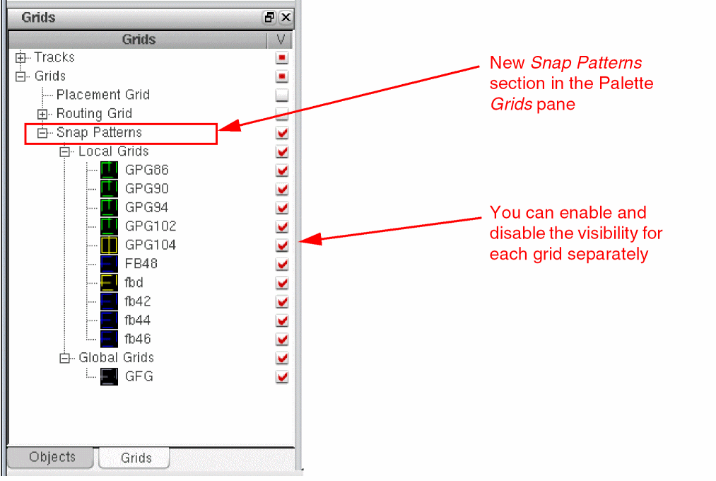
The grid drawing style is controlled through the Snap Pattern Display field in the Display Options form.
For more information, see
Modes for Object Placement
For small FinFET devices, placement is performed by searching the instance master for fin grids. If no fin grids are found, the snapping shapes are searched. This functionality is referred to as Detail Mode Placement.
When placing large blocks it is not feasible to search through instance masters and snapping shapes. Instead, Cadence recommends that you use Abstract Mode Placement, which allows fast placement of large layout blocks. In Abstract Mode, an instance snaps to a global snap pattern grid using either its snap boundary or PR boundary, or – if neither is found – the instance origin axis. For more information, see
There may also be situations where neither Detail Mode or Abstract Mode are appropriate; for example, when the design has a third-party IP block laid out using a different methodology. In these cases, you can use the Manual Mode Placement Override to manually specify the placement mode or offset on a per instance or per master basis. You do this by setting the leSnapPatternSnapping property on either the instance or the master concerned. For more information, see
SKILL Function for Fin Grid Snapping
A new dbMoveFig, and helps ensure that objects are placed legally after the move is complete.
Customizing the Create Guard Ring Form
When working at advanced node and advanced nodes methodologies, some system-defined GUI components available on the Create Guard Ring form might not be applicable. In such circumstances, you can customize the Create Guard Ring form to display user-defined widgets that let you use fluid guard rings for your specific design needs. Virtuoso provides some triggers and SKILL API functions specifically designed for this purpose. For more information, see
FinFET Support in Layout XL
This section summarizes the enhancements made to Layout XL to support FinFET devices in your design. These include the provision of new NFIN and PFIN component type attributes in CPH and the LAM file and the enhancement of the folding engine to support folding of FinFET devices. There is also support for snapping during the generation and editing of FinFET devices in the layout canvas and for generating a constraint-driven PR boundary.
Component Type Definition for FinFET Devices
For FinFET devices to be recognized by layout generation commands such as Generate All From Source and for these devices to support operations such as chaining and folding, they must be assigned to an appropriate component type—PFIN or NFIN. You define these component types and assign devices to them using either:
- The Configure Physical Hierarchy command. See Component Types Mode for more information.
- The library and attributes mapping (LAM) file. See LAM File Component Type Section for more information.
Generating a Constraint-Driven PR Boundary
The Generate All From Source and Update Components And Nets commands now generate a PR boundary with dimensions based on a new allowedPRBoundaryDimensions constraint, which ensures that the PR boundary is legal for use in FinFET-based designs.
The constraint has the following syntax:
spacings(
(allowedPRBoundaryDimensions
['vertical | 'horizontal]
['stepSizeg_step] (g_ranges)
)
);spacings
The allowedPRBoundaryDimensions constraint can be applied separately for the horizontal and vertical directions to cover all the dimensions of a PR boundary.
Preserving Snap Patterns and Generating Devices
Generate All From Source now features an option to preserve any Snap Patterns already defined in the layout view. See
Layout XL now also correctly snaps FinFET devices to the fin grid defined for the design in the following scenarios:
- When placing FinFET devices in your layout using the Generate Selected From Source command in Group As In Schematic mode, the generated devices are automatically snapped to the fin grid.
- When moving a chain of abutted devices in the layout canvas, all the devices in the chain are snapped together (i.e., the snapping does not break any existing chains).
Folding FinFET Devices
Folding lets you divide an individual device or a chain of devices into two or more layout instances with terminals connected in parallel to the same nets. The aim is to change the aspect ratio of the devices in your design while retaining the original orientation and design intent of the device that was folded.
To enable folding for FinFET devices, the devices in question must have their component classes correctly defined as either NFIN or PFIN as described above. See
Additionally, the Number of fins parameter or the Width parameter must be set in the folding form. For more information, see Folding a Transistor in the Virtuoso Layout Suite XL User Guide.
FinFET Support in Modgens
The Module Generator feature has also been enhanced to support FinFET-based design.
Snapping Modgens
Because the layout editor has been enhanced to automatically snap the parameterized cells in modgens to the snap pattern, the entire modgen block is also snapped to the top-level snap pattern shape.
Additionally, the modgen
FinFET Support in DRD Editing
Design rule driven editing now supports the creation and placement of FinFET devices that adhere to FinFET-specific spacing, width, and enclosure rules:
-
Use the
allowedSpacingRangesconstraint to define legal spacing rules in the form of ranges and discrete values. See Defining Discrete Spacing Rules. -
Use the
minSpacingconstraint with derived layers to define the minimum spacings between fin boundaries. See Defining Minimum Spacing Rules. -
Use the
allowedWidthRangesconstraint to define directional legal width rules in the form of ranges and discrete values. See Defining Directional and Discrete Width Rules. -
Use the
allowedPRBoundaryDimensionsandminPRBoundaryInteriorHaloconstraints to define directional legal spacing and width rules for PR boundaries. See Defining Directional and Discrete P&R Boundary Rules. -
Use the
minOppExtensionconstraint to define directional and discrete enclosure rules for overlapping shapes on two different layers. See Defining Directional and Discrete Opposite Extension Rules.
For more information on these features, see
Return to top