Subthreshold Current
There are two subthreshold current models that you can select with the subthmod parameter. If you set subthmod to 0, none of the subthreshold current models are used. For example, the drain current is zero when the gate voltage is less than the threshold voltage. If you set subthmod to 1, the summation approach is used. For example, the subthreshold current is always calculated and added to the drain current for the strong-inversion region, regardless of the operating region.
If you set subthmod to 2, a transition region between the subthreshold regions and the strong-inversion regions is created. This transition region provides smooth switching between the subthreshold and the strong-inversion regions. The following equations are model equations for the subthreshold and transition regions.
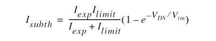
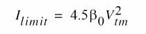
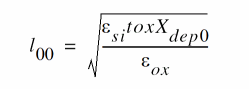
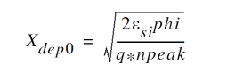
subthmod = 1
(-7)
where
(-8)
(-9)

(-10)

(-11)

(-12)

(-13)
(-14)
(-15)

(-16)
(-17)
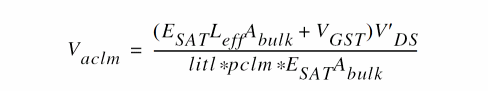
subthmod = 2
If VGST ≤ Vglow – Vdibl, the drain current is given by current.
(-18)

If Vglow – Vdibl ≤ VGST ≤ Vghigh + Vdibl, the device is operated in the transition region and the drain current is given by
(-19)

where Idlow is the subthreshold current evaluated at VGST = Vglow –Vdibl, and Idhigh is the strong-inversion drain current evaluated at VGST = Vghigh + Vdibl.
(-20)
(-21)

(-22)

(-23)

gmhigh and gmlow are the transconductances evaluated at VGST = Vghigh + Vdibl.
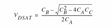
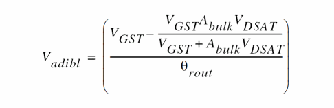
Drain Saturation Voltage
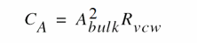
If Rds = 0,
(-24)
otherwise
(-25)
where
(-26)
(-27)
(-28)
(-29)

If keta = 0,
(-30)
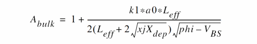
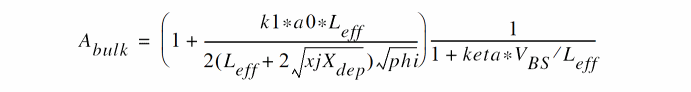
otherwise,
(-31)
(-32)
(-33)

(-34)

(-35)

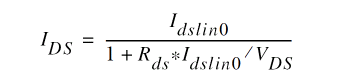
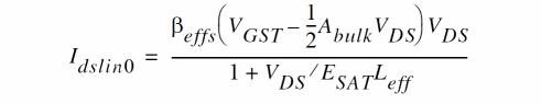
Drain Current for the Triode Region
(-36)
 \
\
where Idslin0 is the drain current in the triode region without the presence of source and drain parasitic resistance.
(-37)
(-38)
Drain Current for the Saturation Region
(-39)

where
(-40)

(-41)
satmod = 1
(-42)

(-43)

satmod = 2
(-44)
(-45)
(-46)
where
(-47)

Default Model Parameter Value Calculation
The following are the calculation methods for default model parameter values under various conditions:
-
If vtho is not given, it is calculated from
(-48)

-
If phi is not given, it is calculated from
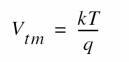
(-49)
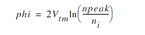
where Vtm is the thermal voltage given by
(-50)
(-51)
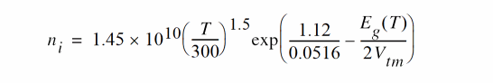
where Eg(T) is the energy band gap at temperature T. The equation for Eg is shown in BSIM3v2 Level-10 Model (bsim3)
-
If k1 is not given, it is calculated from
(-52)

-
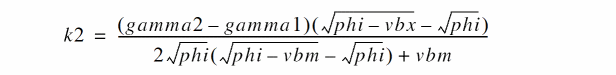
If k2 is not given, it is calculated from
(-53)
-
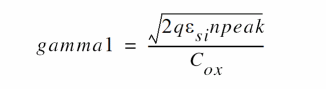
If gamma1 is not given, it is calculated from
(-54)
-
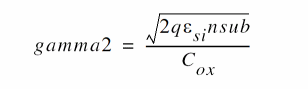
If gamma2 is not given, it is calculated from
(-55)
-
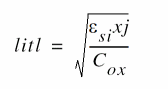
If litl is not given, it is calculated from
(-56)
-
If vtho is not given, vfb is always calculated from
(-57)

regardless of any value you specify.
-
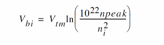
If Vbi is not given, it is calculated from
(-58)
-
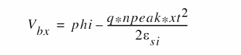
If Vbx is not given, it is calculated from
(-59)
-
If gamma1 is given, npeak is calculated from
(-60)
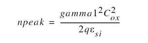
regardless of any value you specify.
If neither gamma1 nor npeak is specified, npeak defaults to 1.7e1.7, and gamma1 is calculated from npeak.
-
The default value for uo is 670 cm2/V sec for NMOS and 250 cm2/V sec for PMOS.
-
The temperature-dependent mobility is calculated as
(-61)
-
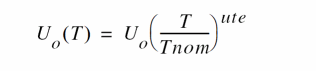
The temperature-dependent saturation velocity is calculated as
(-62)

-
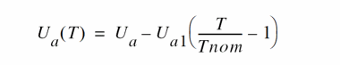
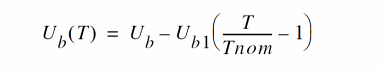
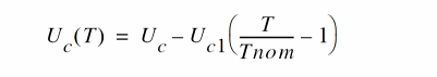
The temperature-dependent mobility degradation parameters are calculated as
(-63)
(-64)
(-65)
-
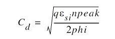
If Vghigh is not given, it is calculated from
(-66)
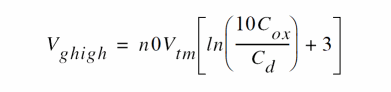
where
(-67)
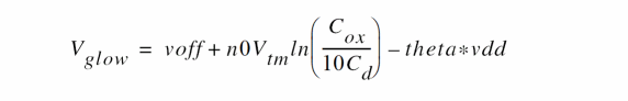
-
If Vglow is not given, it is calculated from
(-68)
-
If cgdo(cgso) is not given, it is calculated from
(-69)
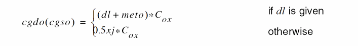
Also, if cgdo(cgso) is zero, 10-7 x Cox is used.
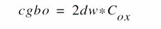
If cgbo is not given, it is calculated from
(-70)
Scaling Effects
For more information about scaling effects, seeScaling Factors (scale and scalem).
New Features in BSIM3 Version 3.2.4
The following features have been added to BSIM3v3.2.4:
-
A Spectre circuit simulator thermal noise model with the noise coefficient varying smoothly between 4 to 8/3 when the device moves from linear region to saturation region.
-
A BSIM4 ACNQS model that enables the NQS effect in AC simulations.
-
A new parameter lintnoi introducing an offset to the length reduction parameter (lint) to improve the accuracy of the flicker noise model
With the capacitance bug fix in this version, the transcapacitance CGG for capmod=3 is now smooth from the subthreshold region to strong inversion with no negative value.
BSIM3v3.2.4 is backward compatible with the previous versions of the model.
Component Statements
This device is supported within altergroups.
Sample Instance Statement:
m3 (1 2 0 0) nchmod l=1.5u w=100u as=450p ad=450p pd=209u ps=209u nrd=207m nrs=207m m=1
Sample Model Statement:
model nchmod bsim3 vtho=5.94e-01 phi=0.69 k1=0.72 k2=0 w0=1.3e-07 tox=5.9e-09 rdsw=80 uo=499 xj=2e-07 vsat=600e+04 at=3.4e+04 a0=0.8 cdsc=1.4e-03 nfactor=1.03
Instance Syntax
Name d g s b ModelName parameter=value ...
Instance Parameters
|
w
|
(m)
|
Channel width.
|
|
l
|
(m)
|
Channel length.
|
|
as
|
(m2)
|
Area of source diffusion.
|
|
ad
|
(m2)
|
Area of drain diffusion.
|
|
ps
|
(m)
|
Perimeter of source diffusion.
|
|
pd
|
(m)
|
Perimeter of drain diffusion.
|
|
nrd
|
(m/m)
|
Number of squares of drain diffusion.
|
|
nrs
|
(m/m)
|
Number of squares of source diffusion.
|
|
isnoisy
|
yes
|
Should device generate noise.Possible values are no and yes.
|
|
m
|
1
|
Multiplicity factor (number of MOSFETs in parallel).
|
|
region
|
triode
|
Estimated operating region. Spectre generates output number (0-4) in a rawfile.Possible values are off, triode, sat, subth and breakdown.
|
|
trise
|
|
Temperature rise from ambient.
|
|
geo
|
0
|
Geometry selector.
|
Model Syntax
model modelName bsim3 parameter=value ...
Model Parameters
Device type parameters
|
type
|
n
|
Transistor type.Possible values are n and p.
|
Threshold voltage parameters
|
vtho
|
0 V
|
Threshold voltage at zero body bias.
|
|
phi
|
0.7 V
|
Surface potential at strong inversion.
|
|
k1
|
0.53 V
|
Body-effect coefficient.
|
|
k2
|
-0.0186
|
Charge-sharing parameter.
|
|
k3
|
80
|
Narrow width coefficient.
|
|
k3b
|
0 1/V
|
Narrow width coefficient.
|
|
w0
|
2.5e-6 m
|
Narrow width coefficient.
|
|
nlx
|
1.74e-7 m
|
Lateral nonuniform doping coefficient.
|
|
gamma1
|
0 V
|
Body-effect coefficient near the surface.
|
|
gamma2
|
0 V
|
Body-effect coefficient in the bulk.
|
|
theta
|
0.02 1/V
|
Drain-induced barrier lowering coefficient.
|
|
eta
|
0.3 1/V
|
Effective drain voltage coefficient.
|
|
litl
|
(m)
|
Depth of current path.
|
|
vfb
|
-1.0 V
|
Flat-band voltage.
|
|
vbx
|
(V)
|
Threshold voltage transition body voltage.
|
|
vbi
|
(V)
|
Substrate junction built-in potential.
|
|
vbm
|
-5 V
|
Maximum applied body voltage.
|
|
dvt0
|
2.2
|
First coefficient of short-channel effects.
|
|
dvt1
|
0.53
|
Second coefficient of short-channel effects.
|
|
dvt2
|
-0.032 1/V
|
Body-bias coefficient of short-channel effects.
|
|
a0
|
1 for nmos and 4.4 for pmos
|
Nonuniform depletion width effect coefficient.
|
|
a1
|
0 for nmos, 0.23 for pmos
|
No-saturation coefficient.
|
|
a2
|
1 for nmos, 0.08 for pmos
|
No-saturation coefficient.
|
|
keta
|
-0.047 1/V
|
Body-bias coefficient for non-uniform depletion width effect.
|
Process parameters
|
nsub
|
2e15 cm-3
|
Substrate doping concentration.
|
|
npeak
|
1.7e17 cm-3
|
Peak channel doping concentration.
|
|
ngate
|
(cm-3)
|
Poly-gate doping concentration.
|
|
xj
|
0.15e-6 m
|
Source/drain junction depth.
|
|
dl
|
0 m
|
Lateral diffusion for one side.
|
|
dw
|
0 m
|
Width reduction for one side.
|
|
tox
|
1.5e-8 m
|
Gate oxide thickness.
|
|
vdd
|
5 V
|
Maximum drain voltage.
|
|
xt
|
1.55e-7 m
|
Doping depth.
|
|
ldd
|
0 m
|
Total length of lightly doped drain region.
|
|
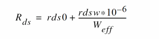
rds0
|
0 Ω
|
Total drain-source resistance.
|
|
rdsw
|
0 Ω μm
|
Width dependence of drain-source resistance.
|
Mobility parameters
|
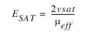
uo
|
670 cm2/V s
|
Low-field surface mobility at tnom. Default is 250 for PMOS.
|
|
vsat
|
9.58e4 m/s
|
Carrier saturation velocity at tnom.
|
|
ua
|
2.25e-9 m/v
|
First-order mobility reduction coefficient.
|
|
ub
|
5.87e-19 m2/v2
|
Second-order mobility reduction coefficient.
|
|
uc
|
0.0465 1/V
|
Body-bias dependence of mobility.
|
|
uc0
|
0
|
Mobility coefficient.
|
Output resistance parameters
|
satmod
|
2
|
Saturation model selector.
|
|
bulkmod
|
1
|
Bulk-charge effect model selector.
|
|
drout
|
0.56
|
DIBL effect on output resistance coefficient.
|
|
alpha
|
1.9
|
Reference voltage multiplication factor.
|
|
em
|
4.1e7 V/m
|
Maximum electric field.
|
|
pclm
|
1.3
|
Channel length modulation coefficient.
|
|
pdibl1
|
0.39
|
First coefficient of drain-induced barrier lowering.
|
|
pdibl2
|
8.6e-3
|
Second coefficient of drain-induced barrier lowering.
|
|
pscbe1
|
4.24e8 V/m
|
First coefficient of substrate current body effect.
|
|
pscbe2
|
1e-5 m/v
|
Second coefficient of substrate current body effect.
|
|
pvag
|
0
|
Gate dependence of Early voltage.
|
Subthreshold parameters
|
subthmod
|
2
|
Subthreshold model selector.
|
|
vghigh
|
0.12 V
|
Upper bound of transition region.
|
|
vglow
|
-0.12 V
|
Lower bound of transition region.
|
|
cdsc
|
2.4e-4 F/m2
|
Source/drain and channel coupling capacitance.
|
|
cdscb
|
0 F/m2 V
|
Body-bias dependence of cdsc.
|
|
nfactor
|
1
|
Subthreshold swing coefficient.
|
|
cit
|
0 F
|
Interface trap parameter for subthreshold swing.
|
|
voff
|
-0.11 V
|
Threshold voltage offset.
|
|
dsub
|
drout
|
DIBL effect in subthreshold region.
|
|
eta0
|
0.08
|
DIBL coefficient subthreshold region.
|
|
etab
|
-0.07 1/V
|
Body-bias dependence of et0.
|
Parasitic resistance parameters
|
rsh
|
0 Ω/sqr
|
Source/drain diffusion sheet resistance.
|
|
rs
|
0 Ω
|
Source resistance.
|
|
rd
|
0 Ω
|
Drain resistance.
|
|
lgcs
|
0 m
|
Gate-to-contact length of source side.
|
|
lgcd
|
0 m
|
Gate-to-contact length of drain side.
|
|
rsc
|
0 Ω
|
Source contact resistance.
|
|
rdc
|
0 Ω
|
Drain contact resistance.
|
|
rss
|
0 Ω m
|
Scalable source resistance.
|
|
rdd
|
0 Ω m
|
Scalable drain resistance.
|
|
sc
|
infinity m
|
Spacing between contacts.
|
|
ldif
|
0 m
|
Lateral diffusion beyond the gate.
|
|
hdif
|
0 m
|
Length of heavily doped diffusion.
|
|
minr
|
0.1 Ω
|
Minimum source/drain resistance.
|
Junction diode model parameters
|
js
|
(A/m2)
|
Bulk junction reverse saturation current density.
|
|
is
|
1e-14 A
|
Bulk junction reverse saturation current.
|
|
n
|
1
|
Junction emission coefficient.
|
|
dskip
|
yes
|
Use simple piece-wise linear model for diode currents below 0.1*iabstol.Possible values are no and yes.
|
|
imelt
|
`imaxA'
|
Explosion current.
|
|
jmelt
|
`jmaxA/m'2
|
Explosion current density.
|
Overlap capacitance parameters
|
cgso
|
(F/m)
|
Gate-source overlap capacitance.
|
|
cgdo
|
(F/m)
|
Gate-drain overlap capacitance.
|
|
cgbo
|
(F/m)
|
Gate-bulk overlap capacitance.
|
|
meto
|
0 m
|
Metal overlap in fringing field.
|
Junction capacitance model parameters
|
cbs
|
0 F
|
Bulk-source zero-bias junction capacitance.
|
|
cbd
|
0 F
|
Bulk-drain zero-bias junction capacitance.
|
|
cj
|
5e-4 F/m2
|
Zero-bias junction bottom capacitance density.
|
|
mj
|
1/2
|
Bulk junction bottom grading coefficient.
|
|
pb
|
0.8 V
|
Bulk junction built-in potential.
|
|
fc
|
0.5
|
Forward-bias depletion capacitance threshold.
|
|
cjsw
|
5e-10 F/m
|
Zero-bias junction sidewall capacitance density.
|
|
mjsw
|
1/3
|
Bulk junction sidewall grading coefficient.
|
|
pbsw
|
0.8 V
|
Side-wall junction built-in potential.
|
|
fcsw
|
0.5
|
Side-wall forward-bias depletion capacitance threshold.
|
Charge model selection parameters
|
capmod
|
yang
|
Intrinsic charge model.Possible values are none, meyer, yang and bsim.
|
|
xpart
|
1
|
Drain/source channel charge partition in saturation for BSIM charge model, use 0.0 for 40/60, 0.5 for 50/50, or 1.0 for 0/100.
|
|
xqc
|
0
|
Drain/source channel charge partition in saturation for charge models, e.g. use 0.4 for 40/60, 0.5 for 50/50, 0 for 0/100.
|
Default instance parameters
|
w
|
5e-6 m
|
Default channel width.
|
|
l
|
5e-6 m
|
Default channel length.
|
|
as
|
0 m2
|
Default area of source diffusion.
|
|
ad
|
0 m2
|
Default area of drain diffusion.
|
|
ps
|
0 m
|
Default perimeter of source diffusion.
|
|
pd
|
0 m
|
Default perimeter of drain diffusion.
|
|
nrd
|
0 m/m
|
Default number of squares of drain diffusion.
|
|
nrs
|
0 m/m
|
Default number of squares of source diffusion.
|
Temperature effects parameters
|
tnom
|
(C)
|
Parameters measurement temperature. Default set by options.
|
|
trise
|
0 C
|
Temperature rise from ambient.
|
|
tlev
|
0
|
DC temperature selector.
|
|
tlevc
|
0
|
AC temperature selector.
|
|
eg
|
1.12452 V
|
Energy band gap.
|
|
gap1
|
7.02e-4 V/C
|
Band gap temperature coefficient.
|
|
gap2
|
1108 C
|
Band gap temperature offset.
|
|
kt1
|
-0.11 V
|
Temperature coefficient for threshold voltage.
|
|
kt1l
|
-1.86e-7 v m
|
Temperature coefficient for threshold voltage.
|
|
kt2
|
0.022
|
Temperature coefficient for threshold voltage.
|
|
at
|
3.3e4 m/s
|
Temperature coefficient for vsat.
|
|
ua1
|
4.31e-9 m/v
|
Temperature coefficient for ua.
|
|
ub1
|
-7.61e-18 m2/v2
|
Temperature coefficient for ub.
|
|
uc1
|
-0.056 1/V
|
Temperature coefficient for uc.
|
|
trs
|
0 1/C
|
Temperature parameter for source resistance.
|
|
trd
|
0 1/C
|
Temperature parameter for drain resistance.
|
|
ute
|
-1.5
|
Mobility temperature exponent.
|
|
xti
|
3
|
Saturation current temperature exponent.
|
|
ptc
|
0 V/C
|
Surface potential temperature coefficient.
|
|
tcv
|
0 V/C
|
Threshold voltage temperature coefficient.
|
|
pta
|
0 V/C
|
Junction potential temperature coefficient.
|
|
ptp
|
0 V/C
|
Sidewall junction potential temperature coefficient.
|
|
cta
|
0 1/C
|
Junction capacitance temperature coefficient.
|
|
ctp
|
0 1/C
|
Sidewall junction capacitance temperature coefficient.
|
Noise model parameters
|
noisemod
|
1
|
Noise model selector.
|
|
kf
|
0
|
Flicker (1/f) noise coefficient.
|
|
af
|
1
|
Flicker (1/f) noise exponent.
|
|
ef
|
1
|
Flicker (1/f) noise frequency exponent.
|
|
wnoi
|
1e-5 m
|
Channel width at which noise parameters were extracted.
|
|
a
|
1e16 for nmos and 9.9e14 for pmos
|
Oxide trap density coefficient.
|
|
b
|
5e4 for nmos and 2.4e3 for pmos
|
Oxide trap density coefficient.
|
|
c
|
-1.4e-8 for nmos and 1.4e-8 for pmos
|
Oxide trap density coefficient.
|
Operating region warning control parameters
|
alarm
|
none
|
Forbidden operating region.Possible values are none, off, triode, sat, subth and rev.
|
|
imax
|
1 A
|
Maximum allowable current.
|
|
jmax
|
1e8 A/m2
|
Maximum allowable current density.
|
|
bvj
|
infinity V
|
Junction reverse breakdown voltage.
|
|
vbox
|
1e9*tox V
|
Oxide breakdown voltage.
|
|
maxvp
|
1.12 V
|
Maximum allowable voltage across the gate poly layer.
|
Compatibility model parameters
|
compatible
|
spectre
|
Encourage device equations to be compatible with a foreign simulator. This option does not affect input syntax.Possible values are spectre, spice2, spice3, cdsspice, hspice, spiceplus, eldo, sspice, mica, tispice and pspice.
|
Auto Model Selector parameters
|
wmax
|
1.0 m
|
Maximum channel width for which the model is valid.
|
|
wmin
|
0.0 m
|
Minimum channel width for which the model is valid.
|
|
lmax
|
1.0 m
|
Maximum channel length for which the model is valid.
|
|
lmin
|
0.0 m
|
Minimum channel length for which the model is valid.
|
Junction model
|
acm
|
12
|
Junction area calculation method selector.
|
|
jsw
|
0.0 A/m
|
Sidewall bulk junction saturation current density.
|
|
nds
|
1.0
|
Reverse bias slope coefficient.
|
|
vnds
|
-1.0 V
|
Reverse diode current transition point.
|
|
cjgate
|
`cjswF/m'
|
Zero bias gate-edge sidewall bulk junction capacitance density.
|
|
php
|
pb V
|
Bulk junction sidewall contact potential.
|
|
tt
|
0.0 s
|
Transit time.
|
|
ld
|
(m)
|
Lateral diffusion into the channel from the source and drain diffusion.
|
|
wmlt
|
1.0
|
Width diffusion layer shrink reduction factor.
|
|
ijth
|
1.0 A
|
Explosion current.
|
Imax and Imelt:
The imax parameter aids convergence and prevents numerical overflow. The junction characteristics of the device are accurately modeled for current up to imax. If imax is exceeded during iterations, the linear model is substituted until the current drops below imax or until convergence is achieved. If convergence is achieved with the current exceeding imax, the results are inaccurate, and Spectre prints a warning.
A separate model parameter, imelt, is used as a limit warning for the junction current. This parameter can be set to the maximum current rating of the device. When any component of the junction current exceeds imelt, the base and collector currents are composed of many exponential terms, Spectre issues a warning and the results become inaccurate. The junction current is linearized above the value of imelt to prevent arithmetic exception, with the exponential term replaced by a linear equation at imelt.
Both of these parameters have current density counterparts, jmax and jmelt, that you can specify if you want the absolute current values to depend on the device area.
Auto Model Selection:
Many models need to be characterized for different geometries in order to obtain accurate results for model development. The model selector program automatically searches for a model with the length and width range specified in the instance statement and uses this model in the simulations.
For the auto model selector program to find a specific model, the models to be searched should be grouped together within braces. Such a group is called a model group. An opening brace is required at the end of the line defining each model group. Every model in the group is given a name followed by a colon and the list of parameters. Also, the four geometric parameters lmax, lmin, wmax, and wmin should be given. The selection criteria to choose a model is as follows:
lmin <= inst_length < lmax and wmin <= inst_width < wmax
Example:
model ModelName ModelType {
1: <model parameters> lmin=2 lmax=4 wmin=1 wmax=2
2: <model parameters> lmin=1 lmax=2 wmin=2 wmax=4
3: <model parameters> lmin=2 lmax=4 wmin=4 wmax=6
}
Then for a given instance
M1 1 2 3 4 ModelName w=3 l=1.5
the program would search all the models in the model group with the name ModelName and then pick the first model whose geometric range satisfies the selection criteria. In the preceding example, the auto model selector program would choose ModelName.2.
You must specify both length (l) and width (w) on the device instance line to enable automatic model selection.
Output Parameters
|
weff
|
(m)
|
Effective channel width.
|
|
leff
|
(m)
|
Effective channel length.
|
|
rseff
|
(Ω)
|
Effective source resistance.
|
|
rdeff
|
(Ω)
|
Effective drain resistance.
|
Related Topics
MOS Level-2 Model (mos2)
MOS Level-3 Model (mos3)
BSIM1 Level-4 Model (bsim1)
BSIM2 Level-5 Model (bsim2)
Return to top