1
Setting up the Interactive Routing Environment

If you choose not to use automatic routing, you can manually (or interactively) route the connections in your design. The interactive routing features complement automatic routing features. Interactive routing lets you do the following:
- complete critical nets before automatic routing.
- finish incomplete nets left after automatic routing.
The Virtuoso® Interactive and Assisted Routing capabilities enable you to route connections interactively within the Virtuoso environment. These capabilities provide efficient ways to interactively and automatically route connections in order to meet critical design constraints and rules. The interactive and assisted routing capabilities are fully enabled on all process nodes including the most advanced process technologies.
In this chapter we are going to explore the settings that can modify and change the behavior and functionalities of the interactive and assisted routing commands.
The chapter describes the following,
- Configuring Wire Editing Options
- Tapping Wires
- Adding the lxStickyNet Property to Wires
- Support for Voltage-Dependent Rules
- Support for Area-based Rules
- Using Mouse Button Controls
- Startup Warnings
License Requirements of Interactive Routing Features
The Interactive wire editing features use the token-based license scheme under the Layout XL and higher tier licenses. The following table lists the features and the layout levels at which each is available.
|
The Create Geometric Wire command is available by default in CIW using a SKILL API leHiCreateGeometricWire. In addition, to add the Create Geometric Wire to the Create – Wiring menu, set the mixedSignalWireEditingEnvironment
|
||
* This license level offers a subset of feature functionality.
For information about licensing in the Virtuoso Studio design environment, see Virtuoso Software Licensing and Configuration Guide.
Configuring Wire Editing Options
You can configure wire editing options to control the way the wire editor behaves as well as how it generates vias. You can set up wire editing options in:
Layout Editor Options Form
Choose Options – Editor to open the Point to Point Form. The fields relevant for creating and editing wires include options in the Snapping, Tap, Wire Editing, and Halo sections.
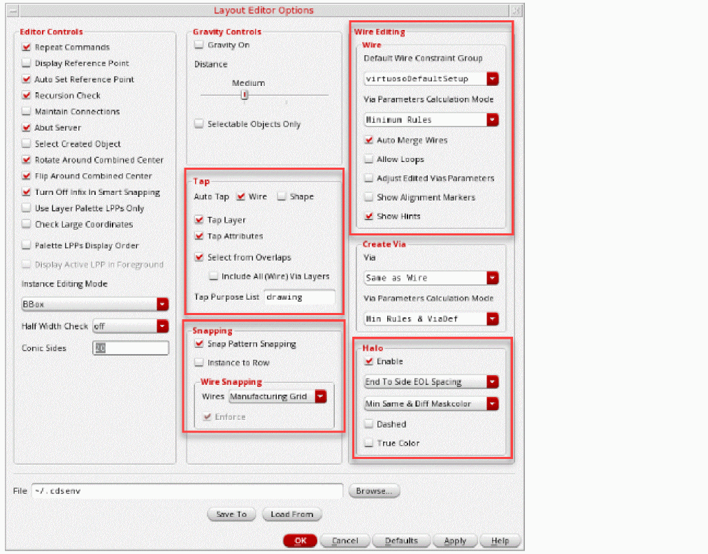
The Default Wire Constraint Group drop-down list box in the Wire Editing section allows the selection of one of the available constraint groups, which may be defined at the technology or the design level. By default, the Default Wire Constraint Group cyclic field displays a list of all available constraint groups. However, when the environment variable is set to t, the Default Wire Constraint Group cyclic field displays a customized list of constraint groups. Only the constraint groups for which the custom API constraintGroupCustomFilter returns t are displayed. The constraint group defines the appropriate layers and vias for the application being used. Only the layers, vias, and any rules specified in the selected constraint group are used when creating wires. Selection of a constraint group in the Default Wire Constraint Group drop-down list box specifies the application default constraint group for wire creation and editing commands.
To override constraints in the application default constraint group at the design level,
- Create a new design constraint group.
- Inherit the application constraint group in the design constraint group.
- Add new constraints (the ones that you need to override) in front of the linked application constraint group.
- Select the new design constraint group as the application default constraint group in the Default Wire Constraint Group drop-down list box.
All container objects in the database have a default constraint group associated with them. Creating a rule override directly on a net or on the design requires adding that rule to the default constraint group of the net or the design. CST is the constraint look-up mechanism to determine the precedence of constraints applied at various levels. The precedence order followed by the router is:
Related Topics
Stretch Options
In Virtuoso Layout Suite, logical connectivity is not taken into account when stretching wires. If DRD is on, DRD uses logical connectivity to flag or avoid shorts. Choose Edit – Stretch to open the Metal Density Options Form.
For the stretch command, there is no initial check for constraints. The constraint check depends on whether the constraintAwareEditing environment variable is ON or OFF. If it is ON, you can create a bus and check the constraints on each net. However, if it OFF, create a set of wires and do not check the minSpacing constraints.
This is recommended for the interactive routing commands to improve the runtime and also the use model.
In addition, in the Configure tab of the Connectivity form, you can deselect the Constraint-aware editing option.
Related Topics
Tapping Wires
For a description of the Layout Editor Tap options, see Point to Point Form.
For more information about selecting the starting and target object layers, without tapping an object, see Smart Snapping in Interactive and Assisted Routing Commands.
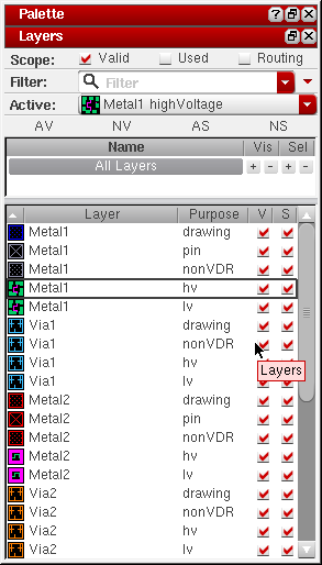
When creating a wire, layers can be selected by clicking on an LPP in the Layers Assistant or by tapping on objects. You can select to tap the objects layer and/or attributes. In the Layout XL or higher applications, in addition to object attributes, an existing net name can be tapped. To disable the layer tapping, hold the Shift or the Ctrl key.
There are two different tap options, one is used when creating shapes and the other is used when creating wires.
-
Options – Layout Editor – Auto Tap –- Wire
Turning on Auto Tap – Wire will automatically tap an object’s layers and attributes when digitizing the first coordinate of a wire. Layers that can be tapped are determined from the technology file.
When two or more layers are tapped, the Choose Object to Tap From form is displayed. However, when one of the tapped layers is already selected in Layers Assistant, it prevents displaying the Choose Object to Tap From form. For more information, refer to Point to Point Form.
When using the Layout L editor, available layers are determined from theviaDefsstatement. When using the Layout XL editor and higher tiers, valid routing layers should be specified in a setup constraint group. When tapping an object, only layers specified in the setup constraint group can be tapped. -
Options – Layout Editor – Auto Tap – Shape
Turning on Auto Tap – Shape will automatically tap an object’s layers and attributes when digitizing the first coordinate of a rectangle, polygon, path, circle, donut, and ellipse. All layers can be tapped.
To tap an object or automatically set the layer when digitizing the first coordinate of a wire on an existing wire or object, turn on Auto Tap – Wire in the Layout Editor Options form.
The level of hierarchy that you are allowed to tap is dependent on the Display Levels set in the Display Options form.
To tap specific layers purposes, create a prioritized list through the Tap Purpose List on the Layout Options form, or through the environment variables, useTapPurposeList and tapPurposeList. The default purpose is drawing, which can be overridden through Tap Purpose List.
For example, when Tap Purpose List is:
-
The default purpose for
metal1isdrawing. -
When tapping an object on the LPP
metal1net, the active layer is changed tometal1net. -
When tapping an object on an LPP which is not listed the Tap Purpose List, such as
metal1pin, the active layer does not change. The last layer chosen remains the active layer.
Once you have chosen a purpose for a layer, whether through the LSW or through tapping an object, the purpose will be used for subsequent create commands. If the layer has not yet been used in the current command, the current purpose will be used.
Tapping Internal Nets
When tapping on a pin that is at a lower level of the hierarchy, the connectivity must be traceable to the top level in order for the connectivity to be applied. This corresponds to the MUST connect relationship.
In Example 1 below, the pin gnd! at level 2 in the hierarchy is connected to net gnd!. At the top level there is a net gnd! and a pin gnd! to which the lower level gnd! is connected. In this case tapping on the pin at level 2 in the hierarchy will return correct net information.
In Example 2 below, when tapping on one of the A pins in I1, which is connected by internal net net5, the net information cannot be traced to a top level term/instTerm. In this example, no net name will be given to the new object being created.
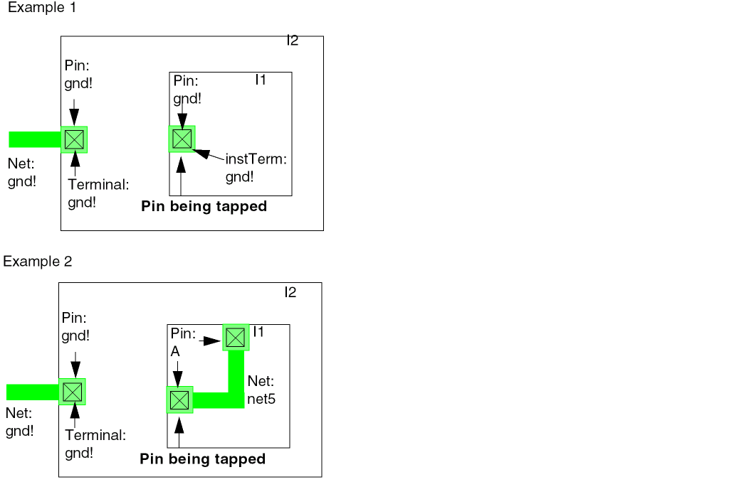
If a net information can not be traced up to a top level net, then warning messages will be output to the CIW. If the wire does not have a net name, the software is free to merge the wire to another wire that does not have a net name at the top level. The result of such merge may not be the desired results. Therefore, it is advisable to manually cancel out the command when warning 105200 or 1050201 messages appear.
When tapping is enabled, the net on the tapped shape is considered. Else, the net selected in the Navigator assistant, if any, is considered.
Tapping Vias
In Virtuoso L, when you click a via or a stacked via, you are prompted with the Choose object to tap from form to choose a layer from which to extend a wire from the via.
TRUE when smart snapping is disabled.In Virtuoso XL and higher tiers, when you click a via or a stacked via, if there is an existing segment connected to one layer of the via, the resulting layer tap will be on the unoccupied layer of the via. However, in some situations, you may want to tap on a via and create a T-junction, rather than extend a wire from a dangling end of a wire.
To change the default behavior of Virtuoso XL and higher tiers and be prompted with the Choose object to tap from form when tapping a via, do the following.
-
Select Options – Editor.
The Layout Editor Options form opens. - Select the Select from Overlaps and Include All (Wire) Via Layers check boxes.
The associated environment variables are:
envSetVal("layoutlayerTapPickWireVia" 'boolean t)
envSetVal("layoutlayerTapPick" 'boolean t)
Tapping Results Based on validVias and validLayers
When tapping on an object, any via listed in the validVias constraint can be placed in the design and the resulting wire will be started on a layer that is listed in the validLayers constraint.
For example, if the validLayers are M2 and M3, and the validVias are M1M2 and M3M4, when tapping on a M1 or M4 shape, you must choose between M1 and M4 even though the valid layers are M2 and M3. The router can drop either a M1M2 or M3M4 via because they are both listed in the validVias constraint and the resulting wire would be started on a valid layer. Layers are only auto selected when there is only one available option.
Stacked vias are also allowed. In the example above, if an M4M5 via was also included in the validVias, then tapping on an M5 shape would be allowed.
In the same example of validLayers being M2 and M3, if two shapes were overlapping, one on M3 and one on M4, then the wire would start on M3 shape without choice. The reason is that it would require an M3M4 via to have the M4 shape on a legal layer, but doing so would short with the existing M3 shape, hence M4 would not be an option.
Creating Halos
You can now create a halo by layer for collinear wires. To do this:
- Choose Options – Editor – Auto Tap –- Wire.
- Select a scope for creating a halo from the drop-down list.
- To create a dashed halo around a wire, bus, stranded wire. select the Dashed check box.
- To create a halo in the color of that layer for each layer, select the True Color check box.
- Click OK.
Adding the lxStickyNet Property to Wires
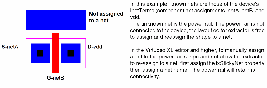
The lxStickyNet property allows a shape to retain the assigned connectivity. In the Virtuoso environment there are two types of nets, known and unknown nets.
-
known nets: nets that are defined by pins and components.
In the Virtuoso XL and higher tier editors, if a shape which is not assigned to a net, touches a shape on known net, the shape is assigned to that net. When the net assignment is defined by pins and components (instTerms), the assignment can not be re-assigned. -
unknown nets: shapes that are not assigned to a net
When a shape touches nothing, it is considered a floating shape.-
When specifying a net name for a floating shape in Virtuoso L, the shape is given the
lxStickyNetproperty and the property is displayed on the property form. -
When specifying a net name for a floating pathSeg created in a route in Virtuoso XL and higher, the route is given the
lxStickyNetproperty and the property is not displayed on the property form. -
The autorouter will assign the
lxStickyNetproperty to routes created as pathSegs created in routes. -
The power router does not create pathSegs in routes, however the shapes will be assign the
lxStickyNetproperty. When a shape is removed from connecting shapes the net name is retained. -
Only one element needs to be marked sticky on a floating island for all the elements to retain the assigned net.
-
When specifying a net name for a floating shape in Virtuoso L, the shape is given the
Support for Voltage-Dependent Rules
Voltage-dependent rules are critical for design processes at 45 nm and less. The support for these rules is based on the ability to use user-defined layer purposes that represent voltage ranges and to define design rule constraint groups within these voltage ranges.
To support these rules, you can define purpose-aware constraints, such as those for width, spacing, and clearance, in the technology file. Purposes are used to propagate the voltage information, though without any connectivity; nets drawn on such purposes are, therefore, called pseudo nets.
The wire editor and the Wire Assistant support the voltage-dependent rules. You can use the voltage-aware, non-drawing layer purposes to create wires, buses, and vias. If you add a via and switch to a higher or a lower layer, the voltage-specific purpose is propagated to the higher or lower layer as you continue the wire or bus creation. The pseudo-net wires you create comply with the voltage-related spacing rules.
You can tap a wire on a voltage-specific layer-purpose pair and create new elements on the same voltage-specific layer-purpose pair.
The following figure shows a section from a sample technology file where the voltage-related purposes are defined along with the parent purposes from which they are derived.
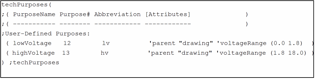
For more information about the techPurposes section of the technology file, see the Virtuoso Technology Data ASCII Files Reference.
The figure below shows these voltage-specific purposes appearing in the Layers assistant:
The section below from the sample technology file sets up a voltage-related constraint group.
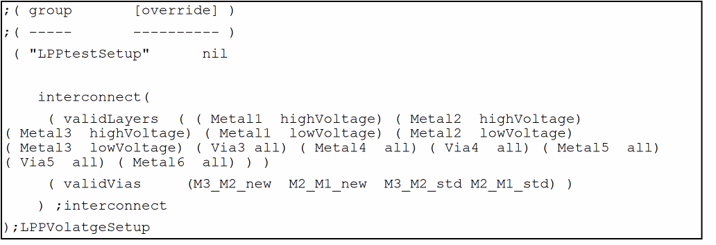
For more information, see the purpose-aware validLayers constraint of the technology file.
From the Seed Attributes From a Constraint Group list on the
The following sections from the sample technology file illustrate the voltage-related rule setups.
For more information, see the
If there are voltage-dependent rules defined in the technology file, the wire editor applies them based on the following precedence, in the order specified:
Layer rule with voltage-dependent purpose > Voltage spacing rule with spacing dependent on the voltage values specified for one layer or two layers > Layer rule with parent purpose > Layer rule
The override value specified in the Create Wire or the Create Bus form takes precedence over the value specified in the technology file if the override value complies with the rule.
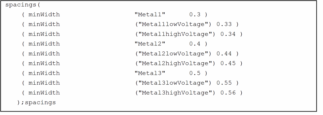
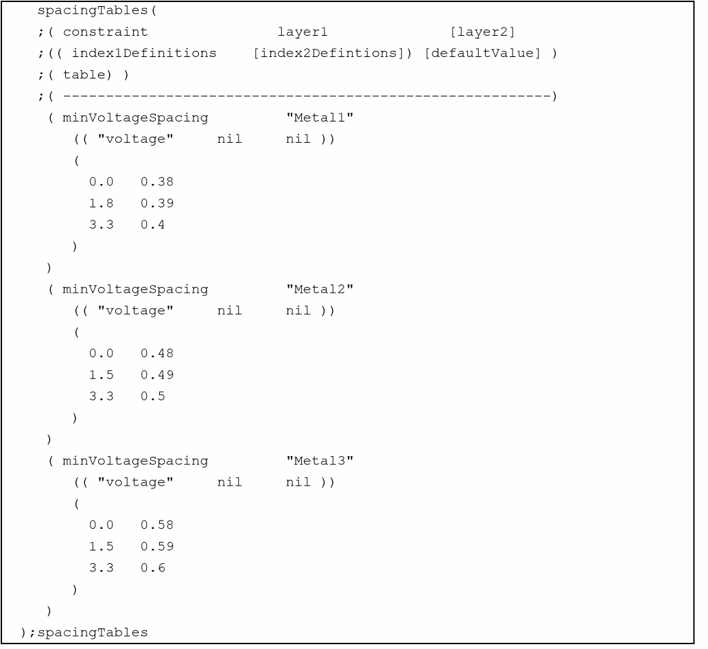
For example, for Metal1, the technology file contains the following spacing rules:
-
minVoltageSpacing -
minSpacing (“Metal1” ” 0.3”) -
minSpacing [(“Metal1” “drawing”) “0.35”] -
minSpacing [(“Metal1” “lv”) “0.33”]andminSpacing [(“Metal1” “hv”) “0.35”]
In addition, the Bit Spacing value (distance between the centerlines of bus wires) specified in the Create Bus form is 0.
In the absence of any override value, the wire editor derives the spacing between the bus wires as per the following lookup precedence:
-
For lowVoltage (lv) layer purpose:
minSpacing (“Metal1” “lv”) > minVoltageSpacing > minSpacing (“Metal1” “drawing”) > minSpacing (“Metal1”) -
For highVoltage (hv) layer purpose:
minSpacing (“Metal1” “hv”) > minVoltageSpacing > minSpacing (“Metal1” “drawing”) > minSpacing (“Metal1”)
Consider a cdsVia device with a Contact Layer purpose, such as open, that does not have a parent purpose defined in the technology file and the purpose is not voltage-related. If you instantiate this cdsVia to change a wire from one layer to another, the purpose of the cdsVia master device is retained. You can verify this by checking the Cut Purpose field in the Edit Via Properties form for the cdsVia. For example, the following cdsVia device is installed in the technology file:
name: M1_M2_Via1layer1 purpose1: Metal1 drawingcutLayer cutPurpose: Via1 openlayer2 purpose2: Metal2 drawing
Create a wire on Metal1 drawing and create the cdsVia M1_M2_Via1 to switch to Metal2 drawing. If you check the properties of the created cdsVia, you will notice the following:
Metal Purpose: drawingCut Purpose: openOther Purpose: drawing
For information about installing and creating cdsVias, see
The interactive and assisted routing commands, such as, Create Bus, Point to Point routing, and Guided routing, use the voltage range information (minVoltage, maxVoltage) on a net to check or enforce Voltage Dependent constraints, such as voltage dependent spacing (minVoltageSpacing). For more information about editing Min Voltage and Max Voltage values, refer to
The voltageSyncNet constraint is also supported for interactive routing commands. Lets see the voltage swing when voltageSyncNet is not defined.
Vswing = Max(Vmax_net1, Vmax_net2)-Min(Vmin_net1, Vmin_net2)
Voltage swing when voltageSyncNet is defined for net1 and net2.
Vswing = Max (abs(Vmax_net1 – Vmax_net2), abs(Vmin_net1 – Vmin_net2))
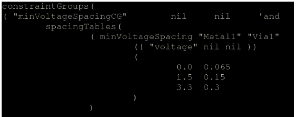
Here is an example with simple values to let you know the difference when voltageSyncNet is defined and when it is not defined.
Lets assume two nets, net1 and net2.
Vmin_net1 = 0, Vmax_net2 = 3.5
Vmin_net2 = 1, Vmax_net2 = 4.5
Voltage swing value when voltageSyncNet constraint is not defined for net1 and net2:
Max(4.5, 3.5)-Min(1.0, 0.0) = 4.5-0.0 = 4.5.
If you lookup the spacing from the table, the minSpacing is 0.3.
Voltage swing value when voltageSyncNet constraint is defined for net1 and net2:
Max(abs(4.5-3.5), abs(0.0-1.0)) = Max(1.0, 1.0) = 1
When you lookup the spacing from the table, the minSpacing is 0.065.
Support for Area-based Rules
You can define different rules for different regions. Once the rules are defined, area-based rules automatically adjust the edited shapes in the design. In interactive routing, area-based rules are disabled by default. To enable area-based rules by default, use the weAreaBasedRulesEnabled environment variable.
The following area-based rules are supported for interactive routing:
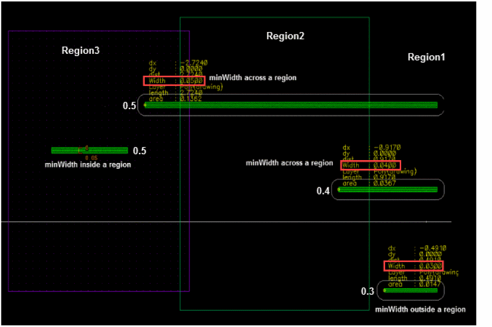
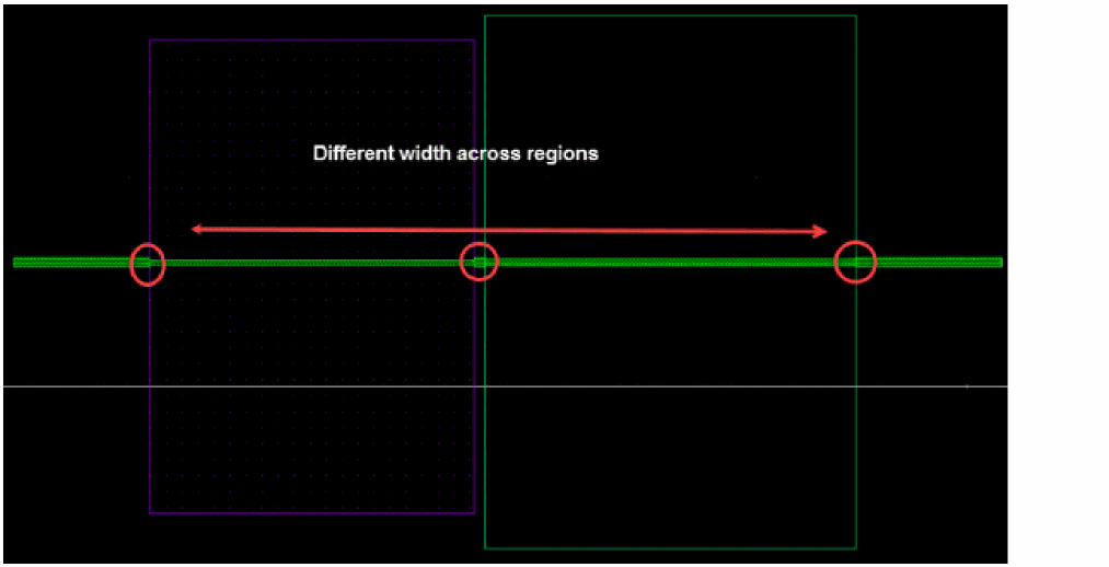
minWidth
When the pathSeg is in a region, it follows the minWidth rule of the region. The minwidth value of a pathSeg that spans regions is the maximum minWidwith value across the spanned regions. For example:
spacings(
( minWidth "Poly" 'vertical 'insideLayers (“DMY1") 0.04 )
( minWidth "Poly" 'vertical 'insideLayers (“DMY2") 0.05 )
( minWidth "Poly" 'vertical 'outsideLayers (“DMY1" “DMY2") 0.03 )
( minWidth "Poly" 'horizontal 0.02 )
) ;spacings
The following figure shows an example of a pathSeg inside a region, outside a region, and across regions. It shows that when the pathSeg spans regions, the maximum minWidth value across the spanned regions is considered.
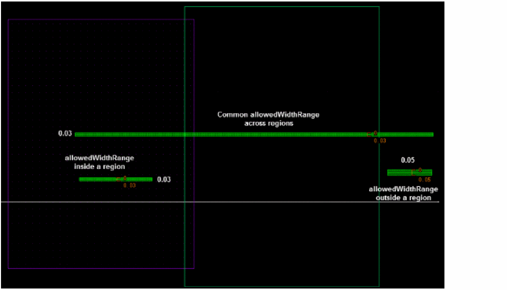
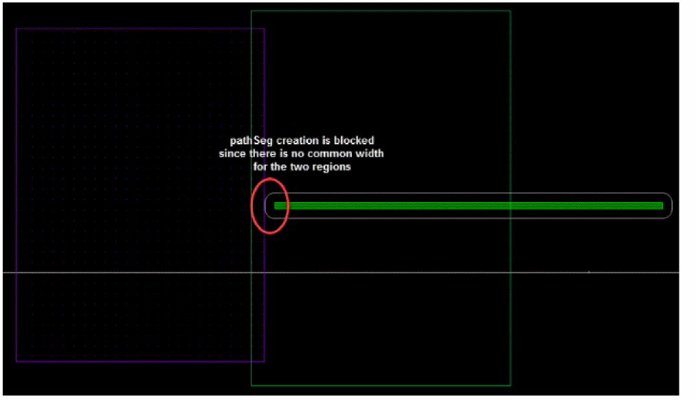
allowedWidthRange
When the pathSeg is in a region, it follows the allowedWidthRange rule of the region. The allowedwidthRange value of a pathSeg uses different widths in different regions when the pathSeg spans across regions.The width value is now controlled by the environment variable.
When the width mode is specified as commonWidth, the width of a pathSeg that spans across regions is the width that is allowed for all the spanned regions. If multiple width values are allowed, the width value nearest to the user-specified width value is used. If there is no common width for the spanned regions, the pathSeg cannot be created across the regions. Here are some examples of the allowedWidthRange area-based rule when the width mode is commonWidth.
spacings(
( allowedWidthRanges "Poly" 'vertical 'insideLayers (“DMY1") (0.03 0.04) )
( allowedWidthRanges "Poly" 'vertical 'insideLayers (“DMY2") (0.03) )
( allowedWidthRanges "Poly" 'vertical 'outsideLayers (“DMY1" “DMY2") (0.03 0.04 0.05) )
( allowedWidthRanges "Poly" 'horizontal (0.03 0.05 ">= 0.08"))
) ;spacings
The following figure shows an example of allowedWidthRange that is specified for a pathSeg when inside a region, outside a region, and across regions. When the pathSeg spans across regions, the common allowedWidthRange of the spanned regions is considered.
spacings(
( allowedWidthRanges "Poly" 'vertical 'insideLayers (“DMY1") (0.03 0.04) )
( allowedWidthRanges "Poly" 'vertical 'insideLayers (“DMY2") (0.06) )
( allowedWidthRanges "Poly" 'vertical 'outsideLayers (“DMY1" “DMY2") (0.03 0.04 0.05) )
( allowedWidthRanges "Poly" 'horizontal (0.03 0.05 ">= 0.08"))
) ;spacings
The following figure shows an example where the pathSeg cannot be created because there is no common width across regions.
However, when the width mode is specified as nonCommonWidth, the pathseg is split when it spans across regions. For each part of the pathseg, the width is adjusted according to the allowed width in each region. Therefore, the pathSeg has different widths for each part and the width for each part is the allowed width that is nearest to the user-specified width, as shown in the following figure.
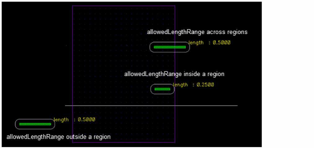
allowedLengthRange
When the pathSeg is in a region, it follows the allowedLengthRange rule of the region. However, when the pathSeg spans across regions, the common allowedLengthRange of the spanned regions is considered. If there is no common length for the spanned regions, the pathSeg cannot be created across the regions.
( allowedLengthRanges "Poly"
(( "width" nil nil ) 'insideLayers ("NWell"))
(
0.01 (">= 0.25")
)
)
( allowedLengthRanges "Poly"
(( "width" nil nil ) 'outsideLayers ("NWell"))
(
0.01 (">= 0.5")
)
)
The following figure shows an example of a pathSeg inside a region, outside a region, and across regions. It shows that when the pathSeg spans regions, the common allowedLengthRange value across the spanned regions is considered.
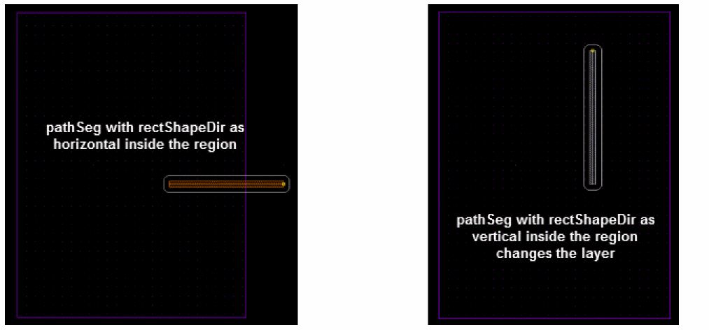
rectShapeDir
When the pathSeg is in a region, it follows the rectShapeDir rule of the region. However, if the direction of the pathSeg in that region is not valid, the layer of the pathSeg is automatically changed to satisfy the rectShapeDir rule.
spacings(
( rectShapeDir “Poly" 'insideLayers (“DMY")
{"horizontal"}
)
) ;spacings
The following figure shows an example, where the rectShapeDir rule defined in the technology file supports the horizontal direction inside the region. As soon as the direction of the pathSeg is changed to vertical, the layer of the pathSeg is automatically changed.
( rectShapeDir “Poly"
(( "width" nil nil ) 'insideLayers (“DMY") )
(
0.03 "vertical"
0.04 "vertical"
0.05 "any"
)
)
When the pathSeg spans across regions, it uses the common width or common direction of the spanned regions. However, if there is no common width or common direction for the spanned regions, the pathSeg cannot be created across regions.
minSpacing
When the pathSeg is in a region, it follows the minSpacing rule of the region. The minSpacing value of a pathSeg that spans regions is the maximum minSpacing value across the spanned regions. For example:
spacings(
( minSpacing "M1" 'insideLayers (“DMY") 0.05 )
( minSpacing "M1" 'outsideLayers ("DMY") 0.1 )
) ;spacings
The following figures show examples of a pathSeg inside a region and across regions. When the pathSeg spans regions, the maximum minSpacing value across the spanned regions is considered.
minSpacing constraints are defined in the technology file of a design, during interactive routing, the constraints are merged and the resultant constraint is used to create a pathSeg. minArea
To support a minArea area-based rule, you must define two constraints in the technology file.
spacings(
( minArea "Metal2" 0.04)
( minArea "Metal2" 'insideLayers ("BuriedNWell") 0.06)
) ;spacings
When a pathSeg is outside a defined global region that does not overlap another region, the minArea constraint of the global region is supported, as shown in the following figure.
When a pathSeg is created inside a region, it follows the minArea rule of that region.
The minArea area-based rule is also supported by Create Bus, Create Stranded Wire, and Stretch commands.
Via Rules
The following via extension area-based rules are supported for interactive routing.
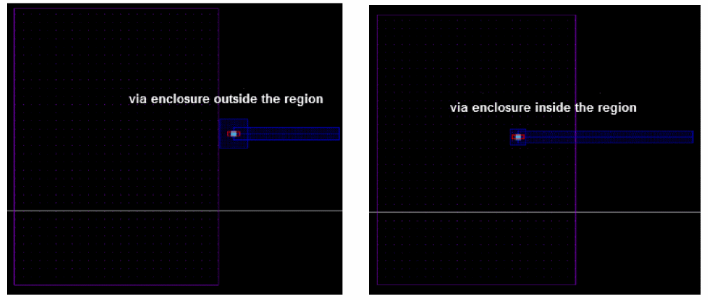
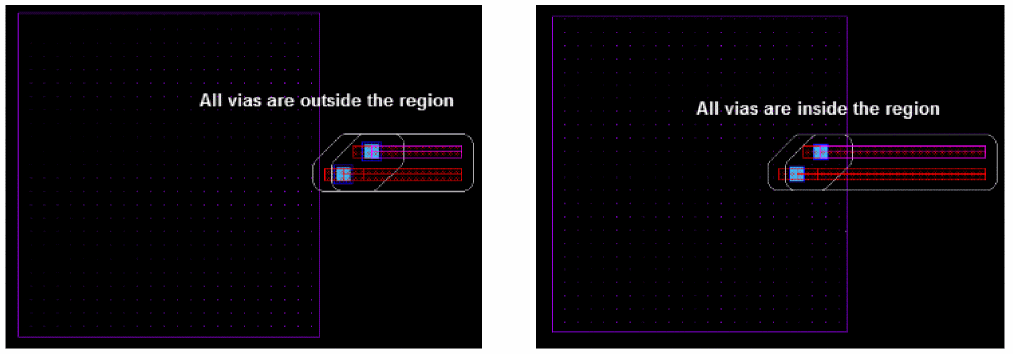
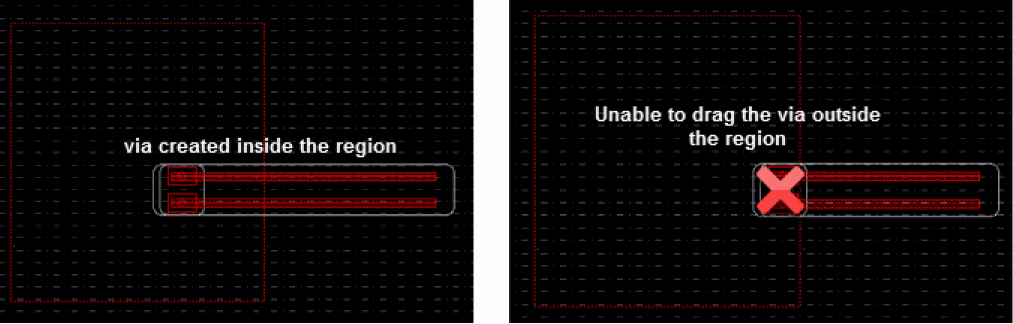
These via rules, when defined in a technology file, apply only to vias that are fully within a region. The enclosure of a via depends on area-based rules defined in the technology file. Also, it is not allowed to have a via partially inside and outside the region.
In addition, if there is more than one via, they must not be in different regions. The via extension is created according to the area-based rule of the region with which the via overlaps.
allowedCutClass
When the allowedCutClass rule is defined for the area inside a region, the area outside the region is considered invalid and vias cannot be added there. Conversely, when the allowedCutClass rule is defined for the area outside a region, the area inside the region is considered invalid and vias cannot be added there. The following figure shows an example when you are unable to add a via outside the region.
In addition, the following figure shows an example when a via is added inside the region and you are unable to move the via outside the region.
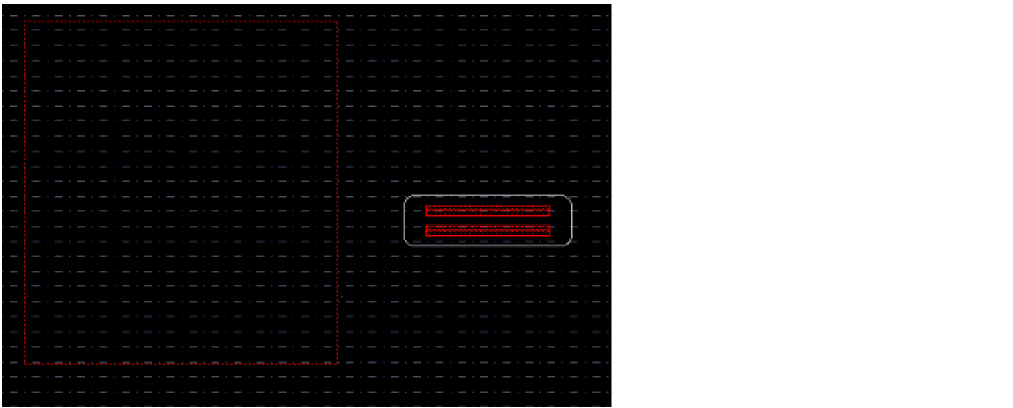
viaKeepoutZone
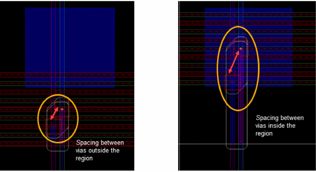
When the viaKeepoutZone rule is defined, the required spacing between vias is different in different regions. The following figure shows an example in the different spacing values when a via is outside and inside a region.
Using Mouse Button Controls
Clicking the right mouse button opens a context-sensitive menu at the point of click. The commands available on the context menu depend on the currently active command.
-
When the Create – Wiring – Wire command is running, clicking the right mouse button opens the Create Stranded Wire Form. You can quickly select the required via, re-adjust the width for wire creation, or fine-tune the wire options.
For information about bindkey controls that appear on the right of various commands on the context menu, see Bindkeys and Access Keys. -
When the Create – Wiring – Wire command is running:
- Pressing the arrow keys allows you to pan across the cellview in four directions.
- Pressing the space bar key places a via or opens the Metal Density Options Form. If only one layer and one via are available for selection, a via is placed and the layer is changed to the only available layer. If the current routing layer has more than one layers available for selection, the Select Via form opens so you can choose a layer or via type.
- When you are creating multiple wires, clicking the right button invokes the Edit Bus Form for bus routing-specific options.
Startup Warnings
Warning or error messages may be issued when invoking a command for the first time due to the loading of data into memory. These messages will appear only once and serve to indicate the issues that have been found with the current data, such as technology file and design constraint discrepancies.
Return to top