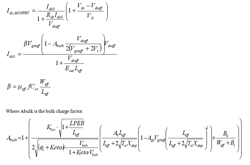
Model Equations
DC current
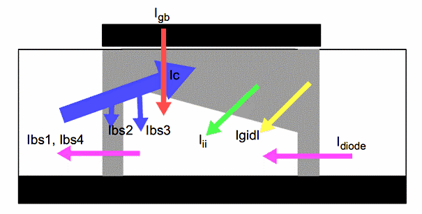
Body current
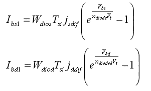
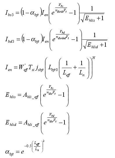
The backward injection current in the B-S/D diode can be expressed as
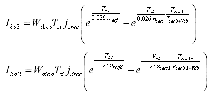
The carrier recombination and trap-assisted tunneling current in the space-charge region is modeled by
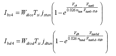
The reverse bias tunneling current, which may be significant in junctions with high doping concentration, can be expressed as
The recombination current in the neutral body can be described by
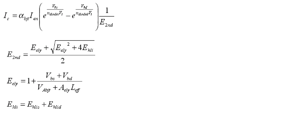
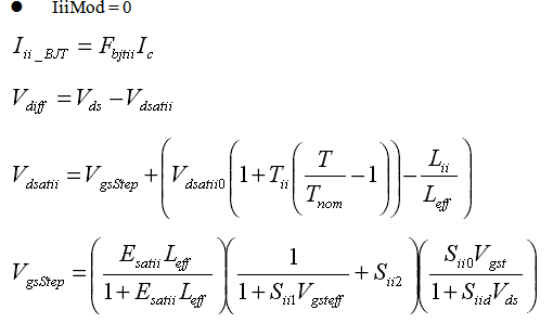
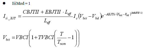
The BJT collector current is modeled as
Impact Ionization Current Equation is modeled as
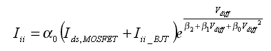
In this expression, the parasitic BJT effect current is modeled as
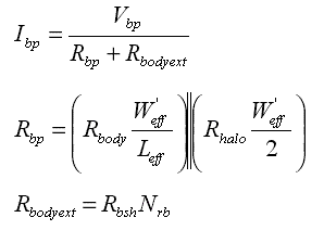
If body contact is applied, there is one more bulk contact current flow into bulk. It is modeled as:
Leakage current
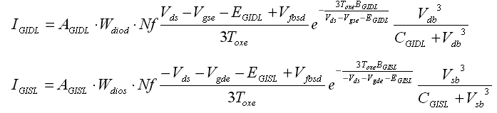
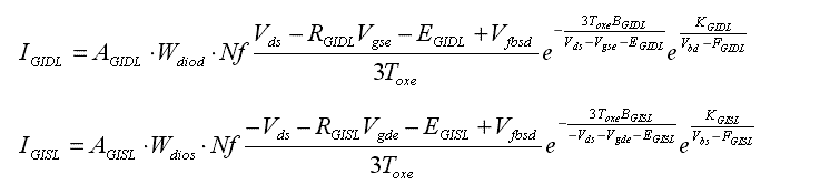
Gate Induced Source/Drain Leakage Current is modeled as:
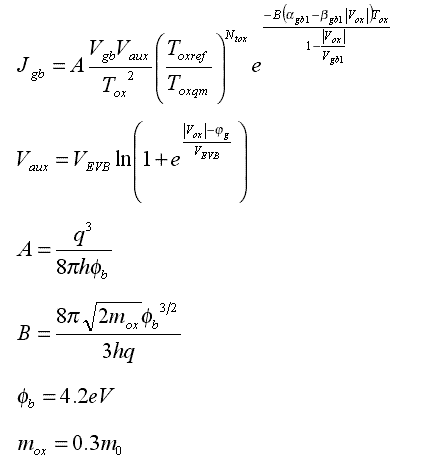
For thin oxide (below 2nm), oxide tunneling is important in the determination of floating-body potential. In inversion, the tunneling current is:
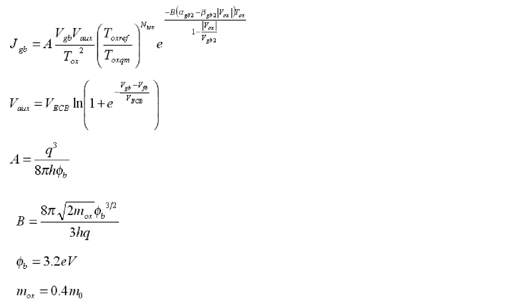
In accumulation, the tunneling current is:
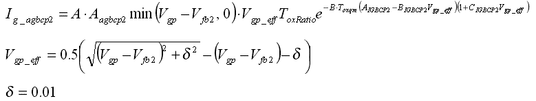
In BSIMSOI4.1, the instance parameter Agbcp2 represents the parasitic gate to body overlap area due to the body contact. This parameter applies for the opposite-type gate. The tunneling current in this region is modeled as:
Charge and Capacitance
The following is the schematic of Charge model in BSIMSOI model.
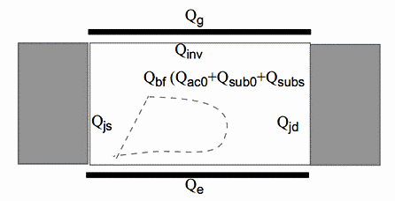
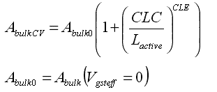
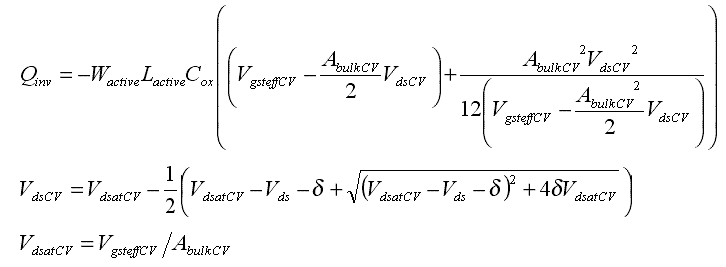
For intrinsic charge, BSIMSOI PD model uses similar expressions to BSIM3v3 for inversion charge (Qinv) and front gate body charge (QBf). The bulk charge constant AbulkCV is defined as:
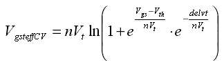
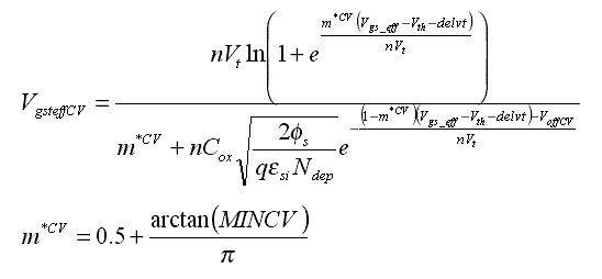
The effective CV Vgst has two equations selected by model parameter vgstcvmod:
The difference between vgstcvmod = 0 and 1 is that vgstcvmod = 1 fixed the bug of vgstcvmod = 0. The default value for vgstcvmod has been changed to 1 from 0 after BSIMSOI model version 4.2.
Then the inversion charge can be expressed as:
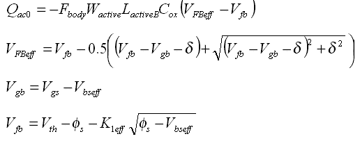
The accumulation charge can be calculated as:
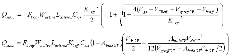
The gate-induced depletion charge and drain-induced depletion charge can be expressed as:
The back gate body charge can be modeled by

For capmod=3, the flat band voltage is calculated from the bias-independent threshold voltage, which is different from capMod=2.
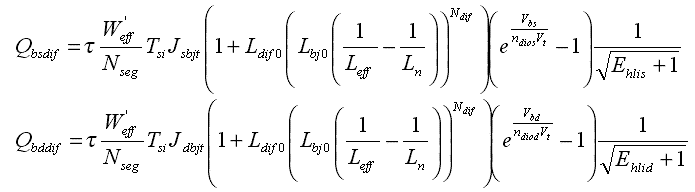
In BSIMSOI PD model, both the depletion and diffusion capacitance of the junction are considered. The diffusion charges Qbddif/Qbsdif are modeled as:
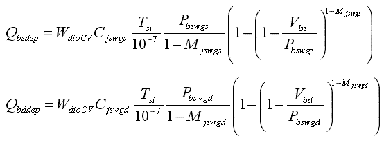
The depletion charges Qbddep/Qbsdep are modeled as:
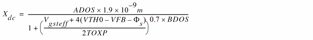
For capmod=3, the inversion charge layer thickness is given by:
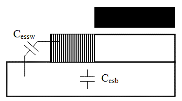
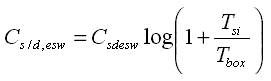
Expressions for source/drain-to-gate overlap capacitance and source/drain-to-gate fringing capacitance are taken from BSIM3v3. New SOI-specific parameters added are substrate-to-source sidewall capacitance (Cesw), substrate-to-drain sidewall capacitance (Cedw), substrate-to-source bottom capacitance (Cesb), and substrate-to-drain bottom capacitance (Cedb). The following figure shows the BSIMSOI extrinsic charge components.
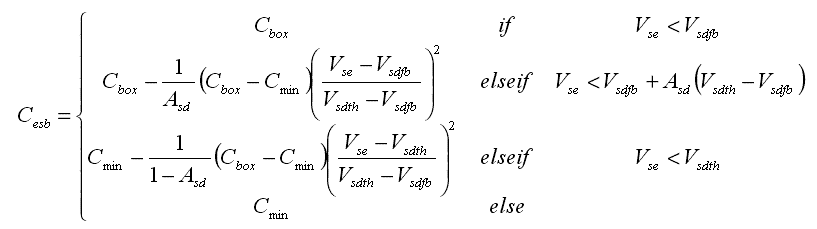
The substrate-to-source bottom capacitance (per unit source/drain area) Cesb is:
The sidewall source/drain to substrate capacitance (per unit source/drain perimeter length) Cs/d,esw is:
Selfheating
An equivalent circuit for self-heating simulation is shown below:
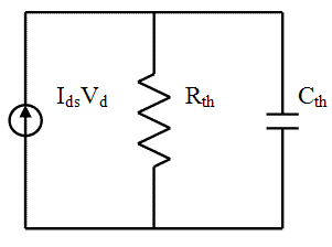
BSIMPD models the self-heating by an auxiliary RthCth circuit shown in the figure above. The temperature node (T node) is created in SPICE simulation if the self-heating selector shMod is on and the thermal resistance is non-zero. The T node is treated as a voltage node and is connected to ground through a thermal resistance Rth and a thermal capacitance Cth.
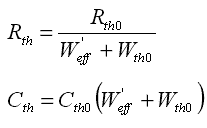
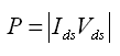
where Rth0 and Cth0 are normalized thermal resistance and capacitance respectively. Wth0 is the minimum width for thermal resistance calculation. The current source is driving a current equal to the power dissipated in the device.
RF model
BSIMSOI provides the gate resistance model used in RF application. You have the following options for modeling gate electrode resistance (bias independent) and intrinsic-input resistance (Rii, bias-dependent):
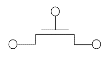
In this case, no gate resistance is generated.
RgateMod=1 (constant-resistance)
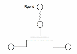
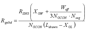
In this case, only electrode gate resistance (bias-independent) is generated by adding an internal gate node. The electrode gate resistance is given by
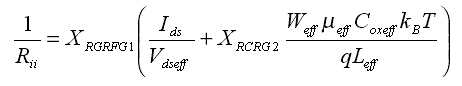
RgateMod=2 (RII model with variable resistance)
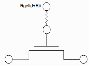
The gate resistance here is the sum of the electrode resistance and the intrinsic-input resistance Rii, as given by:
RgateMod=3 (RII model with two nodes)
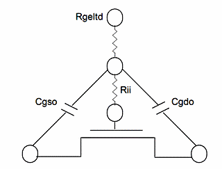
The gate electrode resistance here is in series with the intrinsic-input resistance Rii through the two internal gate nodes so the overlap capacitance current does not pass through the intrinsic-input resistance.
Noise
In BSIMSOI model, flicker noise and thermal noise models are compatible with BSIM4. Gate tunneling induced shot noise and thermal noise due to gate electrode resistance are also included.
Two flicker noise models are provided in BSIMSOI model:
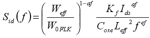
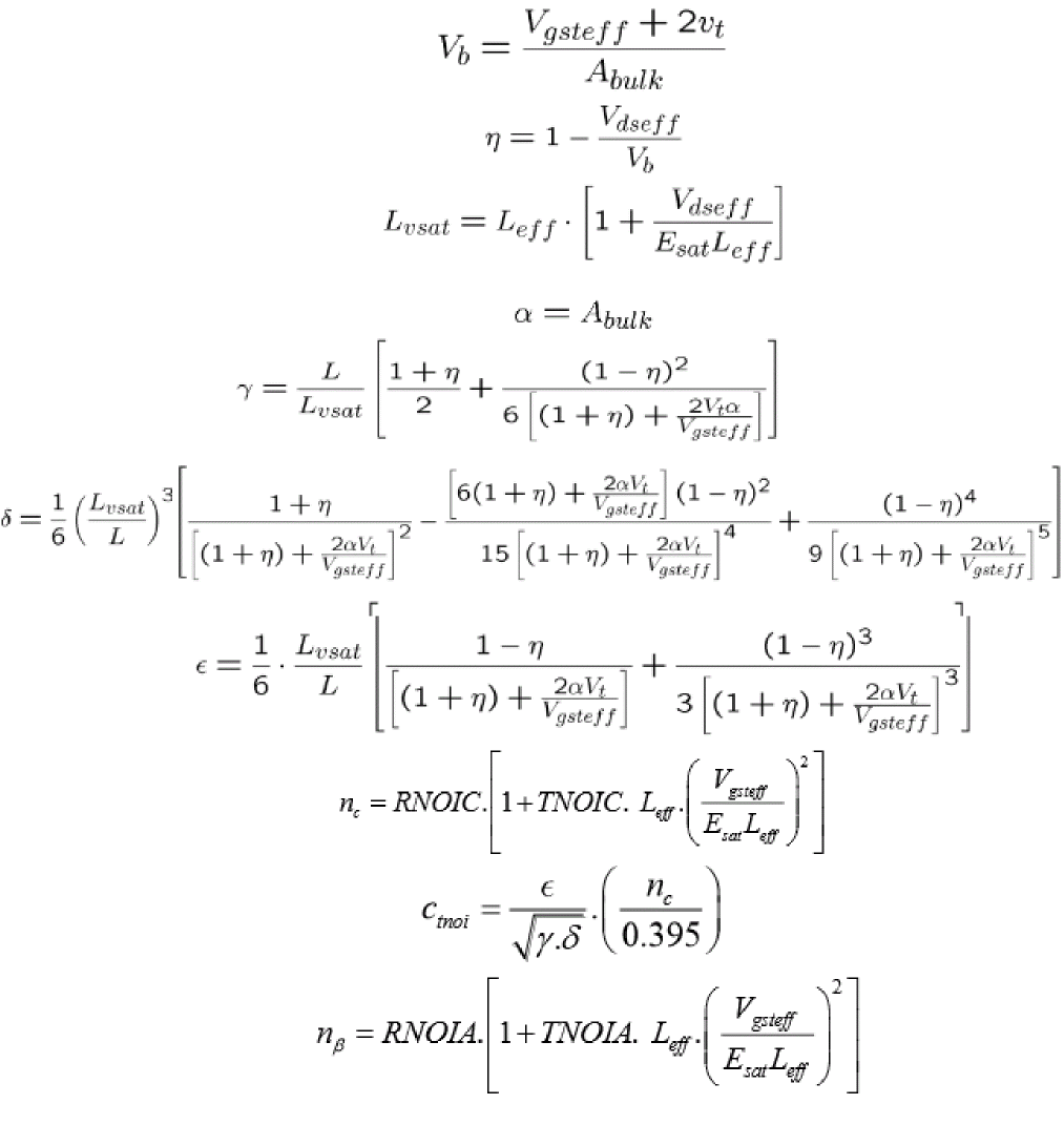
The noise density in inversion region is given by:
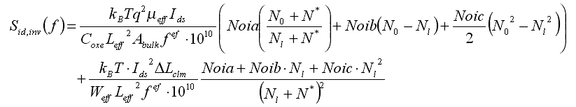
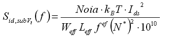
The noise density in subthreshold region is given by:
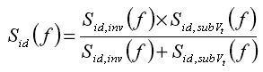
The total flicker noise density is:
Following thermal noise models are provided in BSIMSOI model:
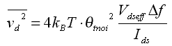
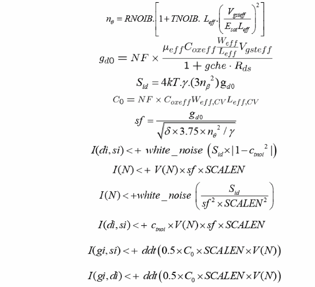
The noise voltage source partitioned to the source side is given by:
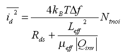
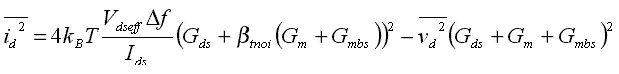
The noise current source put in the channel region with gate and body amplification is given by:
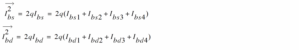
The junction currents ( Ibs, Ibd) for shot noise(fb_ibs, fb_ibd) are given by:

The NTNOI parameter provides the flexibility to tune the magnitude of noise density.
In this noise model, noise for both gate and drain is implemented as current noise sources. The drain current noise flows from drain to source, whereas the induced gate current noise flows from gate to source and drain. The correlatoin between the two noise sources can be tuned with the parameter RNOIC.
Related Topics
BSIMSOI MOSFET Model (bsimsoi)
Return to top