1
Introduction
The Virtuoso® Custom Digital Placer automatically places transistors, devices, and cells in block and cell designs.
The Custom Digital Placer is a generic placer that can be used for placement in different types of designs such as designs that contain only standard cells, designs that contain only devices, or designs that contain both standard cells and devices. You can also use the placer for generating connectivity and constraint-driven placement.
However, before you can use the placer to automatically place devices, you must generate the layout connectivity and circuit components by using Layout XL editor. The placer uses the schematic design as the connectivity source for placing the components.
This chapter covers the following topics:
- Key Features
- The Placement Commands
- Placement Types
- Placement Of Different Component Types
- The Placement Flow
- Setting Up Layout XL for Placement
- Setting Placement Constraints
- Defining Component Types and Placement Parameters
- Troubleshooting Placement
Key Features
- Connectivity and constraint-driven placement to achieve overall shortest wire length.
- Placement of designs that contain:
- Support for the following placement types:
- Support for incremental and selective placement.
- Support for the following placement constraints
- Support for the following routing constraint
-
Automatic row generation for both standard cell and device-level MOS and FinFET designs
- Automated pin placement user interface that lets you:
The following sections contain more information about using the Custom Digital placer.
- Setting Up Layout XL for Placement
- Setting Placement Constraints
- Defining Component Types and Placement Parameters
- Troubleshooting Placement
For information about the placer forms, see Custom Digital Placer Forms.
The Placement Commands
In Layout XL, the placement commands supported by the Virtuoso Custom Digital Placer are available under the Place menu. These commands are:
-
Custom Digital – Placement Planning: Use this command to open the Placement Planning form for creating, modifying, and deleting rows for placing the design components.
-
Custom Digital – Placer: Use this command to run the automatic placer for performing placement.
 , on the Custom Digital Placer toolbar.
 , on the Custom Digital Placer toolbar.
In addition to the placement commands listed above, the Place menu supports the following commands that can be used for placement:
- Pin Placement: Use this command to specify the pin location constraints and to preplace pins, independent of the main placement run.
- Update Placement Status: Use this command to update the placement status of instances or pins that are loaded in Layout XL for the first time, or which have been edited outside the Layout environment.
Other Commands Used with the Placer
-
Edit – Component Types opens the Configure Physical Hierarchy window in the Component Types mode. Use this window to update your library with information that guides the placement of components in rows, and to define parameters for MOS device chaining and folding.(Virtuoso Advanced Node for Layout Standard) The Configure Physical Hierarchy window can also be used to define parameters for FinFET chaining and folding.For more information, see Component Types in the Virtuoso Layout Suite XL User Guide.
-
Create – P&R Objects – Row opens the Create Row form. Use this form to create rows for placement.
For more information about the method for creating rows manually, see Creating Rows in the Virtuoso Layout Suite documentation. -
Create – P&R Objects – Custom Placement Area opens the Create Custom Placement Area form. Use this form to create a custom area for placement.
For more information about the method for creating a custom placement area, see Creating a Custom Placement Area in the Virtuoso Layout Suite documentation. - Create – P&R Objects – Clusters opens the Create and Edit Clusters form. Use this form to specify the components that must be grouped together during placement.
-
Create – P&R Objects – Cluster Boundary opens the Create Cluster Boundary form. Use this form to define a boundary to enclose one or more clusters. You can then specify the cluster boundary you want to place during placement planning.
For more information on creating clusters and cluster boundaries, see Creating Clusters.To modify the existing component type assignments and to update the default component alignment and orientation before the components are placed, use the Dressing Template Editor form. You can open this form by clicking the Dressing Template Editor button on the Create Row, Create Custom Placement Area, or the Placement Planning form.
Placement Types
The Custom Digital Placer supports the following placement types:
Row-based placement
Row-based placement is a structured placement type that lets you place specific component types within rows. This placement type is most suited for placing standard cells and devices that have at least one “standard” dimension. For this reason, row-based placement is considered most suitable for designs that contain only standard cells.
In addition to providing a structured placement, row-based placement lets you constrain the components within a row to specific orientations and alignments. Given the uniform and structured placement it helps to obtain, row-based placement is considered a more economical and optimal placement type.
You can choose from the following modes for defining rows:
- User-defined (manual) mode: Use this mode to manually define the geometry of a series of rows and the components within. Using this placement mode, you can specify not only the number of rows to be placed but also define their location on the canvas and the alignment and orientation of the components to be placed within these rows.
- Component-assisted mode: Use this mode to automatically determine the row geometries based on the specified area utilization goals and other design goals. Using this placement mode, you can manipulate various design factors to explore different placement outcomes.
Area-based placement
Area-based placement is less restrictive of the two placement types supported by the Custom Digital Placer.
This placement type places the components anywhere within the available placement boundary, unless the components are locked outside the boundary. Area-based placement does not require component types or constraints to be defined. However, if any individual constraints are placed on the components, they are honored.
If individual constraints on components or groups of components do not exist, the placer only targets to reduce the overall wire length and achieve a balanced placement. Therefore, in the absence of constraints, the components tend to spread out using all the area allowed for placement.
Placement Of Different Component Types
You can use the Custom Digital Placer to place designs that have only standard cells, only devices, or a combination of both, standard cells and devices.
Standard (or custom) cells are placed in horizontal or vertical rows. Depending on their number, the placer can place all the cells within a single row or across multiple rows.
For more information about placing components within rows, see Row-based placement.
Devices follow a row-based MOS, transistor-level placement.
Since MOS devices support diffusion-sharing to enable chaining, you can automatically or interactively chain devices at the time of layout generation to optimize placement. Such placement maximizes the diffusion sharing to minimize the diffusion gaps in the generated layout.
For designs with a mix of component types, such as PMOS, NMOS, STDCELL, STDSUBCONT, and FILLER, depending on the cell type, both row-based and MOS transistor-level placement is followed.
Placing NFIN and PFIN Components (Virtuoso Advanced Node for Layout Standard)
The Custom Digital Placer can be used for placing NFIN and PFIN component types.
Global Snap Pattern Grid Support
VCP has been enhanced to support snap patter pattern (SP) / width spacing snap pattern (WSP) grid definitions:
-
The Snap Pattern (SP) grid defined using the
snapPatternDefrule in the technology file.
For detailed information aboutsnapPatternDef, see Snap Pattern Definition Requirements in the “Technology File Requirements for FinFET-based Design” chapter of the Virtuoso FinFET Support Overview manual. -
The Width Spacing Snap Pattern (WSP) grid defined using the
widthSpacingSnapPatternDefrule in the technology file.
For definition of thewidthSpacingSnapPatternDefrule and related technology file information, see Width Spacing Patterns.
To support snapping of devices and standard cells to the required snap pattern grid, VCP has undergone the following key enhancements:
-
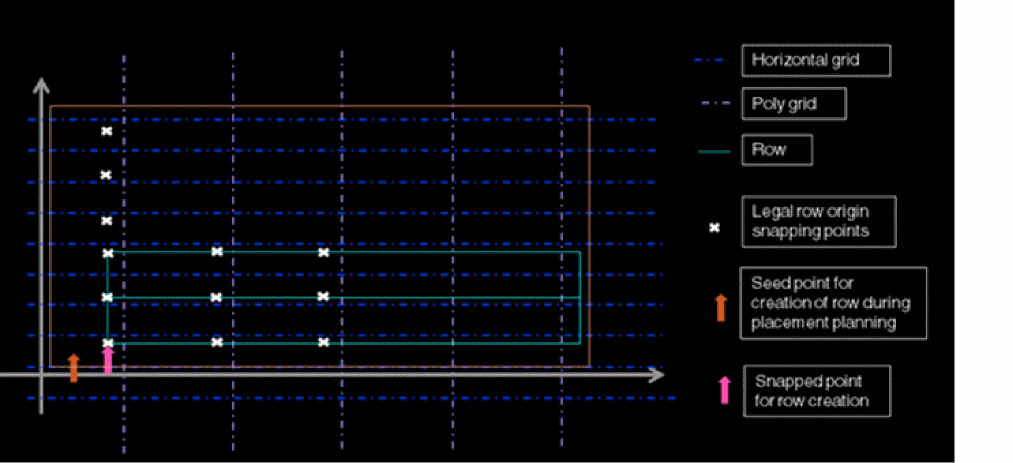
Row creation follows pattern-aware snapping.
Row creation is based on reference grids and their respective offsets selected by the user at the time of Placement Planning. Ref X Grid and Ref Y Grid in the Placement Planning form specify the reference grids for snapping devices and rows. Ref X Offset and Ref Y Offset are the offsets applied to rows after they are snapped to the Ref X Grid and Ref Y Grid. If the Ref Y Grid is set to NONE, which is the default behavior, then the rows are snapped to thesiteDefswidth defined in the technology file.
For more information, see Planning a Placement. -
Auto Placer follows pattern-aware snapping.
Auto Placer now honors the local/global snap pattern definitions in the technology file or in the design. During placement, devices are automatically snapped to the snap pattern grid.
Here is an illustration representing how the seed point for row creation during placement planning is different from the point of row creation, which is snapped to the grid specified in the Placement Planning form.
The Placement Flow
The placement flow for row-based designs typically involves the following steps:
-
Define component types using the Component Type mode of Configure Physical Hierarchy to assign the devices to rows and set the parameters for device chaining and folding.
See Component Types in the Virtuoso Layout Suite XL User Guide. -
(Optional) Generate layout representations for critical components by using the Layout XL Connectivity - Generate - Selected From Source command.
See Generating Selected components from Source in the Virtuoso Layout Suite XL User Guide. -
Generate a layout and a preliminary placement for the remaining design components by using the Connectivity - Generate - All From Source command or the Connectivity - Update - Components and Nets command.
See Generating All Components from Source and Updating Components And Nets in the Virtuoso Layout Suite XL User Guide. -
(Optional) Place and constrain pins by using the Place – Pin Placement command.
See Pin Planning. - Create rows for placing the components, specify the component types to be placed in them, align the components to the respective rows, and specify the component orientation by using the Placement Planning command.
-
(Optional) Set the appropriate placement constraints.
See Pin Placement Constraints. -
(Optional) Set the Net Priority routing constraint for assigning higher priority to critical nets.
See Net Priority in the Virtuoso Custom Constraints User Guide. -
Run the automatic placer by using the Place – Custom Digital – Placer command to automatically position the unplaced design components on the layout canvas.
See Running the Placer. - Examine the placement. If required, update the constraints you set and run the placer again.
Setting Up Layout XL for Placement
This section describes some Layout XL environment variables you might want to set and some design-related decisions you should make before you begin working with the placer.
- Setting the Netlisting Mode
- Defining the Placement Region
- Abutting Standard Cells
- Setting MOS Chaining and Folding Parameters
- Using Automatic Abutment During Placement
Setting the Netlisting Mode
To enable the placer to correctly handle permutable pins, ensure that the CDF parameters are evaluated correctly by setting the CDS_Netlisting_Mode shell environment variable to Analog or Compatibility.
To set the CDS_Netlisting_Mode environment variable for the current session,
-
Type the following commands in the CIW.
setShellEnvVar("CDS_Netlisting_Mode=Analog")

cdsSetNetlistMode()
To check the mode in which the environment variable is currently set:
CDS_Netlisting_Mode to Digital.
For more information about the CDS_Netlisting_Mode, see
Defining the Placement Region
The prBoundary object representing the place and route boundary defines the available placement region.The prBoundary can be a single rectangle or a polygon.
Abutting Standard Cells
By default, all standard cells—cells defined with component type STDCELL—are designed to support abutment. This implies that all standard cells abut together without creating design violations. Therefore, when placing abutted standard cells, the placer only checks the design rules between the boundaries of the adjacent standard cells. Rules between the internal objects in a standard cell are not validated.
In other words, the placer considers the boundary of each standard cell as its abutment edge. This ensures that the placement is optimal.
STDCELL—and devices belonging to other component classes.The placer determines the cell boundary for each standard cell by using the following precedence:
- The list of layer-purpose pairs defined in the vcpCellBoundaryLPPs environment variable.
-
The (
prboundarydrawing) layer-purpose pair. -
The (
prboundaryboundary) layer-purpose pair. -
The (
instancedrawing) layer-purpose pair.
If none of the above layer-purpose pairs exists in the cell, a boundary is derived equal in size to the sum of the objects within the cell.
To ensure that the objects within adjacent standard cells can be shared or overlapped during placement without generating any abutment violations, the cell boundary must be defined by using the vcpCellBoundaryLPPs environment variable.
Setting MOS Chaining and Folding Parameters
To place the MOS devices optimally, you must set the following .cdsenv environment variables to chain and fold them before placement.
Using Automatic Abutment During Placement
If switched on in Layout XL, automatic abutment is performed during layout generation for assisted MOS devices. To use automatic abutment:
- Select the Abut transistors option on the Connectivity form.
-
Set the appropriate abutment properties on your design components including those on MOS device parameterized cells.
See Setting Up Pcells for Abutment in the Virtuoso Layout Suite XL User Guide.
For an example of a MOS device parameterized cell, see thespcnmosandspcpmosdevices in the sample parameterized cells library. For more information, see the Sample Parameterized Cells Installation and Reference.
Setting Placement Constraints
To constrain the placement of devices or pins in your design, you can directly set geometric or pin placement constraints using the Constraint Manager or using an associated SKILL Function.
-
Geometric Constraints are used to control the placement of objects. You can create them using the Constraint Manager assistant or by using an associated SKILL function.
- For information about the types of constraints and how they are supported by the custom digital placer, see Geometric Constraints.
- For information about creating constraints through the Constraint Manager assistant, see the Virtuoso Unified Custom Constraints User Guide.
- For information about creating geometric constraints using a SKILL function, see the Virtuoso Layout Suite SKILL Reference.
-
Pin Placement Constraints are used to control the placement of pins. You can create them using the Pin Placement form. The form lets you place different types of constraints on multiple pins at one time and automatically moves the pins to their assigned locations.Alternatively, you can create pin placement constraints using the Constraint Manager or by using an associated SKILL function.For more information, see Pin Placement Constraints.
Geometric Constraints
You can create the following constraints in the Constraint Manager assistant for placement of objects:
- Alignment Constraints
- Cluster Constraints
- Distance Constraints
- Fixed Constraints
- Symmetry Constraints
Alignment Constraints
The placer supports alignment references on any layer or on the instance bounding box. The first object selected is considered as the alignment reference object and the remaining objects selected are aligned to that reference.
The Custom Digital Placer supports the following Alignment Constraint options:
For more information about the Alignment constraint, see
Cluster Constraints
The placer honors non-hierarchical cluster constraints that are set to specify the logical association among the instances within a cellview. Each cluster is associated with one or more rectilinear cluster boundaries within which the instances associated with that cluster are placed.
Depending on the members it accepts, a cluster can be:
- inclusive - Instances other than the instances in this cluster can be placed within its associated cluster boundaries. However, the instances that belong to this cluster cannot be placed outside of its associated boundaries.
- suggested - Instances can be placed inside or outside the associated cluster boundaries.
- exclusive - Only those instances that belong to this cluster can be placed within its associated cluster boundaries.
- The cluster boundary associated with a cluster of type “inclusive” or “suggested” is considered to be a soft fence for the cluster.
- The cluster boundary associated with a cluster of type “exclusive” is considered to be a hard fence for the cluster.
To define a cluster constraint on a selected set of components, run the Cluster command from the Placement constraints available in the Constraint Manager. To define a boundary for the cluster, select the Create – P&R Objects – Cluster Boundary command. To set the type of a cluster, choose a value for the Type field in the right panel on the Create and Edit Clusters form. To open the form, select the Create – P&R Objects – Clusters command.
For more information about the Alignment constraint, see
Distance Constraints
The placer honors the distance constraint between two or more devices. However, when setting constraints for multiple devices, you must define the acceptable distance parameters between each pair of devices for the placer to interpret them.
You can constrain the devices in one direction—X or Y—but not in both directions simultaneously. However, after the devices have been constrained, the placer aligns them in the orthogonal direction.
The Custom Digital Placer honors the following Distance Constraint attributes:
For more information about the Distance constraint, see
Fixed Constraints
The placer honors the fixed constraint that is set to limit the position of one or more components with an allowable set of orientations to a particular x and y location.
The Custom Digital Placer supports the following Fixed Constraint options:
For more information about the Fixed constraint, see
Symmetry Constraints
The placer interprets the order between the device pairs involved in a symmetry constraint. For example, if Q1 and Q2 are constrained along their horizontal line, then the constraint implies that Q1 lies below the horizontal line and Q2 lies above it. If the devices are constrained along a vertical line, based on the symmetry constraint, Q1 should lie to the left of the vertical line and Q2 to the right.
The placer supports the following types of symmetries:
The Virtuoso Custom Digital Placer supports the following Symmetry Constraint options:
For more information about the Symmetry constraint, see
VCP honors the database cell symmetry set as an OA cell property on the cell master to derive allowed orientations as per the following table:
Pin Placement Constraints
There are three ways in which you can set placement constraints on pins. These are:
Setting Pin Placement Constraints using the Constraint Manager Assistant
You can set distance, alignment, grouping, symmetry, and fixed pin constraints by using the Constraint Manager assistant. For information about these constraints and how they are supported by Layout XL and the placer, see Geometric Constraints.
Depending on the requirement of your design, you can set multiple constraints using the Constraint Manager. For example, if you want to constrain pins to an edge of a bounding box with a specified pitch, you must create an alignment constraint and a distance constraint.
For more information about setting constraints through the Constraint Manager assistant, see the Virtuoso Unified Custom Constraints User Guide.
Setting Pin Placement Constraints using the Pin Placement Form
The advantage of using the Pin Planner form is that it lets you set and apply multiple constraints on multiple pins simultaneously. After you click Apply, the specified pins are automatically moved to the specified positions.
You can set the following constraints using the Pin Placement form.
The Pin Placement form lets you assign pins to a fixed location or to a particular edge and order them along each edge according to your requirement. You can also specify fixed spacing for a group of pins that you have ordered and aligned to a particular edge.
For example, you have a polygon with six edges and you want to place three pins (pin1, pin2, and pin3) on edge number 5. When you specify this in the pin placer form, it creates an alignment constraint as follows.
For more information about setting constraints through the Pin Placement form, see the Pin Planner form.
Setting Pin Placement Constraints using SKILL Functions
You can set placement constraints on pins by using SKILL Functions.
Defining Component Types and Placement Parameters
The information about the “type” of each design component is required to specify the chaining and folding parameters for the components, and to define how the various component types are assigned to rows.
Currently, there is no need to define the component types for placing the components by area. In other words, if the component types are not specified, the components are placed by area.
You can define component types by using the Edit – Component Types command.
Depending on the requirement of your design, you can define the component types at the library level or at the individual cell level.
Irrespective of their type, the components are placed within the place and route boundary unless:
- The devices have been locked or fixed to a particular location outside the place and route boundary.
- The Place Selected Only option in the Auto Placer form is selected.
- If the placer does not place a component in a row, use Edit – Component Types to verify that the component in question has been correctly assigned to an appropriate component type, and that the row definition allows for that particular component type to be placed.
- If some components in the design are not assigned a component type, the placer ignores these components when calculating the required rows and subsequently ignores them during placement.
Defining a Standard Cell Substrate Contact
Standard cell substrate contacts, also called tap cells, are physical-only filler cells that are inserted between devices to limit resistance and to establish connection between the VDD and GND rails, thereby preventing DRC errors and latchup effects.
Standard cell substrate contacts are neither contacts nor vias; they are standard cells assigned to component types with the component class STDSUBCONT.
Standard cell substrate contact insertion is done on a per-row basis. Therefore, the location of standard cell substrate contacts in each row is independent of the placement of standard cell substrate contacts in other rows.
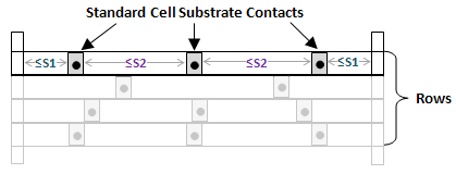
In the above diagram, S1 represents the offset of the first and last substrates from the respective row edges, and S2 represents the distance between two consecutive substrates.
You can specify the maximum and minimum spacing values between two consecutive substrates by using one of the following methods:
- Using the Use Substrate Contacts field in the Placement Planning form
- Defining the Substrate Contact Spacing Properties
The values for S1 range from 0 to half of the value of S2. For example, if you specify 1 and 4 as the minimum and maximum values for S2, the value of S1 can range from 0 to 2. The Auto Placer respects these values during placement.
Use the Swap Tap Cells feature to detect tap cells with maximum spacing violations. You can also replace them with tap cells that have valid maximum spacing values.
For more information about this feature, see Swapping Tap Cells.
Defining the Substrate Contact Spacing Properties
To add standard cell substrate contacts, you need to define the following properties:
-
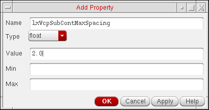
lxVcpSubContMaxSpacing, which specifies the maximum spacing after which the placer must place another standard cell substrate contact in order to avoid a violation. Specify this property on the layout master for the substrate contact. -
lxVcpSubContMinSpacing, which specifies the minimum spacing allowed between two adjacent standard cell substrate contacts. Specify this property on the layout master for the substrate contact.
- Copy an existing filler cell, which is to be used as the basis for the standard cell substrate contact.
-
Add substrate and well contacts to the cell. You can use
oaVia, via instance, or polygons to do this. -
Add the
lxVcpSubContMaxSpacingandlxVcpSubContMinSpacingproperties to the cellview.
For example, to setlxVcpSubContMaxSpacing, do the following.-
From the layout window, choose Edit – Basic – Properties – Cellview.
The Edit Cellview Properties form appears. - Click the Add button to display the Add Property form.
-
Specify the property parameters, as indicated in the figure below, and click OK to set the property.
-
Repeat steps a through c to add the
lxVcpSubContMinSpacingproperty. - Click OK to set the properties and close the Edit Cellview Properties form.
-
From the layout window, choose Edit – Basic – Properties – Cellview.
- Choose Edit – Component Types to display the Configure Physical Hierarchy window in the Component Types mode.
- Assign a component type to the new cell that you created, which has its Component Class set to STDSUBCONT. (Create a new component type, if required.)
-
(Optional) Specify the view name to be used for placing the cells of class STDSUBCONT.If the view name is not defined, the placer traverses through the Physical stop view list in the Global Bindings section of the Configure Physical Hierarchy form to determine the view type to be used.
-
Run the automatic placer after selecting the Insert Standard Cell Substrate Contacts option selected.
The placer fills any gaps between the placed cells with the specified standard cell substrate contacts.
Placing Standard Cell Substrate Contacts in Alternate Rows
By default, substrate contacts (tap cells) get placed in consecutive rows. But, if required, you can force them to be placed in alternate rows. However, for this to be supported by the placer, the rows in which the substrate contacts are to be placed must be created in flipped and abutted manner. This means the rail pattern should be PGGP or GPPG and the row-to-row spacing must be zero.
To place substrate contacts in alternate rows:
-
In the Placement Planning form, select In Alternate Rows option on the Component tab.
Alternatively, set the subContInAlternateRow environment variable.
With substrate contact placement in alternate rows selected, the placer places the substrate contacts in alternate rows, such as the 1st, 3rd, 5th, and so on. But, if the total number of rows created is even, the substrate contacts will also be placed in the top row. For example, if the total number of rows generated is 6, the substrate contacts are placed in the 1st, 3rd, 5th, and the 6th rows.
MOS Transistor Chaining and Folding Parameters
After the devices are assigned a component type, the MOS transistors that need to be chained and folded must have certain parameter values set before you generate a layout.
Troubleshooting Placement
This section discusses common placement problems and some possible solutions.
Room Violations
Room violations are spacing violations that occur when the components placed within a partition are overlapped by another partition or when two partitions overlap.
By default, the VCP engine excludes components that do not belong to the partition to be placed. However, room violations might still be observed if the partition itself is overlapped by another partition.
The markers generated due to room violations in a design are displayed in the
To fix room violations, manually move around the overlapping shapes.
Return to top