- Overview
- Technology and IP Library Preparation
- Verilog Netlist Creation
- General comments
- Floorplanning
- Floorplanning of Verilog Netlist Using Blackboxes
- Generate From Source for Soft Analog Block Layout Using Virtuoso
- Load Physical View to Merge Optimized Pin Locations and Block Boundary
- Physical Implementation of Soft Analog Blocks Using Virtuoso
- Physical Implementation of Soft Digital Blocks Using Innovus
- Top-level Analog Net and Power Routing
- Top-level Design Implementation
- Final Chip Integration and Sign-Off
- ECO Flows
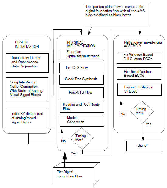
8.1 Overview
Most of the designs today are mixed signal in nature. A typical SoC may look like a pool of analog mixed signal IPs with a lot of embedded mixed signal logic into it. To enable mixed signal floorplanning, advanced interactive and automatic editing and pre-routing, chip assembly capabilities within the Innovus layout environment, Cadence has provided concurrent floorplanning flow using Virtuoso and Innovus. This allows you to plan, implement and connect blocks within a physical layout environment, eliminating the need for time-consuming and error-prone data abstractions and conversions.
A typical netlist-driven mixed signal flow may look similar to the digital implementation flow with minor differences during floorplanning, top level specialty net routing, and ECO flows.
8.2 Technology and IP Library Preparation
- During this stage, you are expected to merge the technology LEF data into its base PDK using the details provided in the Technology Data Preparation chapter. The chapter also describes the dos and don'ts that you need to observe to achieve smooth interoperability of design data between Virtuoso and Innovus platform.
- Design library creation requires special care so that all the technology tree is visible to both the tools with proper reference and/or attach mechanism of design library preparation.
- All the cells used in the design are provided to Innovus in the form of reference OpenAccess libraries instead of the standard LEF files.
- Some environment settings need to be used before the start of Innovus and/or Virtuoso session. These are described in the Useful Tips chapter.
8.3 Verilog Netlist Creation
The Verilog netlist for the netlist-driven mixed signal flow is generally created through Synthesis. In this flow, the analog block is treated as a hard block during synthesis.
8.4 General comments
- Just as for any other design in Innovus, you need to prepare the timing and power intent definition files for more accurate and elaborate analysis within Innovus. Defining power intent through CPF is the recommended methodology.
- Quick abstract inference can be use for fast changing blocks containing digital and analog. This eliminates the need to generate abstract views again and again. Innovus requires an abstract view for all blocks in the design. As custom blocks may only have a layout view during the implementation phase, this capability is useful for creating the required abstract automatically during the floorplanning phase of the design.
- Static timing sign-off is fast becoming a requirement for mixed signal designs, which have timing paths between the digital and analog circuitry. Cadence offers an approach using a full timing model for mixed signal blocks, so exhaustive characterization of such blocks is not necessary.
8.5 Floorplanning
Netlist-driven mixed signal floorplanning flow can be divided into four stages depending on the maturity of the netlist.
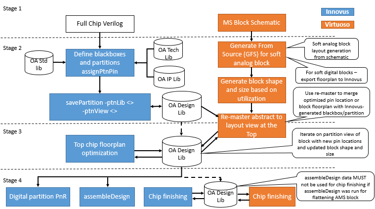
Floorplanning starts very early in the design cycle, sometimes even before a formal Verilog netlist is available. During stage one, a very early chip area estimate is done with determination of a rough floorplan, power resource allocation and IP locations. General routing resource allocation can also be obtained.
In stage two, chip designers can start populating the details of some of the blackboxes for which little or no information was available. During this stage, lot of iterations happen between top-level chip designer and the block implementation team where they negotiate between their implementation challenges.
In stage three, designers move more towards obtaining a much more mature chip. Analog mixed signal blocks might also become available during this stage. Some of the challenges of not having correct abstract are also identified and closed during this stage. Block or IP designers start delivering their final block databases.
In stage four, chip designers start their final sign-off checks. Keeping track of the ECO changes in the block and the top is a big challenge during this stage. Both the block and the top level implementation teams try to keep their blocks closed and clear all the sign-off checks.
Innovus and Virtuoso provide a rich set of commands and GUI functions to floorplan your design interactively. There are also commands for creating an initial floorplan automatically, or, resizing a finished floorplan while keeping relative placement of objects.
- For information on floorplan commands, see the Floorplan Commands chapter, in the Innovus Text Command Reference.
- For information on floorplan GUI, see the Floorplan Menu chapter, in the Innovus Menu Reference.
8.5.1 Floorplanning of Verilog Netlist Using Blackboxes
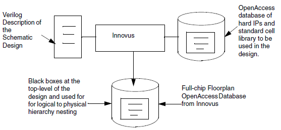
In Innovus, you can use the specifyBlackBox and definePartition commands to create early shapes for the hierarchical blocks where physical hierarchy has to be maintained. Follow with the partition and savePartition command sequence to save hierarchical black-boxes. You can run congestion and timing aware block and standard cell placement in Innovus.
You can use earlyGlobalRoute results for block pin optimization. Manual editing might be required for pin optimization to address grid, side-constraints, and alignment. Power planning, power routing and early power analysis is possible using sroute and Voltus in Innovus. The full-chip floorplan OpenAccess database is saved from Innovus. Use the savePartition -ptnLib <> -ptnView <> command to save hierarchical nested black boxes and partitions in the OpenAccess database.
8.5.1.1 Steps to Perform the Floorplanning of Verilog Netlist
- Set
setOaxMode -updateModetotrueto ensure complete interoperability. Create a configuration file within Innovus and use the top-chip Verilog netlist with OpenAccess reference libraries. Use the following variables while floorplanning a Verilog netlist: The following settings are for a design nameddtmf. The Verilog netlist name is dtmf_chip.v, and the top level cell name isdtmf_chip.set lefDefOutVersion {5.8}set init_abstract_view {abstract layout}set init_layout_view {layout}set init_pwr_net {vdd}set init_gnd_net {vss}set init_oa_ref_lib "techlib reflib"set init_verilog "dtmf_chip.v"
set init_design_netlisttype {Verilog}set init_top_cell {dtmf_chip}
Notes
- No LEF files are required. The library is read by Innovus using the OpenAccess technology and the standard cell library.
- The
init_abstract_view{abstract layout} variable uses the layout view to infer abstract information directly from the layout view using on-the-fly quick abstract inference utility within Innovus. This capability is used for fast-changing layout views of macros and this avoids the need of creating abstracts again.
From where is the tech information read?
If an OpenAccess design is read, the tech graph is analyzed from the design_lib that contains the cellview.
If a Verilog netlist is read with OpenAccess reference libraries, then the first library in the OpenAccess ref lib list is used for the tech. This means that the order of the ref libs is important when a Verilog netlist is used.
-
Additionally, sites and vias can be read from other libraries even though they are mostly considered to be tech information.
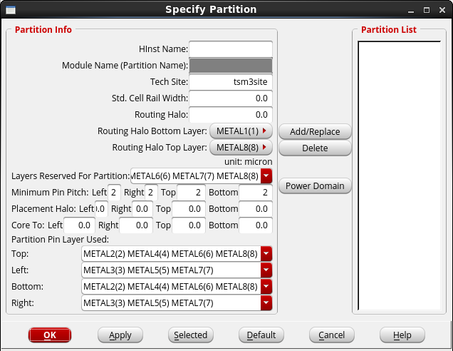
- After the design is imported in Innovus, use the Partition-Specify Black Box menu command to define a rectangular shape within the logical hierarchy.
Use Hierarchy Up/Down browser to reach to the logical hierarchy where you want to specify a black box. After the dark green box is obtained, you can make the box rectilinear according to your requirements and adjust it within the floorplan.
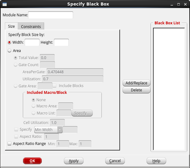
- Use the Partition-Specify Partition or Partition-Specify Black Box menu command to define a rectangular shape within the logical hierarchy which is required to have a separate physical hierarchy. This could be a soft analog block as well as a digital soft IP. You can use Hierarchy Up/Down browser to reach to the logical hierarchy which you want to specify as a partition. After the orange box is obtained, you can make the box rectilinear according to the requirement and fit it into the floorplan.
- Use the standard cell and block placer in Innovus to run timing-driven detailed placement of hard blocks and standard cells. You can use the
place_designcommand with its default setting (you can change the default by using thesetPlaceModecmd) to obtain automatic timing-driven and congestion-driven placement.
Innovus provides thesetPlaceModecmd to control the local cell density, local utilization, in-place optimization, timing targets, and so on, to control and guide the placement optimizer. Iterate this step to get optimal placement of partitions and blackboxes specified in the design. - After completing detailed placement, you can use
earlyGlobalRouteto get a quick estimate of the routing required. UsingearlyGlobalRoutealso helps in black box and partition pin assignment and pin layer and placement optimization. - Use the
savePartition-ptnLiblib_name-ptnViewlayout_view_namecommand in the Innovus command prompt to save the partitions in OpenAccess database. This will create a new library if the library name specified is not an existing name in thelib.deflist. Two new views are created for each partition and black boxes. The view name specified is used for creating the layout view that should be used for detailed physical implementation of the block. The other view that is created islayout_view_name_abstract, which is used as an abstract view of the block or partition or blackbox.
Whenever block shape, size or pin position or pin layer is changed, you should update this_abstractview because at the top level, the abstract view is referenced and used for detailed implementation. ThesavePartition-ptnLiblib_name-ptnViewlayout_view_namecommand will also create a new top level view by the namelayout_view_nameprovided as input. This top level view should be used for top-level implementation of the chip.
Note: Innovus allows blackboxes with a non-R0orientation to exist in the OpenAccess database. While reading a cellview that has a black box with non-R0orientation within Innovus, Innovus creates a geometric equivalent as theR0image of the blackbox within its virtual memory. While saving the design in the on-disk persistent OpenAccess database, Innovus will revert the black box instance to its original orientation.
Do not change the black box orientation during the Innovus session.
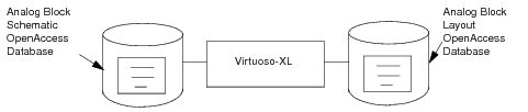
8.5.2 Generate From Source for Soft Analog Block Layout Using Virtuoso
This part of the flow takes place in the Virtuoso environment. In this step, the analog/mixed-signal block in the design will start to get implemented based on the schematic that has been captured for this part of the block.
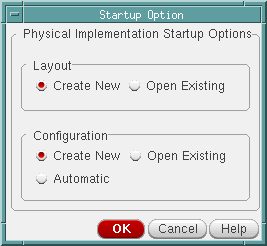
- Run Virtuoso Layout-GXL/XL from the schematic window. The following GUI is displayed:
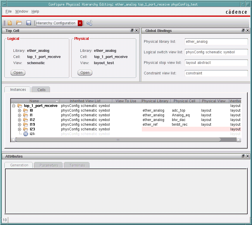
Configure Physical Hierarchy (CPH) is a shared interface between VLS-XL and Floorplanner available in Virtuoso. You can launch Virtuoso Layout-XL to generate layout view from the given schematic view. This layout view generated for the given schematic uses CPH information to process the generation of layout information according to the given constraints.
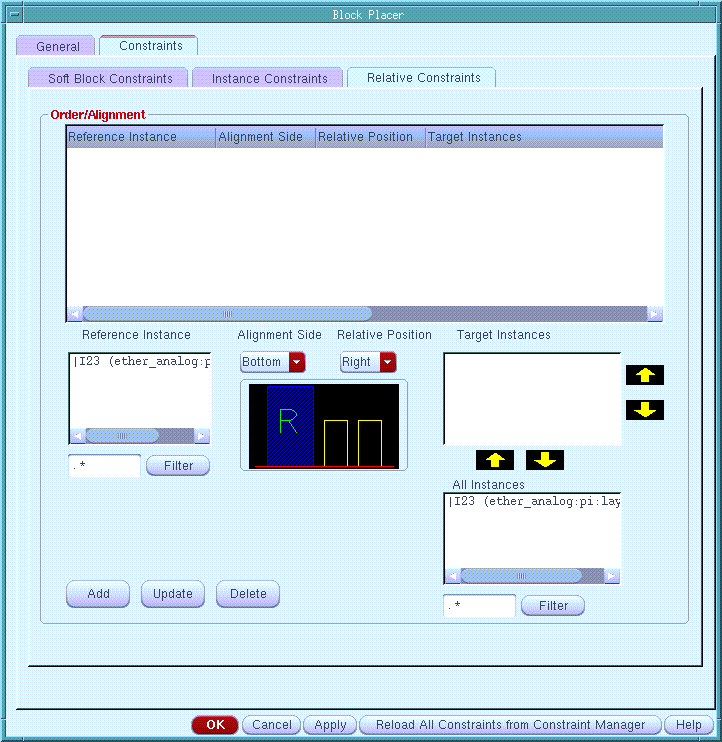
- The soft analog block boundary is automatically generated and you can reshape it to match the design constraints. You can run Virtuoso Block Placer to place bigger blocks inside the analog design module. The feature of Block Placer and menu details are shown in the figure below.
- The layout generation of a given design is an iterative process. As soon as first cut layout view is ready, save the layout view in OpenAccess database.
For more information, see Virtuoso Layout-XL User Guide.
8.5.3 Load Physical View to Merge Optimized Pin Locations and Block Boundary
This step of the flow also takes place in the Virtuoso environment. The Load Physical View command in Virtuoso is used to merge the optimized pin location done in Virtuoso with the floorplan created in Innovus for this block.
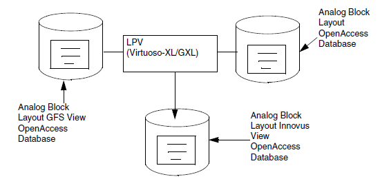
- Open the layout view of the soft analog block generated during the floorplanning of Verilog netlist and then call Load Physical View (LPV) to merge the optimized pin locations, layer information, size and updated block boundary generated during Generate from Source. The LPV form is available in the Virtuoso Layout-XL/GXL window. In the Choose Source Physical View field, enter the view name generated during Generate From Source.
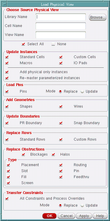
- If Virtuoso driven Analog block is completed 50 percent or greater, then merge using the following steps:
- Open analog block in Virtuoso.
- Set the status of critical pins to fixed.
- Do Load Physical View from the Innovus -generated soft block view.
- Create abstract to update the abstract view.
- Open Innovus generated soft block abstract.
- Set the status of critical pins to fixed (if needed).
- Load the physical view from the Virtuoso analog block.
- Create abstract to update the abstract view for top level usage.
- Update the abstract view of the soft analog block to avoid Innovus to read the full detailed layout view of the block.
8.5.4 Physical Implementation of Soft Analog Blocks Using Virtuoso
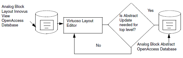
Since physical implementation of soft analog block is an iterative process, you can continue with further refinement of the analog block using Virtuoso Layout Editor. Keep the abstract view updated so that the top-level implementation place-and-route tool can get updated information about the analog blocks.
8.5.5 Physical Implementation of Soft Digital Blocks Using Innovus
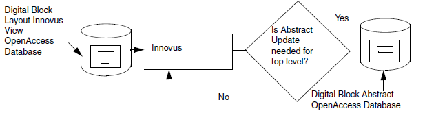
Physical Implementation of soft digital IPs/blocks can continue in parallel with detailed standard cells and hard blocks within the soft digital block placement, pre-CTS timing closure, CTS, post-CTS timing closure, clock net routing, detailed signal routing, SI and voltage analysis, and so on. This is an iterative process and might take long time. The final delivery after this step is the DRC and LVS clean layout view with all sign-off checks completed.
If the top-level STA flow requires block SPEFs, then run extraction and save the parasitic data back into OpenAccess. Keep the abstract view of the soft digital block updated and in-sync with the layout view to avoid any kind of layout mismatches at the top level-layout integration. The abstract view is required for the top-level integration because reading the detailed layout view and using that for place-and-route of the top level results in more run time. So, to avoid long run times, use the abstract view with boundary pins and metal blockages of the block.
8.6 Top-level Analog Net and Power Routing
At this point, you will use the top-level view saved from Innovus by using the savePartition command which will have the abstract view referenced for the partitions and blackboxes at the top level of the design. To do this, follow these guidelines:
- Perform analog net routing. Mark the nets as analog so that applications like Innovus can understand such instances/nets as analog and avoid optimization of such nets and instances. To route these nets, use the Virtuoso Space-Based Router (VSR).
- You can perform power net routing as required by the design in Innovus. The
sroutepower router can be used for detailed power routing and follow-pin connections to the top-level power grid. - VSR, a specialty available in Virtuoso platform, can be used for top-level analog net routing for 45nm and below technologies. It can also be called from within Innovus using the
run_vsrcommand. - With mixed signal routing constraints (DiffPair, MatchLength, NetClass and Shielding) interoperability possible, users are recommended to specify the IP and top-level routing constraints using recommended methods in either Virtuoso or Innovus platform. These constraints will be used throughout the implementation flow. For more information, refer to the Routing Constraint Interoperability chapter.
- PVS-CV tool can be used to validate the compliance of these constraints by net geometries. The tool can validate if the routing has been done manually or by automatic routers.
- The top-level critical and analog net routing can be done and pushed down as blockages into the partitions and blocks using the Virtuoso platform. Power nets can also be pushed inside the blocks for the blocks to use it for closing the connection with internal power network of the block.
Similarly, power planning and power routing can be done in Innovus before running thepartitioncommand and then the-pushDownSpecialNetAsObsoption can be used to push power routing and any signal routing or metal blockage as blockages inside the partitions created by Innovus.
Nanoroute, a digital router, should not be used for connecting the partially routed nets manually. If the partially routed sections of the net are left in the design and Nanoroute is run in either ECO or complete mode, multiple hanging routed segments are deleted by Nanoroute. To keep such partially manually routed sections of the signal routes, mark such nets as fixed. - The
saveDesign-cellviewcommand should be used withsetOaxMode-updateMode trueat the start of the session in Innovus to save design data in OpenAccess database. ThesetOaxModecommand should also be used at the start of the Innovus session. You cannot change the update mode settings in the middle of the session.
While saving from Virtuoso, do not change the top cell name used in Verilog netlist. Innovus always refers to the logical top cell name of the module used in the Verilog netlist for reading and writing the physical database.
8.7 Top-level Design Implementation
This portion of the flow is same as the digital foundation flow with all the mixed signal and analog blocks defined as blackboxes.
8.8 Final Chip Integration and Sign-Off
In this step:
- The
assembleDesigncommand in Innovus has been enhanced to run multi-level assembly within one single command. This automation can be used to assemble final routed database of the AMS blocks for performing more accurate timing and SI analysis.
- Transition time violations can be checked on long top level nets by STA engine and automatic buffers can be inserted on the violating nets within Innovus.
- Timing and SI ECOs can be performed by doing the changes in the final verilog netlist. ECOs done using the
ecoOaDesigncommand would retain the physical database sanctity during late stages of the design flow as well.
For more details, see the "Restoring the AMS Block Layout" section in the Static Timing Analysis for Mixed Signal Designs chapter.
8.9 ECO Flows
The Cadence platform based mixed signal solution offers a concurrent mixed signal floorplanning solution, which allows for efficient, frequent and smooth exchange of data between the top level designer and those designing the lower level blocks. The solution is implemented on the OpenAccess database, and allows for the exchange of floorplanning, placement and routing constraints. In addition, the environment offers the capability to embed mixed signal IP blocks with constraints that are used when instantiating such IPs within a design.
To address the challenges of performing ECOs on mixed signal designs, Cadence has implemented powerful ECO functionalities that perform ECOs on the actual OpenAccess database, containing both custom and place-and-route objects. For example, a design containing pcells can be ECO'ed in the Innovus environment without the need to separate out the custom objects in the design.
For information on pre- and post-mask ECO flows in Innovus on OpenAccess, refer to the "Innovus-Based ECO Flow" section in the Chip Finishing and ECO Flows chapter.